- Page 1 and 2:
Advanced Configuration and Power In
- Page 3 and 4:
Revision History Revision Change De
- Page 5 and 6:
Revision Change Description Affecte
- Page 7 and 8:
Revision Change Description Affecte
- Page 9 and 10:
Revision Change Description Affecte
- Page 11 and 12:
Revision Change Description Affecte
- Page 13 and 14:
Revision Change Description Affecte
- Page 15 and 16:
Contents 1 2 Introduction........
- Page 17 and 18:
5 ACPI Software Programming Model
- Page 19 and 20:
7 6.3.6 _RMV (Remove) ............
- Page 21 and 22:
9.2.5 _ALR (Ambient Light Response)
- Page 23 and 24:
11.2.1 Evaluating Thermal Device Li
- Page 25 and 26:
14.1.3 Generic Communications Subsp
- Page 27 and 28:
19.6.10 Buffer (Declare Buffer Obje
- Page 29 and 30:
19.6.102 Processor (Declare Process
- Page 31 and 32:
A.4.1 Power State Definitions......
- Page 33 and 34:
Tables Table 1-1 Hardware Type vs.
- Page 35 and 36:
Table 5-91 Power state Values .....
- Page 37 and 38:
Table 6-184 Device Insertion, Remov
- Page 39 and 40:
Table 10-275 Control Method Battery
- Page 41 and 42:
Table 19-367 Field Unit list entire
- Page 43 and 44:
Figures Figure 1-1 OSPM/ACPI Global
- Page 45 and 46:
Introduction 1 Introduction The Adv
- Page 47 and 48:
Introduction wake and answer the te
- Page 49 and 50:
Introduction Figure 1-1 OSPM/ACPI G
- Page 51 and 52:
Introduction specified below are ge
- Page 53 and 54:
Introduction ACPI System Descriptio
- Page 55 and 56:
Introduction • Support the ACPI E
- Page 57 and 58:
Introduction 1.9.2 Programming Mode
- Page 59 and 60:
Introduction 1.10 Related Documents
- Page 61 and 62:
Definition of Terms 2 Definition of
- Page 63 and 64:
Definition of Terms of power manage
- Page 65 and 66:
Definition of Terms I/O SAPIC An In
- Page 67 and 68:
Definition of Terms loaded. This al
- Page 69 and 70:
Definition of Terms varies on the w
- Page 71 and 72:
Definition of Terms in shallower po
- Page 73 and 74:
Definition of Terms state to allow
- Page 75 and 76:
ACPI Overview 3 ACPI Overview Platf
- Page 77 and 78:
ACPI Overview component to avoid da
- Page 79 and 80:
ACPI Overview Aspects of mobile PC
- Page 81 and 82:
ACPI Overview level, platform-speci
- Page 83 and 84:
ACPI Overview through their own bus
- Page 85 and 86:
ACPI Overview the SCI status bit ma
- Page 87 and 88:
ACPI Overview wait for the call. To
- Page 89 and 90:
ACPI Overview Each device enumerate
- Page 91 and 92:
ACPI Overview the battery is able t
- Page 93 and 94:
ACPI Overview Table 3-4 Level Warni
- Page 95 and 96:
ACPI Overview necessary. Figure 3-8
- Page 97 and 98:
ACPI Overview 3.11.1 Hardware-reduc
- Page 99 and 100:
ACPI Overview Low Power S0 Idle Cap
- Page 101 and 102:
ACPI Hardware Specification 4 ACPI
- Page 103 and 104:
ACPI Hardware Specification would b
- Page 105 and 106:
ACPI Hardware Specification OSPM re
- Page 107 and 108:
ACPI Hardware Specification SLP_ENx
- Page 109 and 110:
ACPI Hardware Specification Device
- Page 111 and 112:
ACPI Hardware Specification Generic
- Page 113 and 114:
ACPI Hardware Specification Feature
- Page 115 and 116:
ACPI Hardware Specification Registe
- Page 117 and 118:
ACPI Hardware Specification Table 4
- Page 119 and 120:
ACPI Hardware Specification purpose
- Page 121 and 122:
ACPI Hardware Specification The pow
- Page 123 and 124:
ACPI Hardware Specification 4.8.2.2
- Page 125 and 126:
ACPI Hardware Specification 4.8.2.3
- Page 127 and 128:
ACPI Hardware Specification Month A
- Page 129 and 130:
ACPI Hardware Specification • OSP
- Page 131 and 132:
ACPI Hardware Specification Bit Nam
- Page 133 and 134:
ACPI Hardware Specification Althoug
- Page 135 and 136:
ACPI Hardware Specification 4.8.3.5
- Page 137 and 138:
ACPI Hardware Specification the SLE
- Page 139 and 140:
ACPI Hardware Specification Power B
- Page 141 and 142:
ACPI Hardware Specification ACPI FA
- Page 143 and 144:
ACPI Hardware Specification This lo
- Page 145 and 146:
ACPI Software Programming Model 5 A
- Page 147 and 148:
ACPI Software Programming Model The
- Page 149 and 150:
ACPI Software Programming Model •
- Page 151 and 152:
ACPI Software Programming Model The
- Page 153 and 154:
ACPI Software Programming Model ACP
- Page 155 and 156:
ACPI Software Programming Model OEM
- Page 157 and 158:
ACPI Software Programming Model Sig
- Page 159 and 160:
ACPI Software Programming Model 5.2
- Page 161 and 162:
ACPI Software Programming Model Fie
- Page 163 and 164:
ACPI Software Programming Model Fie
- Page 165 and 166:
ACPI Software Programming Model Fie
- Page 167 and 168:
ACPI Software Programming Model Fie
- Page 169 and 170:
ACPI Software Programming Model FAC
- Page 171 and 172:
ACPI Software Programming Model FAC
- Page 173 and 174: ACPI Software Programming Model tha
- Page 175 and 176: ACPI Software Programming Model Fie
- Page 177 and 178: ACPI Software Programming Model Tab
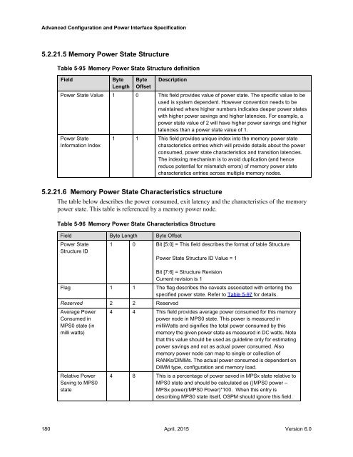
- Page 179 and 180: ACPI Software Programming Model Rel
- Page 181 and 182: ACPI Software Programming Model Fie
- Page 183 and 184: ACPI Software Programming Model Fie
- Page 185 and 186: ACPI Software Programming Model Ena
- Page 187 and 188: ACPI Software Programming Model Int
- Page 189 and 190: ACPI Software Programming Model as
- Page 191 and 192: ACPI Software Programming Model Tab
- Page 193 and 194: ACPI Software Programming Model Glo
- Page 195 and 196: ACPI Software Programming Model Fie
- Page 197 and 198: ACPI Software Programming Model Fie
- Page 199 and 200: ACPI Software Programming Model Glo
- Page 201 and 202: ACPI Software Programming Model Fie
- Page 203 and 204: ACPI Software Programming Model OEM
- Page 205 and 206: ACPI Software Programming Model Res
- Page 207 and 208: ACPI Software Programming Model Fie
- Page 209 and 210: ACPI Software Programming Model Tab
- Page 211 and 212: ACPI Software Programming Model RAS
- Page 213 and 214: ACPI Software Programming Model 2-1
- Page 215 and 216: ACPI Software Programming Model Sec
- Page 217 and 218: ACPI Software Programming Model Tab
- Page 219 and 220: ACPI Software Programming Model MEM
- Page 221 and 222: ACPI Software Programming Model Tab
- Page 223: ACPI Software Programming Model Fie
- Page 227 and 228: ACPI Software Programming Model Sco
- Page 229 and 230: ACPI Software Programming Model Fla
- Page 231 and 232: ACPI Software Programming Model Fie
- Page 233 and 234: ACPI Software Programming Model 5.2
- Page 235 and 236: ACPI Software Programming Model Fie
- Page 237 and 238: ACPI Software Programming Model the
- Page 239 and 240: ACPI Software Programming Model 5.2
- Page 241 and 242: ACPI Software Programming Model Fie
- Page 243 and 244: ACPI Software Programming Model Fie
- Page 245 and 246: ACPI Software Programming Model Tab
- Page 247 and 248: ACPI Software Programming Model NFI
- Page 249 and 250: ACPI Software Programming Model The
- Page 251 and 252: ACPI Software Programming Model Fie
- Page 253 and 254: ACPI Software Programming Model Typ
- Page 255 and 256: ACPI Software Programming Model Sof
- Page 257 and 258: ACPI Software Programming Model •
- Page 259 and 260: ACPI Software Programming Model Nam
- Page 261 and 262: ACPI Software Programming Model (1)
- Page 263 and 264: ACPI Software Programming Model 5.5
- Page 265 and 266: ACPI Software Programming Model acc
- Page 267 and 268: ACPI Software Programming Model 5.5
- Page 269 and 270: ACPI Software Programming Model IPM
- Page 271 and 272: ACPI Software Programming Model Not
- Page 273 and 274: ACPI Software Programming Model Ope
- Page 275 and 276:
ACPI Software Programming Model •
- Page 277 and 278:
ACPI Software Programming Model /*
- Page 279 and 280:
ACPI Software Programming Model //
- Page 281 and 282:
ACPI Software Programming Model //
- Page 283 and 284:
ACPI Software Programming Model The
- Page 285 and 286:
ACPI Software Programming Model //
- Page 287 and 288:
ACPI Software Programming Model 5.6
- Page 289 and 290:
ACPI Software Programming Model eve
- Page 291 and 292:
ACPI Software Programming Model •
- Page 293 and 294:
ACPI Software Programming Model 5.6
- Page 295 and 296:
ACPI Software Programming Model Val
- Page 297 and 298:
ACPI Software Programming Model Tab
- Page 299 and 300:
ACPI Software Programming Model Tab
- Page 301 and 302:
ACPI Software Programming Model Plu
- Page 303 and 304:
ACPI Software Programming Model Nam
- Page 305 and 306:
ACPI Software Programming Model Nam
- Page 307 and 308:
ACPI Software Programming Model Nam
- Page 309 and 310:
ACPI Software Programming Model Nam
- Page 311 and 312:
ACPI Software Programming Model Nam
- Page 313 and 314:
ACPI Software Programming Model Nam
- Page 315 and 316:
ACPI Software Programming Model Fea
- Page 317 and 318:
ACPI Software Programming Model Def
- Page 319 and 320:
ACPI Software Programming Model Exa
- Page 321 and 322:
Device Configuration 6 Device Confi
- Page 323 and 324:
Device Configuration BUS PCMCIA PC
- Page 325 and 326:
Device Configuration Device(SATA) /
- Page 327 and 328:
Device Configuration Return Value I
- Page 329 and 330:
Device Configuration unable to dete
- Page 331 and 332:
Device Configuration Name Definitio
- Page 333 and 334:
Device Configuration Name Definitio
- Page 335 and 336:
Device Configuration Rota-tion Goup
- Page 337 and 338:
Device Configuration Example ASL: N
- Page 339 and 340:
Device Configuration Object _FIX _G
- Page 341 and 342:
Device Configuration For example, i
- Page 343 and 344:
Device Configuration 6.2.5 _DSD (De
- Page 345 and 346:
Device Configuration } Name (_DSD,
- Page 347 and 348:
Device Configuration APIC Device”
- Page 349 and 350:
Device Configuration Scope(\_SB) {
- Page 351 and 352:
Device Configuration Method(_EJ0, 1
- Page 353 and 354:
Device Configuration Field Object T
- Page 355 and 356:
Device Configuration Field Object T
- Page 357 and 358:
Device Configuration other governin
- Page 359 and 360:
Device Configuration Since platform
- Page 361 and 362:
Device Configuration Section 8.4.4.
- Page 363 and 364:
Device Configuration Control Field
- Page 365 and 366:
Device Configuration Device(PCI0) /
- Page 367 and 368:
Device Configuration Field Type Des
- Page 369 and 370:
Device Configuration This optional
- Page 371 and 372:
Device Configuration Field Byte Len
- Page 373 and 374:
Device Configuration If a device in
- Page 375 and 376:
Device Configuration are present, w
- Page 377 and 378:
Device Configuration Arguments: Non
- Page 379 and 380:
Device Configuration Return Value:
- Page 381 and 382:
Device Configuration Table 6-187 Op
- Page 383 and 384:
Device Configuration User interacts
- Page 385 and 386:
Device Configuration Method(_EJ0, 1
- Page 387 and 388:
Device Configuration 6.4.2 Small Re
- Page 389 and 390:
Device Configuration Offset Field N
- Page 391 and 392:
Device Configuration Table 6-197 I/
- Page 393 and 394:
Device Configuration 6.4.2.9 End Ta
- Page 395 and 396:
Device Configuration Offset Byte 11
- Page 397 and 398:
Device Configuration Offset Field N
- Page 399 and 400:
Device Configuration Offset Field N
- Page 401 and 402:
Device Configuration Offset Field N
- Page 403 and 404:
Device Configuration Offset Field N
- Page 405 and 406:
Device Configuration Offset Field N
- Page 407 and 408:
Device Configuration Offset Field N
- Page 409 and 410:
Device Configuration Offset Field N
- Page 411 and 412:
Device Configuration To specify mul
- Page 413 and 414:
Device Configuration Offset Field N
- Page 415 and 416:
Device Configuration Offset Field N
- Page 417 and 418:
Device Configuration Offset Field N
- Page 419 and 420:
Device Configuration Offset Field N
- Page 421 and 422:
Device Configuration Offset Field N
- Page 423 and 424:
Device Configuration Offset Field N
- Page 425 and 426:
Device Configuration 6.5 Other Obje
- Page 427 and 428:
Device Configuration Note: If the m
- Page 429 and 430:
Device Configuration Note: The OS o
- Page 431 and 432:
Device Configuration whether the Gl
- Page 433 and 434:
Power and Performance Management 7
- Page 435 and 436:
Power and Performance Management No
- Page 437 and 438:
Power and Performance Management Re
- Page 439 and 440:
Power and Performance Management Ob
- Page 441 and 442:
Power and Performance Management Ar
- Page 443 and 444:
Power and Performance Management Re
- Page 445 and 446:
Power and Performance Management Re
- Page 447 and 448:
Power and Performance Management Ar
- Page 449 and 450:
Power and Performance Management If
- Page 451 and 452:
Power and Performance Management Re
- Page 453 and 454:
Power and Performance Management Ar
- Page 455 and 456:
Power and Performance Management ca
- Page 457 and 458:
Power and Performance Management
- Page 459 and 460:
Power and Performance Management im
- Page 461 and 462:
Power and Performance Management 9.
- Page 463 and 464:
Processor Configuration and Control
- Page 465 and 466:
Processor Configuration and Control
- Page 467 and 468:
Processor Configuration and Control
- Page 469 and 470:
Processor Configuration and Control
- Page 471 and 472:
Processor Configuration and Control
- Page 473 and 474:
Processor Configuration and Control
- Page 475 and 476:
Processor Configuration and Control
- Page 477 and 478:
Processor Configuration and Control
- Page 479 and 480:
Processor Configuration and Control
- Page 481 and 482:
Processor Configuration and Control
- Page 483 and 484:
Processor Configuration and Control
- Page 485 and 486:
Processor Configuration and Control
- Page 487 and 488:
Processor Configuration and Control
- Page 489 and 490:
Processor Configuration and Control
- Page 491 and 492:
Processor Configuration and Control
- Page 493 and 494:
Processor Configuration and Control
- Page 495 and 496:
Processor Configuration and Control
- Page 497 and 498:
Processor Configuration and Control
- Page 499 and 500:
Processor Configuration and Control
- Page 501 and 502:
Processor Configuration and Control
- Page 503 and 504:
Processor Configuration and Control
- Page 505 and 506:
Processor Configuration and Control
- Page 507 and 508:
Processor Configuration and Control
- Page 509 and 510:
Processor Configuration and Control
- Page 511 and 512:
Processor Configuration and Control
- Page 513 and 514:
Processor Configuration and Control
- Page 515 and 516:
Processor Configuration and Control
- Page 517 and 518:
Processor Configuration and Control
- Page 519 and 520:
Processor Configuration and Control
- Page 521 and 522:
Processor Configuration and Control
- Page 523 and 524:
Processor Configuration and Control
- Page 525 and 526:
Processor Configuration and Control
- Page 527 and 528:
Processor Configuration and Control
- Page 529 and 530:
Processor Configuration and Control
- Page 531 and 532:
Processor Configuration and Control
- Page 533 and 534:
Processor Configuration and Control
- Page 535 and 536:
Processor Configuration and Control
- Page 537 and 538:
Processor Configuration and Control
- Page 539 and 540:
Processor Configuration and Control
- Page 541 and 542:
ACPI-Defined Devices and Device-Spe
- Page 543 and 544:
ACPI-Defined Devices and Device-Spe
- Page 545 and 546:
ACPI-Defined Devices and Device-Spe
- Page 547 and 548:
ACPI-Defined Devices and Device-Spe
- Page 549 and 550:
ACPI-Defined Devices and Device-Spe
- Page 551 and 552:
ACPI-Defined Devices and Device-Spe
- Page 553 and 554:
ACPI-Defined Devices and Device-Spe
- Page 555 and 556:
ACPI-Defined Devices and Device-Spe
- Page 557 and 558:
ACPI-Defined Devices and Device-Spe
- Page 559 and 560:
ACPI-Defined Devices and Device-Spe
- Page 561 and 562:
ACPI-Defined Devices and Device-Spe
- Page 563 and 564:
ACPI-Defined Devices and Device-Spe
- Page 565 and 566:
ACPI-Defined Devices and Device-Spe
- Page 567 and 568:
ACPI-Defined Devices and Device-Spe
- Page 569 and 570:
ACPI-Defined Devices and Device-Spe
- Page 571 and 572:
ACPI-Defined Devices and Device-Spe
- Page 573 and 574:
ACPI-Defined Devices and Device-Spe
- Page 575 and 576:
ACPI-Defined Devices and Device-Spe
- Page 577 and 578:
ACPI-Defined Devices and Device-Spe
- Page 579 and 580:
ACPI-Defined Devices and Device-Spe
- Page 581 and 582:
ACPI-Defined Devices and Device-Spe
- Page 583 and 584:
ACPI-Defined Devices and Device-Spe
- Page 585 and 586:
ACPI-Defined Devices and Device-Spe
- Page 587 and 588:
ACPI-Defined Devices and Device-Spe
- Page 589 and 590:
ACPI-Defined Devices and Device-Spe
- Page 591 and 592:
ACPI-Defined Devices and Device-Spe
- Page 593 and 594:
ACPI-Defined Devices and Device-Spe
- Page 595 and 596:
ACPI-Defined Devices and Device-Spe
- Page 597 and 598:
ACPI-Defined Devices and Device-Spe
- Page 599 and 600:
ACPI-Defined Devices and Device-Spe
- Page 601 and 602:
ACPI-Defined Devices and Device-Spe
- Page 603 and 604:
ACPI-Defined Devices and Device-Spe
- Page 605 and 606:
Power Source and Power Meter Device
- Page 607 and 608:
Power Source and Power Meter Device
- Page 609 and 610:
Power Source and Power Meter Device
- Page 611 and 612:
Power Source and Power Meter Device
- Page 613 and 614:
Power Source and Power Meter Device
- Page 615 and 616:
Power Source and Power Meter Device
- Page 617 and 618:
Power Source and Power Meter Device
- Page 619 and 620:
Power Source and Power Meter Device
- Page 621 and 622:
Power Source and Power Meter Device
- Page 623 and 624:
Power Source and Power Meter Device
- Page 625 and 626:
Power Source and Power Meter Device
- Page 627 and 628:
Power Source and Power Meter Device
- Page 629 and 630:
Power Source and Power Meter Device
- Page 631 and 632:
Power Source and Power Meter Device
- Page 633 and 634:
Power Source and Power Meter Device
- Page 635 and 636:
Power Source and Power Meter Device
- Page 637 and 638:
Thermal Management 11 Thermal Manag
- Page 639 and 640:
Thermal Management When a thermal z
- Page 641 and 642:
Thermal Management controller firmw
- Page 643 and 644:
Thermal Management 11.1.5 Passive C
- Page 645 and 646:
Thermal Management 11.2 Cooling Pre
- Page 647 and 648:
Thermal Management Alternatively, d
- Page 649 and 650:
Thermal Management 11.3.1.2 _FPS (F
- Page 651 and 652:
Thermal Management Package (){ Revi
- Page 653 and 654:
Thermal Management 11.4.2 _ALx (Act
- Page 655 and 656:
Thermal Management Element Object T
- Page 657 and 658:
Thermal Management Return Value: No
- Page 659 and 660:
Thermal Management Other Temperatur
- Page 661 and 662:
Thermal Management // // NOTE3: Thi
- Page 663 and 664:
Thermal Management 11.4.16 _TFP (Th
- Page 665 and 666:
Thermal Management 11.4.20 _TSN (Th
- Page 667 and 668:
Thermal Management occurs—relievi
- Page 669 and 670:
Thermal Management Scope(\_SB) { De
- Page 671 and 672:
Thermal Management } // fan cooling
- Page 673 and 674:
Thermal Management // For brevity,
- Page 675 and 676:
Thermal Management External(\_SB.CP
- Page 677 and 678:
Thermal Management Method(_TPT, 1)
- Page 679 and 680:
ACPI Embedded Controller Interface
- Page 681 and 682:
ACPI Embedded Controller Interface
- Page 683 and 684:
ACPI Embedded Controller Interface
- Page 685 and 686:
ACPI Embedded Controller Interface
- Page 687 and 688:
ACPI Embedded Controller Interface
- Page 689 and 690:
ACPI Embedded Controller Interface
- Page 691 and 692:
ACPI Embedded Controller Interface
- Page 693 and 694:
ACPI Embedded Controller Interface
- Page 695 and 696:
ACPI Embedded Controller Interface
- Page 697 and 698:
ACPI Embedded Controller Interface
- Page 699 and 700:
ACPI Embedded Controller Interface
- Page 701 and 702:
ACPI Embedded Controller Interface
- Page 703 and 704:
ACPI Embedded Controller Interface
- Page 705 and 706:
ACPI System Management Bus Interfac
- Page 707 and 708:
ACPI System Management Bus Interfac
- Page 709 and 710:
ACPI System Management Bus Interfac
- Page 711 and 712:
ACPI System Management Bus Interfac
- Page 713 and 714:
ACPI System Management Bus Interfac
- Page 715 and 716:
ACPI System Management Bus Interfac
- Page 717 and 718:
ACPI System Management Bus Interfac
- Page 719 and 720:
Platform Communications Channel (PC
- Page 721 and 722:
Platform Communications Channel (PC
- Page 723 and 724:
Platform Communications Channel (PC
- Page 725 and 726:
Platform Communications Channel (PC
- Page 727 and 728:
System Address Map Interfaces 15 Sy
- Page 729 and 730:
System Address Map Interfaces EAX F
- Page 731 and 732:
System Address Map Interfaces 15.3
- Page 733 and 734:
System Address Map Interfaces Base
- Page 735 and 736:
Waking and Sleeping 16 Waking and S
- Page 737 and 738:
Waking and Sleeping 16.1 Sleeping S
- Page 739 and 740:
Waking and Sleeping synchronized wi
- Page 741 and 742:
Waking and Sleeping 3. Removing pow
- Page 743 and 744:
Waking and Sleeping The _TTS contro
- Page 745 and 746:
Waking and Sleeping on what the har
- Page 747 and 748:
Waking and Sleeping CLI instruction
- Page 749 and 750:
Waking and Sleeping For this exampl
- Page 751 and 752:
Waking and Sleeping If an NVS image
- Page 753 and 754:
Platforms Non-Uniform Memory Access
- Page 755 and 756:
Platforms Non-Uniform Memory Access
- Page 757 and 758:
ACPI Platform Error Interfaces (APE
- Page 759 and 760:
ACPI Platform Error Interfaces (APE
- Page 761 and 762:
ACPI Platform Error Interfaces (APE
- Page 763 and 764:
ACPI Platform Error Interfaces (APE
- Page 765 and 766:
ACPI Platform Error Interfaces (APE
- Page 767 and 768:
ACPI Platform Error Interfaces (APE
- Page 769 and 770:
ACPI Platform Error Interfaces (APE
- Page 771 and 772:
ACPI Platform Error Interfaces (APE
- Page 773 and 774:
ACPI Platform Error Interfaces (APE
- Page 775 and 776:
ACPI Platform Error Interfaces (APE
- Page 777 and 778:
ACPI Platform Error Interfaces (APE
- Page 779 and 780:
ACPI Platform Error Interfaces (APE
- Page 781 and 782:
ACPI Platform Error Interfaces (APE
- Page 783 and 784:
ACPI Platform Error Interfaces (APE
- Page 785 and 786:
ACPI Platform Error Interfaces (APE
- Page 787 and 788:
ACPI Platform Error Interfaces (APE
- Page 789 and 790:
ACPI Platform Error Interfaces (APE
- Page 791 and 792:
ACPI Platform Error Interfaces (APE
- Page 793 and 794:
ACPI Platform Error Interfaces (APE
- Page 795 and 796:
ACPI Source Language (ASL)Reference
- Page 797 and 798:
ACPI Source Language (ASL)Reference
- Page 799 and 800:
ACPI Source Language (ASL)Reference
- Page 801 and 802:
ACPI Source Language (ASL)Reference
- Page 803 and 804:
ACPI Source Language (ASL)Reference
- Page 805 and 806:
ACPI Source Language (ASL)Reference
- Page 807 and 808:
ACPI Source Language (ASL)Reference
- Page 809 and 810:
ACPI Source Language (ASL)Reference
- Page 811 and 812:
ACPI Source Language (ASL)Reference
- Page 813 and 814:
ACPI Source Language (ASL)Reference
- Page 815 and 816:
ACPI Source Language (ASL)Reference
- Page 817 and 818:
ACPI Source Language (ASL)Reference
- Page 819 and 820:
ACPI Source Language (ASL)Reference
- Page 821 and 822:
ACPI Source Language (ASL)Reference
- Page 823 and 824:
ACPI Source Language (ASL)Reference
- Page 825 and 826:
ACPI Source Language (ASL)Reference
- Page 827 and 828:
ACPI Source Language (ASL)Reference
- Page 829 and 830:
ACPI Source Language (ASL)Reference
- Page 831 and 832:
ACPI Source Language (ASL)Reference
- Page 833 and 834:
ACPI Source Language (ASL)Reference
- Page 835 and 836:
ACPI Source Language (ASL)Reference
- Page 837 and 838:
ACPI Source Language (ASL)Reference
- Page 839 and 840:
ACPI Source Language (ASL)Reference
- Page 841 and 842:
ACPI Source Language (ASL)Reference
- Page 843 and 844:
ACPI Source Language (ASL)Reference
- Page 845 and 846:
ACPI Source Language (ASL)Reference
- Page 847 and 848:
ACPI Source Language (ASL)Reference
- Page 849 and 850:
ACPI Source Language (ASL)Reference
- Page 851 and 852:
ACPI Source Language (ASL)Reference
- Page 853 and 854:
ACPI Source Language (ASL)Reference
- Page 855 and 856:
ACPI Source Language (ASL)Reference
- Page 857 and 858:
ACPI Source Language (ASL)Reference
- Page 859 and 860:
ACPI Source Language (ASL)Reference
- Page 861 and 862:
ACPI Source Language (ASL)Reference
- Page 863 and 864:
ACPI Source Language (ASL)Reference
- Page 865 and 866:
ACPI Source Language (ASL)Reference
- Page 867 and 868:
ACPI Source Language (ASL)Reference
- Page 869 and 870:
ACPI Source Language (ASL)Reference
- Page 871 and 872:
ACPI Source Language (ASL)Reference
- Page 873 and 874:
ACPI Source Language (ASL)Reference
- Page 875 and 876:
ACPI Source Language (ASL)Reference
- Page 877 and 878:
ACPI Source Language (ASL)Reference
- Page 879 and 880:
ACPI Source Language (ASL)Reference
- Page 881 and 882:
ACPI Source Language (ASL)Reference
- Page 883 and 884:
ACPI Source Language (ASL)Reference
- Page 885 and 886:
ACPI Source Language (ASL)Reference
- Page 887 and 888:
ACPI Source Language (ASL)Reference
- Page 889 and 890:
ACPI Source Language (ASL)Reference
- Page 891 and 892:
ACPI Source Language (ASL)Reference
- Page 893 and 894:
ACPI Source Language (ASL)Reference
- Page 895 and 896:
ACPI Source Language (ASL)Reference
- Page 897 and 898:
ACPI Source Language (ASL)Reference
- Page 899 and 900:
ACPI Source Language (ASL)Reference
- Page 901 and 902:
ACPI Source Language (ASL)Reference
- Page 903 and 904:
ACPI Source Language (ASL)Reference
- Page 905 and 906:
ACPI Source Language (ASL)Reference
- Page 907 and 908:
ACPI Source Language (ASL)Reference
- Page 909 and 910:
ACPI Source Language (ASL)Reference
- Page 911 and 912:
ACPI Source Language (ASL)Reference
- Page 913 and 914:
ACPI Source Language (ASL)Reference
- Page 915 and 916:
ACPI Source Language (ASL)Reference
- Page 917 and 918:
ACPI Source Language (ASL)Reference
- Page 919 and 920:
ACPI Source Language (ASL)Reference
- Page 921 and 922:
ACPI Source Language (ASL)Reference
- Page 923 and 924:
ACPI Source Language (ASL)Reference
- Page 925 and 926:
ACPI Source Language (ASL)Reference
- Page 927 and 928:
ACPI Source Language (ASL)Reference
- Page 929 and 930:
ACPI Source Language (ASL)Reference
- Page 931 and 932:
ACPI Source Language (ASL)Reference
- Page 933 and 934:
ACPI Source Language (ASL)Reference
- Page 935 and 936:
ACPI Source Language (ASL)Reference
- Page 937 and 938:
ACPI Source Language (ASL)Reference
- Page 939 and 940:
ACPI Source Language (ASL)Reference
- Page 941 and 942:
ACPI Source Language (ASL)Reference
- Page 943 and 944:
ACPI Source Language (ASL)Reference
- Page 945 and 946:
ACPI Source Language (ASL)Reference
- Page 947 and 948:
ACPI Source Language (ASL)Reference
- Page 949 and 950:
ACPI Source Language (ASL)Reference
- Page 951 and 952:
ACPI Machine Language (AML) Specifi
- Page 953 and 954:
ACPI Machine Language (AML) Specifi
- Page 955 and 956:
ACPI Machine Language (AML) Specifi
- Page 957 and 958:
ACPI Machine Language (AML) Specifi
- Page 959 and 960:
ACPI Machine Language (AML) Specifi
- Page 961 and 962:
ACPI Machine Language (AML) Specifi
- Page 963 and 964:
ACPI Machine Language (AML) Specifi
- Page 965 and 966:
ACPI Machine Language (AML) Specifi
- Page 967 and 968:
ACPI Machine Language (AML) Specifi
- Page 969 and 970:
ACPI Machine Language (AML) Specifi
- Page 971 and 972:
ACPI Data Tables and Table Definiti
- Page 973 and 974:
ACPI Data Tables and Table Definiti
- Page 975 and 976:
ACPI Data Tables and Table Definiti
- Page 977 and 978:
ACPI Data Tables and Table Definiti
- Page 979 and 980:
ACPI Data Tables and Table Definiti
- Page 981 and 982:
ACPI Data Tables and Table Definiti
- Page 983 and 984:
ACPI Data Tables and Table Definiti
- Page 985 and 986:
Appendix A Device Class Specificati
- Page 987 and 988:
• PCI Bus Power Management Capabi
- Page 989 and 990:
A.4.1 Power State Definitions State
- Page 991 and 992:
A.5.1 Power State Definitions State
- Page 993 and 994:
A.6.1.2 Internal Flat Panel Devices
- Page 995 and 996:
power transitions and power managem
- Page 997 and 998:
A video controller conforming to th
- Page 999 and 1000:
State Status Definition D2 N/A This
- Page 1001 and 1002:
The most common modem type is an IS
- Page 1003 and 1004:
State Status Definition D1 Optional
- Page 1005 and 1006:
A.10.1 Power State Definitions Stat
- Page 1007 and 1008:
A.11.1 Power State Definitions A.11
- Page 1009 and 1010:
A floppy disk and IDE channel devic
- Page 1011 and 1012:
Appendix B Video Extensions B.1 ACP
- Page 1013 and 1014:
GPE // ACPI General-purpose HW even
- Page 1015 and 1016:
B.3.2 _DOD (Enumerate All Devices A
- Page 1017 and 1018:
Pipe / Head Ports Display Types Dis
- Page 1019 and 1020:
the next boot, a 1 indicates a PCI
- Page 1021 and 1022:
Value 0x84 Description Previous Dis
- Page 1023 and 1024:
B.5.5 _DDC (Return the EDID for thi
- Page 1025 and 1026:
Bits Definition 31 0 - Don’t do a
- Page 1027 and 1028:
internal data structure of the OS t
- Page 1029 and 1030:
Symbols _EJx 334 ??????????????????
- Page 1031 and 1032:
Power Resource statements 391 prima
- Page 1033 and 1034:
centenary value, RTC alarm 83 Centr
- Page 1035 and 1036:
power resource objects 398 D2 Devic
- Page 1037 and 1038:
Eject Device List (_EDL) object 332
- Page 1039 and 1040:
features 68 functional implementati
- Page 1041 and 1042:
I/O resource flag 366 I/O SAPIC def
- Page 1043 and 1044:
logic fixed power button 77 lid swi
- Page 1045 and 1046:
objects _ BMC (Battery Maintenance
- Page 1047 and 1048:
transitioning working to soft-off s
- Page 1049 and 1050:
power resources battery management
- Page 1051 and 1052:
definition 22 table fields 115 RTC_
- Page 1053 and 1054:
protocols 650, 662, 669 Read/Write
- Page 1055 and 1056:
top of memory 704 ToString (Convert