Association
Magnetic Oxide Heterostructures: EuO on Cubic Oxides ... - JuSER
Magnetic Oxide Heterostructures: EuO on Cubic Oxides ... - JuSER
- No tags were found...

Create successful ePaper yourself
Turn your PDF publications into a flip-book with our unique Google optimized e-Paper software.
3.4. Ex situ characterization techniques 53<br />
<br />
<br />
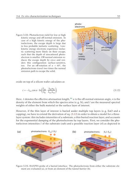
Figure 3.18.: Photoelectron yield for low or high<br />
kinetic energy and off-normal emission. In<br />
case of a high kinetic energy of the photoelectrons,<br />
the escape depth is large due<br />
to less probable inelastic scattering. Lowkinetic<br />
energy electrons experience inelastic<br />
scattering more likely on their escape,<br />
such that the depth of unscattered photoelectron<br />
is smaller. Off-normal emission reduces<br />
the escape depth by cosα and renders<br />
this configuration surface-sensitive,<br />
too. For an off-rotation of α =60 ◦ , the<br />
photoelectrons travel two times the normal<br />
emission path to escape the solid.<br />
<br />
<br />
<br />
<br />
<br />
<br />
<br />
<br />
<br />
<br />
<br />
oxide on top of a silicon wafer calculates as<br />
(<br />
Iox<br />
c = −λ ox cosα ·ln · λSin<br />
)<br />
Si<br />
. (3.12)<br />
I Si λ ox n ox<br />
Here, λ denotes the effective attenuation length, 84 α is the off-normal emission angle, n is the<br />
density of the element from which the spectra arise (e. g. Si), and I are the measured spectral<br />
weights of either the bulk material or the surface layer of interest.<br />
However, if the thin layer of interest is buried under multiple top layers (e. g. EuO and a<br />
capping), we have to extend the derivation of eq. (3.12) in order to obtain a model for a threelayer<br />
system: this includes intensities of a substrate, a thin buried reaction layer, and accounts<br />
for the exponential damping of the photoelectrons by top layers. First, we consider the photoelectron<br />
intensities I of the substrate (sub) and a possible reaction layer (rl) as depicted in<br />
<br />
<br />
<br />
<br />
<br />
<br />
<br />
<br />
<br />
<br />
<br />
<br />
<br />
<br />
<br />
<br />
<br />
<br />
<br />
Figure 3.19.: HAXPES probe of a buried interface. The photoelectrons from either the substrate element<br />
are evaluated (a), or from an element of the tunnel barrier (b).