

Measurements
Electron Spin Resonance and Transient Photocurrent ... - JuSER
Electron Spin Resonance and Transient Photocurrent ... - JuSER
- No tags were found...

Create successful ePaper yourself
Turn your PDF publications into a flip-book with our unique Google optimized e-Paper software.
6.3 On the Origin of Instability Effects in µc-Si:H<br />
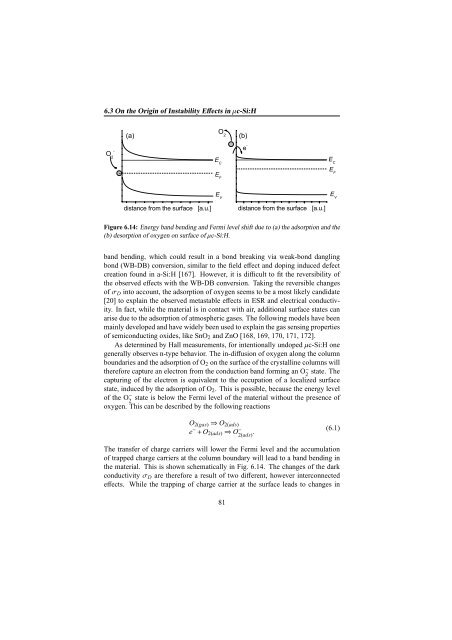
Figure 6.14: Energy band bending and Fermi level shift due to (a) the adsorption and the<br />
(b) desorption of oxygen on surface of µc-Si:H.<br />
band bending, which could result in a bond breaking via weak-bond dangling<br />
bond (WB-DB) conversion, similar to the field effect and doping induced defect<br />
creation found in a-Si:H [167]. However, it is difficult to fit the reversibility of<br />
the observed effects with the WB-DB conversion. Taking the reversible changes<br />
of σ D into account, the adsorption of oxygen seems to be a most likely candidate<br />
[20] to explain the observed metastable effects in ESR and electrical conductivity.<br />
In fact, while the material is in contact with air, additional surface states can<br />
arise due to the adsorption of atmospheric gases. The following models have been<br />
mainly developed and have widely been used to explain the gas sensing properties<br />
of semiconducting oxides, like SnO 2 and ZnO [168, 169, 170, 171, 172].<br />
As determined by Hall measurements, for intentionally undoped µc-Si:H one<br />
generally observes n-type behavior. The in-diffusion of oxygen along the column<br />
boundaries and the adsorption of O 2 on the surface of the crystalline columns will<br />
therefore capture an electron from the conduction band forming an O − 2<br />
state. The<br />
capturing of the electron is equivalent to the occupation of a localized surface<br />
state, induced by the adsorption of O 2 . This is possible, because the energy level<br />
of the O − 2<br />
state is below the Fermi level of the material without the presence of<br />
oxygen. This can be described by the following reactions<br />
O 2(gas) ⇒ O 2(ads)<br />
e − + O 2(ads) ⇒ O − 2(ads) . (6.1)<br />
The transfer of charge carriers will lower the Fermi level and the accumulation<br />
of trapped charge carriers at the column boundary will lead to a band bending in<br />
the material. This is shown schematically in Fig. 6.14. The changes of the dark<br />
conductivity σ D are therefore a result of two different, however interconnected<br />
effects. While the trapping of charge carrier at the surface leads to changes in<br />
81


