

Measurements
Electron Spin Resonance and Transient Photocurrent ... - JuSER
Electron Spin Resonance and Transient Photocurrent ... - JuSER
- No tags were found...

Create successful ePaper yourself
Turn your PDF publications into a flip-book with our unique Google optimized e-Paper software.
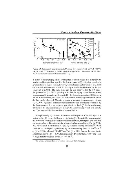
Chapter 4: Intrinsic Microcrystalline Silicon<br />
Figure 4.5: Spin density as a function of IC<br />
RS for µc-Si:H prepared with (a) VHF-PECVD<br />
and (b) HWCVD deposited at various substrate temperatures. The values for the VHF-<br />
PECVD material were taken from reference [17].<br />
in a shift of the average g-value 1 with respect to lower values. For material with<br />
no discernable crystalline signal in the Raman spectra (IC<br />
RS = 0, right panel), the<br />
g-value shifts to higher values, however, without reaching the value of g=2.0055<br />
characteristically observed in a-Si:H. The signal is clearly dominated by the resonance<br />
at g=2.0052. The same trend can be also observed for the HW material<br />
prepared at T S = 285 ◦ C (see Fig. 4.4). For the highly crystalline and amorphous<br />
material the spectra are dominated by the db 2 resonance at g=2.0052, while<br />
for the material at the µc-Si:H/a-Si:H transition an increasing contribution of the<br />
db 1 line can be observed. Material prepared at substrate temperatures as high as<br />
T S = 330 ◦ C, regardless of the structure composition all spectra are dominated by<br />
the db 2 resonance. It is important to note, that for a fixed IC<br />
RS the increasing contribution<br />
of the db 2 resonance goes along with an increasing overall spin density<br />
N S . This issue will be discussed in more detail below.<br />
The spin density N S obtained from numerical integration of the ESR spectra is<br />
plotted in Fig. 4.5 versus the Raman crystallinity IC<br />
RS . Remarkably, independent of<br />
the deposition technique and deposition conditions used, the highest spin densities<br />
are always observed for the material with the highest crystallinity. For the VHF-<br />
PECVD material, plotted in Fig. 4.5 (a), N S decreases slightly between IC RS = 0.78<br />
and 0.39. At the highest crystallinity, N S increases steeply from 2.5 × 10 16 cm −3<br />
at IC<br />
RS = 0.78 to values of 7.2 × 1016 cm −3 at IC<br />
RS = 0.80. Beyond the transition to<br />
amorphous growth (IC<br />
RS < 0.39), the spin density drops further down by one order<br />
of magnitude to values as low as 2 × 10 15 cm −3 .<br />
1 The average g-value is defined as the zero-crossing of the ESR signal.<br />
44


