

Measurements
Electron Spin Resonance and Transient Photocurrent ... - JuSER
Electron Spin Resonance and Transient Photocurrent ... - JuSER
- No tags were found...

You also want an ePaper? Increase the reach of your titles
YUMPU automatically turns print PDFs into web optimized ePapers that Google loves.
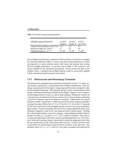
7.5 Discussion<br />
Table 7.2: Multiple trapping fitting parameters<br />
Multiple trapping Parameter µc-Si:H µc-Si:H a-Si:H<br />
sample C sample D ref. [142]<br />
Valence band mobility µ 0 [cm 2 /Vs] 1.0 2.3 0.7<br />
Band-tail width ∆E V [meV ] 31 32 45<br />
Attempt-frequency ν [s −1 ] 9× 10 8 5 × 10 9 1 × 10 12<br />
time-of-flight measurements, estimation of drift mobilities is best done in samples<br />
for which the depletion width d w is close to the physical layer thickness d i , which<br />
corresponds to a nearly uniform electric field across the intrinsic layer during<br />
the time-of-flight experiment. As can been seen in table 7.1 this criterion is not<br />
always fulfilled for the specimens investigated. In this section, the data of the<br />
samples where a standard time-of-flight analysis could be successfully applied<br />
will be summarized and discussed in more detail.<br />
7.5.1 Photocurrent and Photocharge Transients<br />
The photocurrent and photocharge transients presented in section 7.2.2 show several<br />
features expected for a conventional time-of-flight interpretation. First, the<br />
charge measurements for the higher voltages approach the same asymptotic value<br />
for the total photocharge Q 0 . This indicates that Q 0 is likely a good estimate of the<br />
charge of photogenerated holes and that for the higher voltages no loss of photoexcited<br />
charge carriers occurs, e.g. due to deep trapping. Plotting the currents on<br />
a log-log scale, the photocurrent decays consist of two linear branches, indicating<br />
a power-law behavior typical for dispersive transport. Additionally, the current<br />
transients exhibit ”transit times” (where the power-law decay steepens markedly)<br />
varying from about 500 ns (for 0.5 V) to 70 ns (for 4 V). Even the 0 V transient<br />
has the form expected for time-of-flight, but does not have the correct asymptotic<br />
photo-charge. It seems reasonable that for 0V bias voltage applied the holes were<br />
ultimately trapped by deep levels (not band-tail states) during transit. Plotting<br />
the collected photocharge versus the voltages, a deep-trapping mobility-lifetime<br />
product for holes µτ h,t of about 1 × 10 −7 cm 2 V could be evaluated. This value is<br />
in quite good agreement with earlier reports from Brueggemann et al. [23]; however,<br />
Juška and coworkers found a value which is about one magnitude lower than<br />
the one reported here [178]. These Hecht plots (see Fig. 7.4) have also been used<br />
to determine the internal field caused by the pin structure of the specimen. The<br />
obtained values of V int = 0.3 V and 0.4 V are quite reasonable and expected for<br />
97


