Optocoupler Phototransistor Output with Base Connection
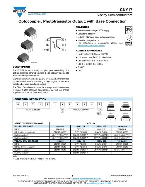
CNY17 Optocoupler, Phototransistor Output, with Base Connection
CNY17 Optocoupler, Phototransistor Output, with Base Connection
- No tags were found...

Create successful ePaper yourself
Turn your PDF publications into a flip-book with our unique Google optimized e-Paper software.
www.vishay.com<br />
CNY17<br />
Vishay Semiconductors<br />
<strong>Optocoupler</strong>, <strong>Phototransistor</strong> <strong>Output</strong>, <strong>with</strong> <strong>Base</strong> <strong>Connection</strong><br />
FEATURES<br />
• Isolation test voltage: 5000 V RMS<br />
• Long term stability<br />
• Industry standard dual-in-line package<br />
A<br />
C<br />
1<br />
2<br />
6<br />
5<br />
B<br />
C<br />
• Material categorization:<br />
For definitions of compliance please see<br />
www.vishay.com/doc?99912<br />
DESCRIPTION<br />
i179004-14<br />
The CNY17 is an optically coupled pair consisting of a<br />
gallium arsenide infrared emitting diode optically coupled to<br />
a silicon NPN phototransitor.<br />
Signal information, including a DC level, can be transmitted<br />
by the device while maintaining a high degree of electrical<br />
isolation between input and output.<br />
The CNY17 can be used to replace relays and transformers<br />
in many digital interface applications, as well as analog<br />
applications such as CRT modulation.<br />
NC<br />
3<br />
4<br />
E<br />
AGENCY APPROVALS<br />
• Underwriters lab file no. E52744<br />
• cUL tested to CSA 22.2 bulletin 5A<br />
• DIN EN 60747-5-5 (VDE 0884-5)<br />
• BSI IEC 60950, IEC 60065<br />
•FIMKO<br />
•CQC<br />
ORDERING INFORMATION<br />
C N Y 1 7 - # X 0 # # T<br />
DIP-6<br />
Option 6<br />
PART NUMBER<br />
CTR<br />
BIN<br />
PACKAGE OPTION TAPE<br />
AND<br />
REEL<br />
7.62 mm 10.16 mm<br />
Option 7<br />
Option 9<br />
> 8 mm 8 mm typ.<br />
AGENCY CERTIFIED/PACKAGE CTR (%)<br />
UL, cUL, BSI, FIMKO 40 to 80 63 to 125 100 to 200 160 to 320<br />
DIP-6 CNY17-1 CNY17-2 CNY17-3 CNY17-4<br />
DIP-6, 400 mil, option 6 CNY17-1X006 CNY17-2X006 CNY17-3X006 CNY17-4X006<br />
SMD-6, option 7 CNY17-1X007T (1) CNY17-2X007T (1) CNY17-3X007T (1) CNY17-4X007T (1)<br />
SMD-6, option 9 CNY17-1X009T (1) CNY17-2X009T (1) CNY17-3X009T (1) CNY17-4X009T (1)<br />
VDE, UL, CUL, BSI, FIMKO 40 to 80 63 to 125 100 to 200 160 to 320<br />
DIP-6 CNY17-1X001 CNY17-2X001 CNY17-3X001 CNY17-4X001<br />
DIP-6, 400 mil, option 6 CNY17-1X016 CNY17-2X016 CNY17-3X016 CNY17-4X016<br />
SMD-64, option 7 CNY17-1X017 CNY17-2X017T (1) CNY17-3X017T (1) CNY17-4X017T (1)<br />
SMD-6, option 9 - CNY17-2X019T (1) - -<br />
Note<br />
(1) Also available in tubes, do not put T on the end.<br />
Rev. 1.9, 25-Oct-12 1 Document Number: 83606<br />
For technical questions, contact: optocoupleranswers@vishay.com<br />
THIS DOCUMENT IS SUBJECT TO CHANGE WITHOUT NOTICE. THE PRODUCTS DESCRIBED HEREIN AND THIS DOCUMENT<br />
ARE SUBJECT TO SPECIFIC DISCLAIMERS, SET FORTH AT www.vishay.com/doc?91000
www.vishay.com<br />
CNY17<br />
Vishay Semiconductors<br />
ABSOLUTE MAXIMUM RATINGS (T amb = 25 °C, unless otherwise specified)<br />
PARAMETER TEST CONDITION SYMBOL VALUE UNIT<br />
INPUT<br />
Reverse voltage V R 6 V<br />
Forward current I F 60 mA<br />
Forward surge current t p ≤ 10 μs I FSM 2.5 A<br />
LED power dissipation at 25 °C P diss 70 mW<br />
OUTPUT<br />
Collector emitter breakdown voltage BV CEO 70 V<br />
Emitter base breakdown voltage BV EBO 7 V<br />
Collector current<br />
I C 50 mA<br />
t p /T = 0.5, t p ≤ 10 ms I C 100 mA<br />
Power dissipation P diss 150 mW<br />
COUPLER<br />
Isolation test voltage between emitter and detector t = 1 s V ISO 5000 V RMS<br />
Creepage distance ≥ 7 mm<br />
Clearance distance ≥ 7 mm<br />
Isolation thickness between emitter and detector ≥ 0.4 mm<br />
Comparative tracking index per<br />
DIN IEC 112/VDE 0303, part 1<br />
≥ 175<br />
Isolation resistance<br />
V IO = 500 V, T amb = 25 °C R IO ≥ 10 12 Ω<br />
V IO = 500 V, T amb = 100 °C R IO ≥ 10 11 Ω<br />
Storage temperature T stg - 55 to + 150 °C<br />
Operating temperature T amb - 55 to + 110 °C<br />
Soldering temperature (1) 2 mm from case, ≤ 10 s T sld 260 °C<br />
Total power dissipation P diss 220 mW<br />
Notes<br />
• Stresses in excess of the absolute maximum ratings can cause permanent damage to the device. Functional operation of the device is not<br />
implied at these or any other conditions in excess of those given in the operational sections of this document. Exposure to absolute<br />
maximum ratings for extended periods of the time can adversely affect reliability.<br />
(1) Refer to reflow profile for soldering conditions for surface mounted devices (SMD). Refer to wave profile for soldering conditions for through<br />
hole devices (DIP).<br />
ELECTRICAL CHARACTERISTICS (T amb = 25 °C, unless otherwise specified)<br />
PARAMETER TEST CONDITION PART SYMBOL MIN. TYP. MAX. UNIT<br />
INPUT<br />
Forward voltage I F = 60 mA V F 1.39 1.65 V<br />
Breakdown voltage I R = 10 μA V BR 6 V<br />
Reverse current V R = 6 V I R 0.01 10 μA<br />
Capacitance V R = 0 V, f = 1 MHz C O 25 pF<br />
Thermal resistance R th 750 K/W<br />
OUTPUT<br />
Collector emitter capacitance V CE = 5 V, f = 1 MHz C CE 5.2 pF<br />
Collector base capacitance V CE = 5 V, f = 1 MHz C CB 6.5 pF<br />
Emitter base capacitance V CE = 5 V, f = 1 MHz C EB 7.5 pF<br />
Thermal resistance R th 500 K/W<br />
COUPLER<br />
Collector emitter, saturation voltage V F = 10 mA, I C = 2.5 mA V CEsat 0.25 0.4 V<br />
Coupling capacitance C C 0.6 pF<br />
CNY17-1 I CEO 2 50 nA<br />
Collector emitter, leakage current<br />
V CE = 10 V<br />
CNY17-2 I CEO 2 50 nA<br />
CNY17-3 I CEO 5 100 nA<br />
CNY17-4 I CEO 5 100 nA<br />
Note<br />
• Minimum and maximum values were tested requierements. Typical values are characteristics of the device and are the result of engineering<br />
evaluations. Typical values are for information only and are not part of the testing requirements.<br />
Rev. 1.9, 25-Oct-12 2 Document Number: 83606<br />
For technical questions, contact: optocoupleranswers@vishay.com<br />
THIS DOCUMENT IS SUBJECT TO CHANGE WITHOUT NOTICE. THE PRODUCTS DESCRIBED HEREIN AND THIS DOCUMENT<br />
ARE SUBJECT TO SPECIFIC DISCLAIMERS, SET FORTH AT www.vishay.com/doc?91000
www.vishay.com<br />
CNY17<br />
Vishay Semiconductors<br />
CURRENT TRANSFER RATIO (T amb = 25 °C, unless otherwise specified)<br />
PARAMETER TEST CONDITION PART SYMBOL MIN. TYP. MAX. UNIT<br />
CNY17-1 CTR 40 80 %<br />
V CE = 5 V, I F = 10 mA<br />
CNY17-2 CTR 63 125 %<br />
CNY17-3 CTR 100 200 %<br />
I C /I F<br />
CNY17-4 CTR 160 320 %<br />
CNY17-1 CTR 13 30 %<br />
V CE = 5 V, I F = 1 mA<br />
CNY17-2 CTR 22 45 %<br />
CNY17-3 CTR 34 70 %<br />
CNY17-4 CTR 56 90 %<br />
SWITCHING CHARACTERISTICS (T amb = 25 °C, unless otherwise specified)<br />
PARAMETER TEST CONDITION PART SYMBOL MIN. TYP. MAX. UNIT<br />
LINEAR OPERATION (<strong>with</strong>out saturation)<br />
Turn-on time I F = 10 mA, V CC = 5 V, R L = 75 Ω t on 3 μs<br />
Rise time I F = 10 mA, V CC = 5 V, R L = 75 Ω t r 2 μs<br />
Turn-off time I F = 10 mA, V CC = 5 V, R L = 75 Ω t off 2.3 μs<br />
Fall time I F = 10 mA, V CC = 5 V, R L = 75 Ω t f 2 μs<br />
Cut-off frequency I F = 10 mA, V CC = 5 V, R L = 75 Ω f CO 110 kHz<br />
SWITCHING OPERATION (<strong>with</strong> saturation)<br />
I F = 20 mA CNY17-1 t on 3 μs<br />
Turn-on time<br />
I F = 10 mA<br />
CNY17-2 t on 4.2 μs<br />
CNY17-3 t on 4.2 μs<br />
I F = 5 mA CNY17-4 t on 6 μs<br />
I F = 20 mA CNY17-1 t r 2 μs<br />
Rise time<br />
I F = 10 mA<br />
CNY17-2 t r 3 μs<br />
CNY17-3 t r 3 μs<br />
I F = 5 mA CNY17-4 t r 4.6 μs<br />
I F = 20 mA CNY17-1 t off 18 μs<br />
Turn-off time<br />
I F = 10 mA<br />
CNY17-2 t off 23 μs<br />
CNY17-3 t off 23 μs<br />
I F = 5 mA CNY17-4 t off 25 μs<br />
I F = 20 mA CNY17-1 t f 11 μs<br />
Fall time<br />
I F = 10 mA<br />
CNY17-2 t f 14 μs<br />
CNY17-3 t f 14 μs<br />
I F = 5 mA CNY17-4 t f 15 μs<br />
I F I F<br />
+ 5 V<br />
0<br />
R G = 50 Ω<br />
t p<br />
T = 0.01 t p = 50 µs<br />
I F<br />
I C<br />
0<br />
100 %<br />
90 %<br />
t p<br />
95 10804-3<br />
50 Ω R L<br />
Channel I<br />
Channel II<br />
Oscilloscope<br />
R L = 1 MΩ<br />
C L = 20 pF<br />
Fig. 1 - Test Circuit, Non-Saturated Operation<br />
I F I F = 10 mA + 5 V<br />
0<br />
I C<br />
R G = 50 Ω<br />
t p<br />
T = 0.01 t p = 50 µs<br />
10 %<br />
0<br />
t p<br />
t d<br />
t r<br />
t on (= t d + t r )<br />
t r<br />
t d<br />
t on<br />
t s<br />
t f<br />
t off<br />
Pulse duration<br />
Delay time<br />
Rise time<br />
Turn-on time<br />
t s<br />
t f<br />
t off (= t s + t f )<br />
Fig. 3 - Switching Times<br />
t<br />
t<br />
Storage time<br />
Fall time<br />
Turn-off time<br />
96 11698<br />
50 Ω 1 kΩ<br />
Channel I<br />
Channel II<br />
Oscilloscope<br />
R L ≥ 1 MΩ<br />
C L ≤ 20 pF<br />
95 10843<br />
Fig. 2 - Test Circuit, Saturated Operation<br />
Rev. 1.9, 25-Oct-12 3 Document Number: 83606<br />
For technical questions, contact: optocoupleranswers@vishay.com<br />
THIS DOCUMENT IS SUBJECT TO CHANGE WITHOUT NOTICE. THE PRODUCTS DESCRIBED HEREIN AND THIS DOCUMENT<br />
ARE SUBJECT TO SPECIFIC DISCLAIMERS, SET FORTH AT www.vishay.com/doc?91000
www.vishay.com<br />
CNY17<br />
Vishay Semiconductors<br />
TYPICAL CHARACTERISTICS (T amb = 25 °C, unless otherwise specified)<br />
V F - Forward Voltage (V)<br />
1.8<br />
1.7<br />
1.6<br />
T amb = 0 °C<br />
1.5<br />
T amb = - 25 °C<br />
1.4<br />
T amb = - 40 °C<br />
1.3 T amb = - 55 °C<br />
1.2<br />
1.1<br />
1.0<br />
T amb = 25 °C<br />
0.9<br />
T amb = 50 °C<br />
0.8<br />
T amb = 75 °C<br />
0.7<br />
T amb = 100 °C<br />
0.6<br />
0.1 1 10 100<br />
I F - Forward Current (mA)<br />
I CE0 - Leakage Current (nA)<br />
10 000<br />
I F = 0 mA<br />
1000<br />
V CE = 40 V<br />
100<br />
10<br />
1<br />
V CE = 24 V<br />
V CE = 12 V<br />
0.1<br />
0.01<br />
0.001<br />
- 60 - 40 - 20 0 20 40 60 80 100<br />
T amb - Ambient Temperature (°C)<br />
Fig. 4 - Forward Voltage vs. Forward Current<br />
Fig. 7 - Leakage Current vs. Ambient Temperature<br />
I C - Collector Current (mA)<br />
60<br />
50<br />
40<br />
30<br />
20<br />
10<br />
I F = 30 mA<br />
I F = 20 mA<br />
I F = 15 mA<br />
I F = 10 mA<br />
I F = 5 mA<br />
CTR Norm - Normalized CTR (NS)<br />
1.2<br />
1.0<br />
0.8<br />
0.6<br />
0.4<br />
0.2<br />
I F = 10 mA<br />
I F = 5 mA<br />
I F = 1 mA<br />
V CE = 5 V<br />
0<br />
0 1 2 3 4 5 6 7 8<br />
V CE - Collector Emitter Voltage (NS) (V)<br />
0<br />
- 60 - 40 - 20 0 20 40 60 80 100<br />
T amb - Ambient Temperature (°C)<br />
Fig. 5 - Collector Current vs. Collector Emitter Voltage (NS)<br />
Fig. 8 - Normalized CTR (NS) vs. Ambient Temperature<br />
I C - Collector Current (mA)<br />
25<br />
20<br />
15<br />
10<br />
5<br />
I F = 1 mA<br />
I F = 25 mA<br />
I F = 10 mA<br />
I F = 5 mA<br />
I F = 2 mA<br />
CTR Norm - Normalized CTR (sat)<br />
1.2<br />
1.0<br />
0.8<br />
0.6<br />
0.4<br />
0.2<br />
I F = 10 mA<br />
I F = 5 mA<br />
I F = 1 mA<br />
V CE = 0.4 V<br />
0<br />
0 0.1 0.2 0.3 0.4<br />
V CE - Collector Emitter Voltage (sat) (V)<br />
0<br />
- 60 - 40 - 20 0 20 40 60 80 100<br />
T amb - Ambient Temperature (°C)<br />
Fig. 6 - Collector Current vs. Collector Emitter Voltage (sat)<br />
Fig. 9 - Normalized CTR (sat) vs. Ambient Temperature<br />
Rev. 1.9, 25-Oct-12 4 Document Number: 83606<br />
For technical questions, contact: optocoupleranswers@vishay.com<br />
THIS DOCUMENT IS SUBJECT TO CHANGE WITHOUT NOTICE. THE PRODUCTS DESCRIBED HEREIN AND THIS DOCUMENT<br />
ARE SUBJECT TO SPECIFIC DISCLAIMERS, SET FORTH AT www.vishay.com/doc?91000
www.vishay.com<br />
CNY17<br />
Vishay Semiconductors<br />
CTR Norm - Normalized CTR (NS)<br />
1.2<br />
V CE = 5 V<br />
1.0<br />
T amb = 25 °C<br />
T amb = 0 °C<br />
0.8 T amb = - 40 °C<br />
0.6<br />
T amb = - 55 °C<br />
0.4<br />
T amb = 50 °C<br />
T amb = 75 °C<br />
0.2<br />
T amb = 100 °C<br />
0<br />
0.1 1 10 100<br />
I F - Forward Current (mA)<br />
f CTR - CTR Frequency (kHz)<br />
1000<br />
V CC = 5 V<br />
100<br />
10<br />
1<br />
0.1 1 10 100<br />
I C - Collector Current (mA)<br />
Fig. 10 - Normalized CTR (NS) vs. Forward Current<br />
Fig. 13 - CTR Frequency vs. Collector Current<br />
CTR Norm - Normalized CTR (sat)<br />
1.2<br />
V CE = 0.4 V<br />
1.0<br />
T amb = 25 °C<br />
T amb = 0 °C<br />
0.8 T amb = - 40 °C<br />
T amb = - 55 °C<br />
0.6<br />
0.4<br />
T amb = 50 °C<br />
T amb = 75 °C<br />
0.2<br />
T amb = 100 °C<br />
0<br />
0.1 1 10 100<br />
I F - Forward Current (mA)<br />
t on , t off - Switching Time (μs)<br />
1000<br />
V CE = 5 V, I F = 10 mA<br />
100<br />
10<br />
t off<br />
t on<br />
1<br />
0.1<br />
0.1 1 10 100<br />
R L - Load Resistance (kΩ)<br />
Fig. 11 - Normalized CTR (sat) vs. Forward Current<br />
Fig. 14 - Switching Time vs. Load Resistance<br />
0<br />
- 20<br />
V CE = 5 V<br />
Phase (deg)<br />
- 40<br />
- 60<br />
- 80<br />
- 100<br />
- 120<br />
- 140<br />
- 160<br />
1 10 100 1000<br />
f - Frequency (kHz)<br />
Fig. 12 - CTR Frequency vs. Phase Angle<br />
Rev. 1.9, 25-Oct-12 5 Document Number: 83606<br />
For technical questions, contact: optocoupleranswers@vishay.com<br />
THIS DOCUMENT IS SUBJECT TO CHANGE WITHOUT NOTICE. THE PRODUCTS DESCRIBED HEREIN AND THIS DOCUMENT<br />
ARE SUBJECT TO SPECIFIC DISCLAIMERS, SET FORTH AT www.vishay.com/doc?91000
www.vishay.com<br />
CNY17<br />
Vishay Semiconductors<br />
PACKAGE DIMENSIONS in millimeters<br />
6 5 4<br />
6.5 ± 0.5<br />
1 2 3<br />
7.3 ± 0.5<br />
7.62 ± 0.3<br />
1.1 ± 0.1<br />
3.5 ± 0.3<br />
0.5 typ.<br />
2.8 ± 0.5<br />
3.3 ± 0.5<br />
22530<br />
2.54 ± 0.25<br />
0.5 ± 0.1<br />
0.26<br />
7.62 to 9.98<br />
Option 6<br />
Option 7 Option 9<br />
7.62 typ.<br />
7.62 typ.<br />
7.62 typ.<br />
3.5 ± 0.3<br />
0.35 ± 0.25<br />
3.5 ± 0.3<br />
0.1 ± 0.1 3.5 ± 0.3<br />
0.1 min.<br />
0.6 min.<br />
2.7 min. 8 min.<br />
0.6 min. 8.16 ± 0.8<br />
10.16 typ.<br />
10.3 max.<br />
10.16 ± 0.3<br />
0.76<br />
0.76<br />
2.54<br />
R 0.25<br />
1.78<br />
2.54<br />
R 0.25<br />
1.78<br />
20802-34<br />
8 min.<br />
11.05<br />
1.52<br />
8 min.<br />
11.05<br />
1.52<br />
PACKAGE MARKING<br />
CNY17-3<br />
Pin 1 I.D.<br />
V YWW 25<br />
Notes<br />
• VDE logo is only marked on option 1 parts. Option information is not marked on the part.<br />
• Tape and reel suffix (T) is not part of the package marking.<br />
Rev. 1.9, 25-Oct-12 6 Document Number: 83606<br />
For technical questions, contact: optocoupleranswers@vishay.com<br />
THIS DOCUMENT IS SUBJECT TO CHANGE WITHOUT NOTICE. THE PRODUCTS DESCRIBED HEREIN AND THIS DOCUMENT<br />
ARE SUBJECT TO SPECIFIC DISCLAIMERS, SET FORTH AT www.vishay.com/doc?91000
www.vishay.com<br />
CNY17<br />
Vishay Semiconductors<br />
TUBE AND TAPE INFORMATION<br />
DEVICES PER TUBE<br />
TYPE UNITS/TUBE TUBES/BOX UNITS/BOX<br />
DIP-6 50 40 2000<br />
Ø 1.55 ± 0.05 2 ± 0.1 4 ± 0.1<br />
1.75 ± 0.1<br />
7.5 ± 0.1<br />
16 ± 0.3<br />
12 ± 0.1<br />
0.3 ± 0.05<br />
22537-1<br />
Fig. 15 - Tape and Reel Drawing, 1000 Units per Reel<br />
Rev. 1.9, 25-Oct-12 7 Document Number: 83606<br />
For technical questions, contact: optocoupleranswers@vishay.com<br />
THIS DOCUMENT IS SUBJECT TO CHANGE WITHOUT NOTICE. THE PRODUCTS DESCRIBED HEREIN AND THIS DOCUMENT<br />
ARE SUBJECT TO SPECIFIC DISCLAIMERS, SET FORTH AT www.vishay.com/doc?91000
www.vishay.com<br />
Legal Disclaimer Notice<br />
Vishay<br />
Disclaimer<br />
ALL PRODUCT, PRODUCT SPECIFICATIONS AND DATA ARE SUBJECT TO CHANGE WITHOUT NOTICE TO IMPROVE<br />
RELIABILITY, FUNCTION OR DESIGN OR OTHERWISE.<br />
Vishay Intertechnology, Inc., its affiliates, agents, and employees, and all persons acting on its or their behalf (collectively,<br />
“Vishay”), disclaim any and all liability for any errors, inaccuracies or incompleteness contained in any datasheet or in any other<br />
disclosure relating to any product.<br />
Vishay makes no warranty, representation or guarantee regarding the suitability of the products for any particular purpose or<br />
the continuing production of any product. To the maximum extent permitted by applicable law, Vishay disclaims (i) any and all<br />
liability arising out of the application or use of any product, (ii) any and all liability, including <strong>with</strong>out limitation special,<br />
consequential or incidental damages, and (iii) any and all implied warranties, including warranties of fitness for particular<br />
purpose, non-infringement and merchantability.<br />
Statements regarding the suitability of products for certain types of applications are based on Vishay’s knowledge of typical<br />
requirements that are often placed on Vishay products in generic applications. Such statements are not binding statements<br />
about the suitability of products for a particular application. It is the customer’s responsibility to validate that a particular<br />
product <strong>with</strong> the properties described in the product specification is suitable for use in a particular application. Parameters<br />
provided in datasheets and/or specifications may vary in different applications and performance may vary over time. All<br />
operating parameters, including typical parameters, must be validated for each customer application by the customer’s<br />
technical experts. Product specifications do not expand or otherwise modify Vishay’s terms and conditions of purchase,<br />
including but not limited to the warranty expressed therein.<br />
Except as expressly indicated in writing, Vishay products are not designed for use in medical, life-saving, or life-sustaining<br />
applications or for any other application in which the failure of the Vishay product could result in personal injury or death.<br />
Customers using or selling Vishay products not expressly indicated for use in such applications do so at their own risk. Please<br />
contact authorized Vishay personnel to obtain written terms and conditions regarding products designed for such applications.<br />
No license, express or implied, by estoppel or otherwise, to any intellectual property rights is granted by this document or by<br />
any conduct of Vishay. Product names and markings noted herein may be trademarks of their respective owners.<br />
Material Category Policy<br />
Vishay Intertechnology, Inc. hereby certifies that all its products that are identified as RoHS-Compliant fulfill the<br />
definitions and restrictions defined under Directive 2011/65/EU of The European Parliament and of the Council<br />
of June 8, 2011 on the restriction of the use of certain hazardous substances in electrical and electronic equipment<br />
(EEE) - recast, unless otherwise specified as non-compliant.<br />
Please note that some Vishay documentation may still make reference to RoHS Directive 2002/95/EC. We confirm that<br />
all the products identified as being compliant to Directive 2002/95/EC conform to Directive 2011/65/EU.<br />
Vishay Intertechnology, Inc. hereby certifies that all its products that are identified as Halogen-Free follow Halogen-Free<br />
requirements as per JEDEC JS709A standards. Please note that some Vishay documentation may still make reference<br />
to the IEC 61249-2-21 definition. We confirm that all the products identified as being compliant to IEC 61249-2-21<br />
conform to JEDEC JS709A standards.<br />
Revision: 02-Oct-12 1 Document Number: 91000

![1RUPDOQH \FLHFKU]H FLMD VNLH](https://img.yumpu.com/54031532/1/184x260/1rupdoqh-flhfkuh-flmd-vnlh.jpg?quality=85)