

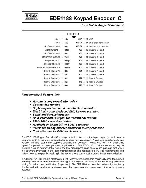
EDE1188 Keypad Encoder IC
EDE1188 Keypad Encoder IC - SingleChips
EDE1188 Keypad Encoder IC - SingleChips

You also want an ePaper? Increase the reach of your titles
YUMPU automatically turns print PDFs into web optimized ePapers that Google loves.
<strong>EDE1188</strong> <strong>Keypad</strong> <strong>Encoder</strong> <strong>IC</strong><br />
8 x 8 Matrix <strong>Keypad</strong> <strong>Encoder</strong> <strong>IC</strong><br />
Functionality & Feature Set:<br />
• Automatic key repeat after delay<br />
• Contact debouncing<br />
• Keybeep provides tactile feedback to operator<br />
• Electrically quiet (reduced EMI) keypad scanning<br />
• Serial and Parallel outputs<br />
• Data Valid output signal for interrupt activation<br />
• 2400/ 9600 serial Baud rates<br />
• Available in 28 pin DIP or SO<strong>IC</strong> packages<br />
• Interfaces to any microcontroller or microprocessor<br />
• Cost effective for OEM applications<br />
The <strong>EDE1188</strong> <strong>Keypad</strong> <strong>Encoder</strong> <strong>IC</strong> is designed to interface a matrix-type keypad (up to 8 rows x 8<br />
columns, or 64 keys) to a microcontroller or other host processor. A one-wire serial or eight-wire<br />
parallel interface returns the keypress data and can be used in conjunction with the 'Data Valid'<br />
signal for polled or interrupt-driven applications. The <strong>EDE1188</strong> provides enhanced keypad<br />
features such as contact debouncing and key auto-repeat in an easy-to-use package that lowers<br />
the software overhead in the host microcontroller and reduces the I/O pin requirements from<br />
sixteen to one, frequently resulting in the use of a less costly host microcontroller in your design.<br />
In addition, the <strong>EDE1188</strong> is electrically quiet. Many keypad encoders continually scan the keypad,<br />
radiating EMI noise from the wires leading to the keypad (resulting in trouble during emissions<br />
testing & final product certification & approval). The <strong>EDE1188</strong> reduces this problem by monitoring<br />
the keypad with unchanging signals, and then scanning only once each time a keypress is<br />
detected.<br />
Copyright © 2002 E-Lab Digital Engineering, Inc. All Rights Reserved. Page 1/8
<strong>EDE1188</strong> <strong>Keypad</strong> <strong>Encoder</strong> <strong>IC</strong><br />
PIN DEFINITIONS<br />
<strong>Keypad</strong> Connection Pins:<br />
(R0) Row 0 / Data 0 Output (Pin 10)........................................Multiplexed <strong>Keypad</strong> Row 0, Host System Data Input 0<br />
(R1) Row 1 / Data 1 Output (Pin 11)........................................Multiplexed <strong>Keypad</strong> Row 1, Host System Data Input 1<br />
(R2) Row 2 / Data 2 Output (Pin 12)........................................Multiplexed <strong>Keypad</strong> Row 2, Host System Data Input 2<br />
(R3) Row 3 / Data 3 Output (Pin 13)........................................Multiplexed <strong>Keypad</strong> Row 3, Host System Data Input 3<br />
(R4) Row 4 / Data 4 Output (Pin 14)........................................Multiplexed <strong>Keypad</strong> Row 4, Host System Data Input 4<br />
(R5) Row 5 / Data 5 Output (Pin 15)........................................Multiplexed <strong>Keypad</strong> Row 5, Host System Data Input 5<br />
(R6) Row 6 / Data 6 Output (Pin 16)........................................Multiplexed <strong>Keypad</strong> Row 6, Host System Data Input 6<br />
(R7) Row 7 / Data 7 Output (Pin 17)........................................Multiplexed <strong>Keypad</strong> Row 7, Host System Data Input 7<br />
(C0) Column 0 Input (Pin 18)...............................................…Multiplexed <strong>Keypad</strong> Column 0 (through 330 O resistor)<br />
(C1) Column 1 Input (Pin 19)...............................................…Multiplexed <strong>Keypad</strong> Column 1 (through 330 O resistor)<br />
(C2) Column 2 Input (Pin 20)...............................................…Multiplexed <strong>Keypad</strong> Column 2 (through 330 O resistor)<br />
(C3) Column 3 Input (Pin 21)...............................................…Multiplexed <strong>Keypad</strong> Column 3 (through 330 O resistor)<br />
(C4) Column 4 Input (Pin 22)...............................................…Multiplexed <strong>Keypad</strong> Column 4 (through 330 O resistor)<br />
(C5) Column 5 Input (Pin 23)...............................................…Multiplexed <strong>Keypad</strong> Column 5 (through 330 O resistor)<br />
(C6) Column 6 Input (Pin 24)...............................................…Multiplexed <strong>Keypad</strong> Column 6 (through 330 O resistor)<br />
(C7) Column 7 Input (Pin 25)...............................................…Multiplexed <strong>Keypad</strong> Column 7 (through 330 O resistor)<br />
Control & Data Pins:<br />
Valid (Pin 6).....................................................................…...Data Valid Signal / Parallel data valid when low<br />
Beep (Pin 7)........................................................................…Modulated Output Signal: Oscillates on keypress or repeat<br />
XMIT (Pin 8)........................................................................…Serial Data Output (N-8-1); RS232 timing, TTL/CMOS<br />
Voltage<br />
Baud (Pin 9)...........................................................................Baud Rate Selection: 0=2400, 1=9600<br />
Clock / Power Pins:<br />
OSC1 (Pin 27)........................................................................One pin of 4MHz parallel-cut crystal or resonator, or a direct<br />
TTL clock input<br />
OSC2 (Pin 26)........................................................................Other pin of 4MHz parallel-cut crystal or resonator, or leave<br />
floating if OSC1 driven with a TTL clock input<br />
+5V (Pins 1,2,28)................................................................…Connect to +5V DC<br />
GND (Pin 4).........................................................................…Connect to 0V DC (Ground)<br />
Note: DIP are SO<strong>IC</strong> (surface mount) packages of the <strong>EDE1188</strong> have identical pinout.<br />
Please specify <strong>EDE1188</strong>/P (for DIP) or <strong>EDE1188</strong>/SO (for SO<strong>IC</strong>) when ordering.<br />
Page 2/8
<strong>EDE1188</strong> <strong>Keypad</strong> <strong>Encoder</strong> <strong>IC</strong><br />
Figure One: Connection Block Diagram<br />
As illustrated by Figure One, the <strong>EDE1188</strong> resides between the keypad and host microcontroller/<br />
processor. The host microcontroller receives keypress data via either the eight parallel data<br />
outputs (D0-D7, Pins 10-17) or the Serial Data Output (Pin 8). The Data Valid signal (Pin 6) is<br />
activated upon keypress (and upon each key repeat cycle if key is held). The Data Valid signal is<br />
activated prior to transmission of the serial data to allow polled (software-UART) style host serial<br />
systems such as the BAS<strong>IC</strong> Stamp or a microcontroller without a hardware UART to enter the<br />
serial receive routine and receive the keypress data without needing to continually wait for the<br />
start bit. Note that the data outputs to the host microcontroller reside on the row output pins (Pins<br />
10-17), therefore parallel-output data should only be read when the Data Valid (Pin 6) signal is<br />
active (low). Upon powerup, the eight data output pins will be high, and will remain high except<br />
when a key is pressed.<br />
Page 3/8
<strong>EDE1188</strong> <strong>Keypad</strong> <strong>Encoder</strong> <strong>IC</strong><br />
The following table illustrates the data values returned by the serial and parallel outputs of the<br />
EDE188 upon each keypress.<br />
Key Number Serial Output Parallel Output Key Number Serial Output Parallel Output<br />
1 $01 (1 decimal) 00000001 33 $21 (33 decimal) 00100001<br />
2 $02 (2 decimal) 00000010 34 $22 (34 decimal) 00100010<br />
3 $03 (3 decimal) 00000011 35 $23 (35 decimal) 00100011<br />
4 $04 (4 decimal) 00000100 36 $24 (36 decimal) 00100100<br />
5 $05 (5 decimal) 00000101 37 $25 (37 decimal) 00100101<br />
6 $06 (6 decimal) 00000110 38 $26 (38 decimal) 00100110<br />
7 $07 (7 decimal) 00000111 39 $27 (39 decimal) 00100111<br />
8 $08 (8 decimal) 00001000 40 $28 (40 decimal) 00101000<br />
9 $09 (9 decimal) 00001001 41 $29 (41 decimal) 00101001<br />
10 $0A (10 decimal) 00001010 42 $2A (42 decimal) 00101010<br />
11 $0B (11 decimal) 00001011 43 $2B (43 decimal) 00101011<br />
12 $0C (12 decimal) 00001100 44 $2C (44 decimal) 00101100<br />
13 $0D (13 decimal) 00001101 45 $2D (45 decimal) 00101101<br />
14 $0E (14 decimal) 00001110 46 $2E (46 decimal) 00101110<br />
15 $0F (15 decimal) 00001111 47 $2F (47 decimal) 00101111<br />
16 $10 (16 decimal) 00010000 48 $30 (48 decimal) 00110000<br />
17 $11 (17 decimal) 00010001 49 $31 (49 decimal) 00110001<br />
18 $12 (18 decimal) 00010010 50 $32 (50 decimal) 00110010<br />
19 $13 (19 decimal) 00010011 51 $33 (51 decimal) 00110011<br />
20 $14 (20 decimal) 00010100 52 $34 (52 decimal) 00110100<br />
21 $15 (21 decimal) 00010101 53 $35 (53 decimal) 00110101<br />
22 $16 (22 decimal) 00010110 54 $36 (54 decimal) 00110110<br />
23 $17 (23 decimal) 00010111 55 $37 (55 decimal) 00110111<br />
24 $18 (24 decimal) 00011000 56 $38 (56 decimal) 00111000<br />
25 $19 (25 decimal) 00011001 57 $39 (57 decimal) 00111001<br />
26 $1A (26 decimal) 00011010 58 $3A (58 decimal) 00111010<br />
27 $1B (27 decimal) 00011011 59 $3B (59 decimal) 00111011<br />
28 $1C (28 decimal) 00011100 60 $3C (60 decimal) 00111100<br />
29 $1D (29 decimal) 00011101 61 $3D (61 decimal) 00111101<br />
30 $1E (30 decimal) 00011110 62 $3E (62 decimal) 00111110<br />
31 $1F (31 decimal) 00011111 63 $3F (63 decimal) 00111111<br />
32 $20 (32 decimal) 00100000 64 $40 (64 decimal) 01000000<br />
Table One: Keynumber vs. Output Data<br />
OVERVIEW OF OPERATION<br />
Table One of the previous page illustrates the data that is output upon each keypress. The<br />
following sequence is initiated upon each keypress, and is repeated if the key is held:<br />
1. Keypress is detected<br />
2. One scan cycle is performed<br />
3. Parallel Outputs (D7..D0) are latched with the appropriate value<br />
4. Data Valid signal is activated (pulled low)<br />
5. Beeper (1KHz square wave) is activated for 45mS<br />
6. Serial data is transmitted<br />
Page 4/8
<strong>EDE1188</strong> <strong>Keypad</strong> <strong>Encoder</strong> <strong>IC</strong><br />
This entire cycle takes 50mS (regardless of Baud rate selected). If a key is held longer than<br />
the autorepeat delay of 660 mS, the cycle is repeated again at a rate of 5 times per second.<br />
The following timing diagram illustrates the above sequence:<br />
0ms 10ms 20ms 30ms 40ms 50ms<br />
Keypress<br />
50mS<br />
(Multiple transitions are due to contact bounce)<br />
Parallel_Outputs<br />
D7..D0 latched with appropriate value<br />
Data_Valid_Output<br />
1uS<br />
Serial_Output<br />
Beeper_Output<br />
45mS<br />
(Square wave is not to scale)<br />
Once a key is pressed, any additional closures (bounce) of that contact, or of any other contacts<br />
are ignored for 50mS, during which several signals are output by the <strong>EDE1188</strong>. First, the parallel<br />
outputs D0..D7 (Pins 10-17) are latched with the appropriate keypress value. One microsecond<br />
later, the Data Valid Output (Pin 6) goes low, indicating that there is valid data on the parallel<br />
output pins. Following this, the Beeper Output (Pin 7) pulse stream is generated for 45mS,<br />
providing auditory confirmation to the keypad operator that a key has been pressed. Finally, the<br />
RS-232 Output (Pin 8) transmits the keypress data at the Baud rate selected by the Baud rate<br />
input select (Pin 9). After this, a delay period (determined by Baud rate chosen) is waited to make<br />
the entire process to last precisely 50mS.<br />
If a key is held longer that the autorepeat delay of 660mS, the outputs are cleared and this entire<br />
process is repeated every 204mS until the key is released by the operator.<br />
Figure Two illustrates a typical connection of a 8x8 keypad to the <strong>EDE1188</strong>. Note that R0-R7<br />
(Pins 10-17) are connected to the keypad rows through 330 Ohm resistors. They are present to<br />
prevent a short circuit during the scan cycle in case more than one key is being held at a time,<br />
and they also help to lower radiated emissions from the keypad wires. The 4.7K Ohm resistors on<br />
the keypad columns are pulldowns to prevent the <strong>EDE1188</strong> column inputs from floating or<br />
oscillating. Pulldowns should be present on all eight column inputs (C0..C7) regardless of the<br />
keypad size or configuration being used. Note: Power and Ground connections have been<br />
omitted from the <strong>EDE1188</strong> hookup shown in Figure Two to simplify the illustration. They must be<br />
connected in actual operation. Also, when using a 4MHz resonator with internal capacitors, the<br />
third (center) pin should be connected to ground.<br />
Page 5/8
<strong>EDE1188</strong> <strong>Keypad</strong> <strong>Encoder</strong> <strong>IC</strong><br />
Figure Two: Schematic of <strong>Keypad</strong> Connection<br />
PARALLEL DATA CONNECTION<br />
To read data from the <strong>EDE1188</strong> in a parallel as opposed to serial format, your host<br />
microcontroller should input from the eight data inputs D0-D7, which also serve as the row drive<br />
signal pins R0-R7 (see Figure Two). While the <strong>EDE1188</strong> is waiting for a keypress, it will hold all<br />
eight lines high. Once a key is pressed, the data output pins will toggle while the keypad is<br />
scanned so that the <strong>EDE1188</strong> can determine which key was pressed. Then, the appropriate data<br />
value (see Table One) will be output onto the data outputs (the row output pins), and the Data<br />
Valid Output (Pin 6) will go low. This pin will stay low for 50 mS, during which the Data Output<br />
pins will hold the keypress data. The keypress data should be sampled during this 50mS window.<br />
Both the Parallel & Serial Data outputs are activated on each keypress (and autorepeat cycle);<br />
designers using the parallel data outputs can ignore the serial data output (and vice versa -<br />
designers using the serial data output can ignore the parallel data output).<br />
Page 6/8
<strong>EDE1188</strong> <strong>Keypad</strong> <strong>Encoder</strong> <strong>IC</strong><br />
SERIAL DATA CONNECTION<br />
To receive keypress data serially from the <strong>EDE1188</strong>, two options exist. The first (typically used<br />
with a host microcontroller having an onboard hardware UART) is to simply connect the XMIT (Pin<br />
8) line to the host microcontroller's serial data input. Each time a key is pressed (or the<br />
autorepeat loop cycles) one byte will be transmitted, corresponding to the values shown in Table<br />
One. The host microcontroller's hardware UART's 'Receive Buffer Full' flag can be polled to<br />
monitor for newly received serial data; alternately the host microcontroller can be configured to<br />
generate an interrupt when a new byte is received by the UART.<br />
The second method of receiving serial data from the <strong>EDE1188</strong> involves the use of the Data Valid<br />
signal (Pin 6). This pin can be polled by the host microcontroller, or connected to an external<br />
interrupt input. Once this pin transitions to its active level (low), the <strong>EDE1188</strong> pauses 45mS (while<br />
the keybeep signal is generated) before the start bit and remaining data bits are sent, during<br />
which the host microcontroller can finish what it is doing and enter the serial receive routine,<br />
holding there until it detects the <strong>EDE1188</strong>'s start bit. This method is ideal for BAS<strong>IC</strong> Stamps<br />
and other devices using a 'software' (a non-hardware, or 'bit-bang') UART.<br />
SMALLER KEYPADS<br />
The <strong>EDE1188</strong> can be used with keypads smaller than 8 rows by 8 columns, such as five rows by<br />
four columns, two rows by six columns, etc. Simply connect the keypad as shown in Figure Two,<br />
starting with Row 0 and Column 0, connecting as many rows and columns as your keypad has.<br />
Be certain to use the 330 Ohm resistor to connect each row of your keypad, and also be certain to<br />
pull all eight column inputs (C0..C7) to ground with eight 4.7K Ohm resistors as illustrated in<br />
Figure Two.<br />
BEEPER CONNECTION<br />
In order to provide tactile feedback to the operator, the Beeper Output (Pin 7) of the <strong>EDE1188</strong> is<br />
designed to drive a piezo beeper or speaker via a NPN transistor such as the 2N2222. Figure<br />
Two illustrates a typical common-emitter configuration. With the common-emitter drive<br />
configuration, be certain to use a resistor from the <strong>EDE1188</strong> Beeper Output (Pin 7) to the<br />
transistor's base pin to limit base drive current. Your particular beeper may or may not require a<br />
resistor in series with it to limit current. The drive signal is a 1KHz square wave, toggling from 0 to<br />
5 Volts, with a duration of 45mS.<br />
RS-232 OUTPUT<br />
The RS-232 Output (Pin 8) transmits serial data to the host microcontroller. This data is sent at<br />
either 2400 or 9600 Baud, as selected by Pin 9. Data is send in traditional N-8-1 (no parity, 8 data<br />
bits, one stop bit) format at TTL/CMOS voltage levels; i.e. 0V to 5V. This serial output signal can<br />
be connected directly to the host microcontroller's serial input pin without any type of voltage level<br />
conversion. However, if data is to be sent to a device expecting RS-232 voltage levels of -12V to<br />
+12V (such as a PC), a voltage level conversion <strong>IC</strong> such as the MAX232 will be needed between<br />
the <strong>EDE1188</strong>'s serial output pin and the PC's serial input pin.<br />
Page 7/8
<strong>EDE1188</strong> <strong>Keypad</strong> <strong>Encoder</strong> <strong>IC</strong><br />
Although we strive to maintain a high degree of technical accuracy, this document may contain typographical errors or other inaccuracies.<br />
We reserve the right to correct any inaccuracy in future editions of this document without notice. This document and examples contained<br />
herein are provided 'As Is' without warranty of any kind expressed or implied. This document is to be used for informational purposes only<br />
and may not be duplicated for commercial purposes other than by distributors authorized by E-Lab Digital Engineering, Inc.<br />
ABSOLUTE MAXIMUM RATINGS<br />
Oscillator frequency .......................................... 4 MHz<br />
Supply Voltage ................................................... 7.5V<br />
Ambient temperature under bias ...................... -55?C to +125?C<br />
Max. current sunk by an output pin .................. 25mA<br />
Max. current sourced by an output pin ............. 20mA<br />
Max. current sunk by all 4 column inputs.......... 50mA<br />
Max. current sourced by all 4 row outputs......... 40mA<br />
STANDARD OPERATING CONDITIONS<br />
Supply voltage ................................................. 4.75V to 5.25V<br />
Typical current draw......................................... 1.8mA<br />
Operating temperature ..................................... 0?C to +70?C<br />
IMPORTANT NOT<strong>IC</strong>E<br />
E-LAB Digital Engineering, Inc. (E-LAB), reserves the right to<br />
change products or specifications without notice. Customers<br />
are advised to obtain the latest versions of product<br />
specifications, which should be considered when evaluating a<br />
product’s appropriateness for a particular use.<br />
THIS PRODUCT IS WARRANTED TO COMPLY WITH E-<br />
LAB’S SPECIF<strong>IC</strong>ATION SHEET AT THE TIME OF DELIVERY.<br />
BY USING THIS PRODUCT, CUSTOMER AGREES THAT IN<br />
NO EVENT SHALL E-LAB BE LIABLE FOR ANY DIRECT,<br />
INDIRECT, SPECIAL, INCIDENTAL OR CONSEQUENTIAL<br />
DAMAGES AS A RESULT OF THE PERFORMANCE, OR<br />
FAILURE TO PERFORM, OF THIS PRODUCT.<br />
E-LAB MAKES NO OTHER WARRANTIES, EXPRESSED OR<br />
IMPLIED, INCLUDING ANY IMPLIED WARRANTIES OF<br />
MERCHANTABILITY OR FITNESS FOR A PART<strong>IC</strong>ULAR<br />
PURPOSE.<br />
E-LAB’s LIABILITY IS FOR A PERIOD NO GREATER THAN 90<br />
DAYS FROM DATE OF SHIPMENT BY E-LAB AND IS<br />
LIMITED TO REPLACEMENT OF DEFECTIVE PRODUCT.<br />
This warranty covers only defects arising under normal use and<br />
not malfunctions resulting from misuse, abuse, modification, or<br />
repairs by anyone other than E-LAB.<br />
E-LAB’S PRODUCTS ARE NOT AUTHORIZED FOR USE AS<br />
CRIT<strong>IC</strong>AL COMPONENTS IN LIFE SUPPORT DEV<strong>IC</strong>ES OR<br />
SYSTEMS WITHOUT THE EXPRESS WRITTEN APPROVAL<br />
OF THE PRESIDENT OF E-LAB. Life support devices or<br />
systems are those which are intended to support or sustain life<br />
and whose failure to perform can be reasonably expected to<br />
result in a significant injury or death to the user. Critical<br />
components are those whose failure to perform can be<br />
reasonably expected to cause failure of a life support device or<br />
system or affect its safety or effectiveness.<br />
COPYRIGHT NOT<strong>IC</strong>E<br />
This product may not be duplicated. E-LAB Digital Engineering, Inc. holds all copyrights on firmware, with all rights reserved. Unauthorized<br />
duplication of this device will be subject to penalty under state and/ or federal law.<br />
<strong>EDE1188</strong> and the E-LAB logo are trademarks of E-LAB Digital Engineering, Inc. All other trademarks and registered trademarks are<br />
property of their respective owners.<br />
CONTACTING US<br />
We are continually updating our product line. Please contact us for our latest product information.<br />
E-LAB Digital Engineering, Inc.<br />
Carefree Industrial Park<br />
1600 N. State Rte. 291 Hwy. Ste. 330<br />
Independence, MO 64052-0436<br />
Telephone: (816) 257-9954<br />
FAX: (816) 257-9945<br />
Internet:<br />
www.elabinc.com<br />
E-Mail:<br />
support@elabinc.com<br />
Page 8/8


