

2GB, 4GB, 8GB (x64, DR) 240-Pin DDR3 UDIMM - Micron
2GB, 4GB, 8GB (x64, DR) 240-Pin DDR3 UDIMM - Micron
2GB, 4GB, 8GB (x64, DR) 240-Pin DDR3 UDIMM - Micron

You also want an ePaper? Increase the reach of your titles
YUMPU automatically turns print PDFs into web optimized ePapers that Google loves.
D<strong>DR</strong>3 S<strong>DR</strong>AM <strong>UDIMM</strong><br />
MT16JTF25664AZ – <strong>2GB</strong><br />
MT16JTF51264AZ – <strong>4GB</strong><br />
MT16JTF1G64AZ – <strong>8GB</strong><br />
Features<br />
• D<strong>DR</strong>3 functionality and operations supported as per<br />
component data sheet<br />
• <strong>240</strong>-pin, unbuffered dual in-line memory module<br />
(<strong>UDIMM</strong>)<br />
• Fast data transfer rates: PC3-14900, PC3-12800,<br />
PC3-10600, PC3-8500, or PC3-6400<br />
• <strong>2GB</strong> (256 Meg x 64), <strong>4GB</strong> (512 Meg x 64), <strong>8GB</strong> (1 Gig x<br />
64)<br />
• V DD = V DDQ = 1.5V ±0.75V<br />
• V DDSPD = 3.0–3.6V<br />
• Reset pin for improved system stability<br />
• Nominal and dynamic on-die termination (ODT) for<br />
data, strobe, and mask signals<br />
• Dual rank<br />
• 8 internal device banks for concurrent operation<br />
• Fixed burst length (BL) of 8 and burst chop (BC) of 4<br />
via the mode register<br />
• Adjustable data-output drive strength<br />
• Serial presence-detect (SPD) EEPROM<br />
• Gold edge contacts<br />
• Halogen-free<br />
• Addresses are mirrored for second rank<br />
• Fly-by topology<br />
• Terminated control, command, and address bus<br />
Table 1: Key Timing Parameters<br />
Speed<br />
Grade<br />
Industry<br />
Nomenclature<br />
CL =<br />
13<br />
CL =<br />
11<br />
<strong>2GB</strong>, <strong>4GB</strong>, <strong>8GB</strong> (<strong>x64</strong>, <strong>DR</strong>) <strong>240</strong>-<strong>Pin</strong> D<strong>DR</strong>3 <strong>UDIMM</strong><br />
Features<br />
Data Rate (MT/s)<br />
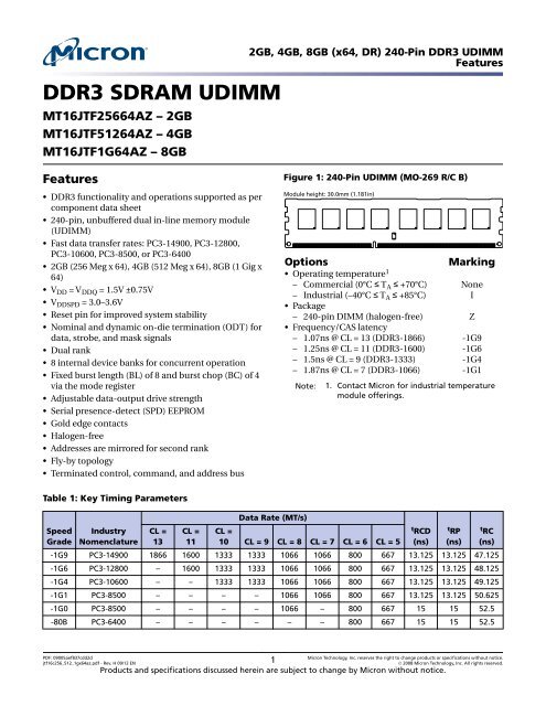
Figure 1: <strong>240</strong>-<strong>Pin</strong> <strong>UDIMM</strong> (MO-269 R/C B)<br />
Module height: 30.0mm (1.181in)<br />
Options Marking<br />
• Operating temperature 1<br />
– Commercial (0°C ≤ T A ≤ +70°C) None<br />
– Industrial (–40°C ≤ T A ≤ +85°C) I<br />
• Package<br />
– <strong>240</strong>-pin DIMM (halogen-free) Z<br />
• Frequency/CAS latency<br />
– 1.07ns @ CL = 13 (D<strong>DR</strong>3-1866) -1G9<br />
– 1.25ns @ CL = 11 (D<strong>DR</strong>3-1600) -1G6<br />
– 1.5ns @ CL = 9 (D<strong>DR</strong>3-1333) -1G4<br />
– 1.87ns @ CL = 7 (D<strong>DR</strong>3-1066) -1G1<br />
Note: 1. Contact <strong>Micron</strong> for industrial temperature<br />
module offerings.<br />
CL =<br />
10 CL = 9 CL = 8 CL = 7 CL = 6 CL = 5<br />
-1G9 PC3-14900 1866 1600 1333 1333 1066 1066 800 667 13.125 13.125 47.125<br />
-1G6 PC3-12800 – 1600 1333 1333 1066 1066 800 667 13.125 13.125 48.125<br />
-1G4 PC3-10600 – – 1333 1333 1066 1066 800 667 13.125 13.125 49.125<br />
-1G1 PC3-8500 – – – – 1066 1066 800 667 13.125 13.125 50.625<br />
-1G0 PC3-8500 – – – – 1066 – 800 667 15 15 52.5<br />
-80B PC3-6400 – – – – – – 800 667 15 15 52.5<br />
PDF: 09005aef837cdd2d<br />
jtf16c256_512_1g<strong>x64</strong>az.pdf - Rev. H 09/12 EN 1 <strong>Micron</strong> Technology, Inc. reserves the right to change products or specifications without notice.<br />
© 2008 <strong>Micron</strong> Technology, Inc. All rights reserved.<br />
Products and specifications discussed herein are subject to change by <strong>Micron</strong> without notice.<br />
t RCD<br />
(ns)<br />
t RP<br />
(ns)<br />
t RC<br />
(ns)
Table 2: Addressing<br />
Parameter <strong>2GB</strong> <strong>4GB</strong> <strong>8GB</strong><br />
Refresh count 8K 8K 8K<br />
Row address 16K A[13:0] 32K A[14:0] 64K A[15:0]<br />
Device bank address 8 BA[2:0] 8 BA[2:0] 8 BA[2:0]<br />
Device page size per bank 1KB 1KB 1KB<br />
Device configuration 1Gb (128 Meg x 8) 2Gb (256 Meg x 8) 4Gb (512 Meg x 8)<br />
Column address 1K A[9:0] 1K A[9:0] 1K A[9:0]<br />
Module rank address 2 S#[1:0] 2 S#[1:0] 2 S#[1:0]<br />
Table 3: Part Numbers and Timing Parameters – <strong>2GB</strong><br />
Base device: MT41J128M8, 1 1Gb D<strong>DR</strong>3 S<strong>DR</strong>AM<br />
Part Number 2<br />
Module<br />
Density Configuration<br />
Module Bandwidth<br />
Memory Clock/ Data<br />
Rate<br />
CL- t RCD- t RP<br />
(Clock Cycles)<br />
MT16JTF25664A(I)Z-1G9__ <strong>2GB</strong> 256 Meg x 64 14.9 GB/s 1.07ns/1866 MT/s 13-13-13<br />
MT16JTF25664A(I)Z-1G6__ <strong>2GB</strong> 256 Meg x 64 12.8 GB/s 1.25ns/1600 MT/s 11-11-11<br />
MT16JTF25664A(I)Z-1G4__ <strong>2GB</strong> 256 Meg x 64 10.6 GB/s 1.5ns/1333 MT/s 9-9-9<br />
MT16JTF25664A(I)Z-1G1__ <strong>2GB</strong> 256 Meg x 64 8.5 GB/s 1.87ns/1066 MT/s 7-7-7<br />
Table 4: Part Numbers and Timing Parameters – <strong>4GB</strong><br />
Base device: MT41J256M8, 1 2Gb D<strong>DR</strong>3 S<strong>DR</strong>AM<br />
Part Number 2<br />
Module<br />
Density Configuration<br />
Module Bandwidth<br />
Memory Clock/ Data<br />
Rate<br />
CL- t RCD- t RP<br />
(Clock Cycles)<br />
MT16JTF51264A(I)Z-1G9__ <strong>4GB</strong> 512 Meg x 64 14.9 GB/s 1.07ns/1866 MT/s 13-13-13<br />
MT16JTF51264A(I)Z-1G6__ <strong>4GB</strong> 512 Meg x 64 12.8 GB/s 1.25ns/1600 MT/s 11-11-11<br />
MT16JTF51264A(I)Z-1G4__ <strong>4GB</strong> 512 Meg x 64 10.6 GB/s 1.5ns/1333 MT/s 9-9-9<br />
MT16JTF51264A(I)Z-1G1__ <strong>4GB</strong> 512 Meg x 64 8.5 GB/s 1.87ns/1066 MT/s 7-7-7<br />
Table 5: Part Numbers and Timing Parameters – <strong>8GB</strong><br />
Base device: MT41J512M8, 1 4Gb D<strong>DR</strong>3 S<strong>DR</strong>AM<br />
Part Number 2<br />
Module<br />
Density Configuration<br />
<strong>2GB</strong>, <strong>4GB</strong>, <strong>8GB</strong> (<strong>x64</strong>, <strong>DR</strong>) <strong>240</strong>-<strong>Pin</strong> D<strong>DR</strong>3 <strong>UDIMM</strong><br />
Features<br />
Module<br />
Bandwidth<br />
Memory Clock/<br />
Data Rate<br />
CL- t RCD- t RP<br />
(Clock Cycles)<br />
MT16JTF1G64A(I)Z-1G9__ <strong>8GB</strong> 1 Gig x 64 14.9 GB/s 1.07ns/1866 MT/s 13-13-13<br />
MT16JTF1G64A(I)Z-1G6__ <strong>8GB</strong> 1 Gig x 64 12.8 GB/s 1.25ns/1600 MT/s 11-11-11<br />
MT16JTF1G64A(I)Z-1G4__ <strong>8GB</strong> 1 Gig x 64 10.6 GB/s 1.5ns/1333 MT/s 9-9-9<br />
MT16JTF1G64A(I)Z-1G1__ <strong>8GB</strong> 1 Gig x 64 8.5 GB/s 1.87ns/1066 MT/s 7-7-7<br />
Notes: 1. Data sheets for the base device parts can be found on <strong>Micron</strong>’s Web site.<br />
2. All part numbers end with a two-place code (not shown), designating component and PCB revisions. Consult<br />
factory for current revision codes. Example: MT16JTF51264AZ-1G6K1.<br />
PDF: 09005aef837cdd2d<br />
jtf16c256_512_1g<strong>x64</strong>az.pdf - Rev. H 09/12 EN 2 <strong>Micron</strong> Technology, Inc. reserves the right to change products or specifications without notice.<br />
© 2008 <strong>Micron</strong> Technology, Inc. All rights reserved.
<strong>Pin</strong> Assignments<br />
Table 6: <strong>Pin</strong> Assignments<br />
<strong>240</strong>-<strong>Pin</strong> <strong>UDIMM</strong> Front <strong>240</strong>-<strong>Pin</strong> <strong>UDIMM</strong> Back<br />
<strong>Pin</strong> Symbol <strong>Pin</strong> Symbol <strong>Pin</strong> Symbol <strong>Pin</strong> Symbol <strong>Pin</strong> Symbol <strong>Pin</strong> Symbol <strong>Pin</strong> Symbol <strong>Pin</strong> Symbol<br />
1 V REFDQ 31 DQ25 61 A2 91 DQ41 121 V SS 151 V SS 181 A1 211 V SS<br />
2 V SS 32 V SS 62 V DD 92 V SS 122 DQ4 152 DM3 182 V DD 212 DM5<br />
3 DQ0 33 DQS3# 63 CK1 93 DQS5# 123 DQ5 153 NC 183 V DD 213 NC<br />
4 DQ1 34 DQS3 64 CK1# 94 DQS5 124 V SS 154 V SS 184 CK0 214 V SS<br />
5 V SS 35 V SS 65 V DD 95 V SS 125 DM0 155 DQ30 185 CK0# 215 DQ46<br />
6 DQS0# 36 DQ26 66 V DD 96 DQ42 126 NC 156 DQ31 186 V DD 216 DQ47<br />
7 DQS0 37 DQ27 67 V REFCA 97 DQ43 127 V SS 157 V SS 187 NC 217 V SS<br />
8 V SS 38 V SS 68 NC 98 V SS 128 DQ6 158 NC 188 A0 218 DQ52<br />
9 DQ2 39 NC 69 V DD 99 DQ48 129 DQ7 159 NC 189 V DD 219 DQ53<br />
10 DQ3 40 NC 70 A10 100 DQ49 130 V SS 160 V SS 190 BA1 220 V SS<br />
11 V SS 41 V SS 71 BA0 101 V SS 131 DQ12 161 NC 191 V DD 221 DM6<br />
12 DQ8 42 NC 72 V DD 102 DQS6# 132 DQ13 162 NC 192 RAS# 222 NC<br />
13 DQ9 43 NC 73 WE# 103 DQS6 133 V SS 163 V SS 193 S0# 223 V SS<br />
14 V SS 44 V SS 74 CAS# 104 V SS 134 DM1 164 NC 194 V DD 224 DQ54<br />
15 DQS1# 45 NC 75 V DD 105 DQ50 135 NC 165 NC 195 ODT0 225 DQ55<br />
16 DQS1 46 NC 76 S1# 106 DQ51 136 V SS 166 V SS 196 A13 226 V SS<br />
17 V SS 47 V SS 77 ODT1 107 V SS 137 DQ14 167 NC 197 V DD 227 DQ60<br />
18 DQ10 48 NC 78 V DD 108 DQ56 138 DQ15 168 RESET# 198 NC 228 DQ61<br />
19 DQ11 49 NC 79 NC 109 DQ57 139 V SS 169 CKE1 199 V SS 229 V SS<br />
20 V SS 50 CKE0 80 V SS 110 V SS 140 DQ20 170 V DD 200 DQ36 230 DM7<br />
21 DQ16 51 V DD 81 DQ32 111 DQS7# 141 DQ21 171 NC/A15 1 201 DQ37 231 NC<br />
22 DQ17 52 BA2 82 DQ33 112 DQS7 142 V SS 172 NC/A14 2 202 V SS 232 V SS<br />
23 V SS 53 NC 83 V SS 113 V SS 143 DM2 173 V DD 203 DM4 233 DQ62<br />
24 DQS2# 54 V DD 84 DQS4# 114 DQ58 144 NC 174 A12 204 NC 234 DQ63<br />
25 DQS2 55 A11 85 DQS4 115 DQ59 145 V SS 175 A9 205 V SS 235 V SS<br />
26 V SS 56 A7 86 V SS 116 V SS 146 DQ22 176 V DD 206 DQ38 236 V DDSPD<br />
27 DQ18 57 V DD 87 DQ34 117 SA0 147 DQ23 177 A8 207 DQ39 237 SA1<br />
28 DQ19 58 A5 88 DQ35 118 SCL 148 V SS 178 A6 208 V SS 238 SDA<br />
29 V SS 59 A4 89 V SS 119 SA2 149 DQ28 179 V DD 209 DQ44 239 V SS<br />
30 DQ24 60 V DD 90 DQ40 120 V TT 150 DQ29 180 A3 210 DQ45 <strong>240</strong> V TT<br />
Notes: 1. <strong>Pin</strong> 171 is NC for <strong>2GB</strong> and <strong>4GB</strong>, A15 for <strong>8GB</strong>.<br />
2. <strong>Pin</strong> 172 is NC for <strong>2GB</strong>, A14 for <strong>4GB</strong> and <strong>8GB</strong>.<br />
<strong>2GB</strong>, <strong>4GB</strong>, <strong>8GB</strong> (<strong>x64</strong>, <strong>DR</strong>) <strong>240</strong>-<strong>Pin</strong> D<strong>DR</strong>3 <strong>UDIMM</strong><br />
<strong>Pin</strong> Assignments<br />
PDF: 09005aef837cdd2d<br />
jtf16c256_512_1g<strong>x64</strong>az.pdf - Rev. H 09/12 EN 3 <strong>Micron</strong> Technology, Inc. reserves the right to change products or specifications without notice.<br />
© 2008 <strong>Micron</strong> Technology, Inc. All rights reserved.
<strong>Pin</strong> Descriptions<br />
Table 7: <strong>Pin</strong> Descriptions<br />
Symbol Type Description<br />
The pin description table below is a comprehensive list of all possible pins for all D<strong>DR</strong>3<br />
modules. All pins listed may not be supported on this module. See <strong>Pin</strong> Assignments for<br />
information specific to this module.<br />
Ax Input Address inputs: Provide the row address for ACTIVE commands, and the column address<br />
and auto precharge bit (A10) for READ/WRITE commands, to select one location<br />
out of the memory array in the respective bank. A10 sampled during a PRECHARGE<br />
command determines whether the PRECHARGE applies to one bank (A10 LOW, bank<br />
selected by BAx) or all banks (A10 HIGH). The address inputs also provide the op-code<br />
during a LOAD MODE command. See the <strong>Pin</strong> Assignments Table for density-specific<br />
addressing information.<br />
BAx Input Bank address inputs: Define the device bank to which an ACTIVE, READ, WRITE, or<br />
PRECHARGE command is being applied. BA define which mode register (MR0, MR1,<br />
MR2, or MR3) is loaded during the LOAD MODE command.<br />
CKx,<br />
CKx#<br />
Input Clock: Differential clock inputs. All control, command, and address input signals are<br />
sampled on the crossing of the positive edge of CK and the negative edge of CK#.<br />
CKEx Input Clock enable: Enables (registered HIGH) and disables (registered LOW) internal circuitry<br />
and clocks on the <strong>DR</strong>AM.<br />
DMx Input Data mask (x8 devices only): DM is an input mask signal for write data. Input data<br />
is masked when DM is sampled HIGH, along with that input data, during a write access.<br />
Although DM pins are input-only, DM loading is designed to match that of the<br />
DQ and DQS pins.<br />
ODTx Input On-die termination: Enables (registered HIGH) and disables (registered LOW) termination<br />
resistance internal to the D<strong>DR</strong>3 S<strong>DR</strong>AM. When enabled in normal operation,<br />
ODT is only applied to the following pins: DQ, DQS, DQS#, DM, and CB. The ODT input<br />
will be ignored if disabled via the LOAD MODE command.<br />
Par_In Input Parity input: Parity bit for Ax, RAS#, CAS#, and WE#.<br />
RAS#, CAS#, WE# Input Command inputs: RAS#, CAS#, and WE# (along with S#) define the command being<br />
entered.<br />
RESET# Input<br />
(LVCMOS)<br />
Reset: RESET# is an active LOW asychronous input that is connected to each <strong>DR</strong>AM<br />
and the registering clock driver. After RESET# goes HIGH, the <strong>DR</strong>AM must be reinitialized<br />
as though a normal power-up was executed.<br />
Sx# Input Chip select: Enables (registered LOW) and disables (registered HIGH) the command<br />
decoder.<br />
SAx Input Serial address inputs: Used to configure the temperature sensor/SPD EEPROM address<br />
range on the I 2 C bus.<br />
SCL Input Serial clock for temperature sensor/SPD EEPROM: Used to synchronize communication<br />
to and from the temperature sensor/SPD EEPROM on the I 2 C bus.<br />
CBx I/O Check bits: Used for system error detection and correction.<br />
DQx I/O Data input/output: Bidirectional data bus.<br />
DQSx,<br />
DQSx#<br />
<strong>2GB</strong>, <strong>4GB</strong>, <strong>8GB</strong> (<strong>x64</strong>, <strong>DR</strong>) <strong>240</strong>-<strong>Pin</strong> D<strong>DR</strong>3 <strong>UDIMM</strong><br />
<strong>Pin</strong> Descriptions<br />
I/O Data strobe: Differential data strobes. Output with read data; edge-aligned with<br />
read data; input with write data; center-aligned with write data.<br />
PDF: 09005aef837cdd2d<br />
jtf16c256_512_1g<strong>x64</strong>az.pdf - Rev. H 09/12 EN 4 <strong>Micron</strong> Technology, Inc. reserves the right to change products or specifications without notice.<br />
© 2008 <strong>Micron</strong> Technology, Inc. All rights reserved.
Table 7: <strong>Pin</strong> Descriptions (Continued)<br />
Symbol Type Description<br />
SDA I/O Serial data: Used to transfer addresses and data into and out of the temperature sensor/SPD<br />
EEPROM on the I 2 C bus.<br />
TDQSx,<br />
TDQSx#<br />
Err_Out# Output<br />
(open drain)<br />
EVENT# Output<br />
(open drain)<br />
Output Redundant data strobe (x8 devices only): TDQS is enabled/disabled via the LOAD<br />
MODE command to the extended mode register (EMR). When TDQS is enabled, DM is<br />
disabled and TDQS and TDQS# provide termination resistance; otherwise, TDQS# are<br />
no function.<br />
Parity error output: Parity error found on the command and address bus.<br />
Temperature event:The EVENT# pin is asserted by the temperature sensor when critical<br />
temperature thresholds have been exceeded.<br />
V DD Supply Power supply: 1.5V ±0.075V. The component V DD and V DDQ are connected to the<br />
module V DD.<br />
V DDSPD Supply Temperature sensor/SPD EEPROM power supply: 3.0–3.6V.<br />
V REFCA Supply Reference voltage: Control, command, and address V DD/2.<br />
V REFDQ Supply Reference voltage: DQ, DM V DD/2.<br />
V SS Supply Ground.<br />
<strong>2GB</strong>, <strong>4GB</strong>, <strong>8GB</strong> (<strong>x64</strong>, <strong>DR</strong>) <strong>240</strong>-<strong>Pin</strong> D<strong>DR</strong>3 <strong>UDIMM</strong><br />
<strong>Pin</strong> Descriptions<br />
V TT Supply Termination voltage: Used for control, command, and address V DD/2.<br />
NC – No connect: These pins are not connected on the module.<br />
NF – No function: These pins are connected within the module, but provide no functionality.<br />
PDF: 09005aef837cdd2d<br />
jtf16c256_512_1g<strong>x64</strong>az.pdf - Rev. H 09/12 EN 5 <strong>Micron</strong> Technology, Inc. reserves the right to change products or specifications without notice.<br />
© 2008 <strong>Micron</strong> Technology, Inc. All rights reserved.
DQ Map<br />
Table 8: Component-to-Module DQ Map<br />
Component<br />
Reference<br />
Number<br />
Component<br />
DQ Module DQ<br />
Module <strong>Pin</strong><br />
Number<br />
<strong>2GB</strong>, <strong>4GB</strong>, <strong>8GB</strong> (<strong>x64</strong>, <strong>DR</strong>) <strong>240</strong>-<strong>Pin</strong> D<strong>DR</strong>3 <strong>UDIMM</strong><br />
DQ Map<br />
Component<br />
Reference<br />
Number<br />
Component<br />
DQ Module DQ<br />
Module <strong>Pin</strong><br />
Number<br />
U1 0 2 9 U2 0 10 18<br />
1 5 123 1 13 132<br />
2 7 129 2 15 138<br />
3 1 4 3 9 13<br />
4 6 128 4 14 137<br />
5 4 122 5 12 131<br />
6 3 10 6 11 19<br />
7 0 3 7 8 12<br />
U3 0 18 27 U4 0 26 36<br />
1 21 141 1 29 150<br />
2 23 147 2 31 156<br />
3 17 22 3 25 31<br />
4 22 146 4 30 155<br />
5 20 140 5 28 149<br />
6 19 28 6 27 37<br />
7 16 21 7 24 30<br />
U5 0 34 87 U6 0 42 96<br />
1 37 201 1 45 210<br />
2 39 207 2 47 216<br />
3 33 82 3 41 91<br />
4 38 206 4 46 215<br />
5 36 200 5 44 209<br />
6 35 88 6 43 97<br />
7 32 81 7 40 90<br />
U7 0 50 105 U8 0 58 114<br />
1 53 219 1 61 228<br />
2 55 225 2 63 234<br />
3 49 100 3 57 109<br />
4 54 224 4 62 233<br />
5 52 218 5 60 227<br />
6 51 106 6 59 115<br />
7 48 99 7 56 108<br />
PDF: 09005aef837cdd2d<br />
jtf16c256_512_1g<strong>x64</strong>az.pdf - Rev. H 09/12 EN 6 <strong>Micron</strong> Technology, Inc. reserves the right to change products or specifications without notice.<br />
© 2008 <strong>Micron</strong> Technology, Inc. All rights reserved.
Table 8: Component-to-Module DQ Map (Continued)<br />
Component<br />
Reference<br />
Number<br />
Component<br />
DQ Module DQ<br />
Module <strong>Pin</strong><br />
Number<br />
<strong>2GB</strong>, <strong>4GB</strong>, <strong>8GB</strong> (<strong>x64</strong>, <strong>DR</strong>) <strong>240</strong>-<strong>Pin</strong> D<strong>DR</strong>3 <strong>UDIMM</strong><br />
DQ Map<br />
Component<br />
Reference<br />
Number<br />
Component<br />
DQ Module DQ<br />
Module <strong>Pin</strong><br />
Number<br />
U10 0 61 228 U11 0 53 219<br />
1 58 114 1 50 105<br />
2 57 109 2 49 100<br />
3 63 234 3 55 225<br />
4 56 108 4 48 99<br />
5 59 115 5 51 106<br />
6 60 227 6 52 218<br />
7 62 233 7 54 224<br />
U12 0 45 210 U13 0 37 201<br />
1 42 96 1 34 87<br />
2 41 91 2 33 82<br />
3 47 216 3 39 207<br />
4 40 90 4 32 81<br />
5 43 97 5 35 88<br />
6 44 209 6 36 200<br />
7 46 215 7 38 206<br />
U14 0 29 150 U15 0 21 141<br />
1 26 36 1 18 27<br />
2 25 31 2 17 22<br />
3 31 156 3 23 147<br />
4 24 30 4 16 21<br />
5 27 37 5 19 28<br />
6 28 149 6 20 140<br />
7 30 155 7 22 146<br />
U16 0 13 132 U17 0 5 123<br />
1 10 18 1 2 9<br />
2 9 13 2 1 4<br />
3 15 138 3 7 129<br />
4 8 12 4 0 3<br />
5 11 19 5 3 10<br />
6 12 131 6 4 122<br />
7 14 137 7 6 128<br />
PDF: 09005aef837cdd2d<br />
jtf16c256_512_1g<strong>x64</strong>az.pdf - Rev. H 09/12 EN 7 <strong>Micron</strong> Technology, Inc. reserves the right to change products or specifications without notice.<br />
© 2008 <strong>Micron</strong> Technology, Inc. All rights reserved.
S1#<br />
S0#<br />
DQS0#<br />
DQS0<br />
DM0<br />
Functional Block Diagram<br />
Figure 2: Functional Block Diagram<br />
DQS1#<br />
DQS1<br />
DM1<br />
DQ0<br />
DQ1<br />
DQ2<br />
DQ3<br />
DQ4<br />
DQ5<br />
DQ6<br />
DQ7<br />
DQ8<br />
DQ9<br />
DQ10<br />
DQ11<br />
DQ12<br />
DQ13<br />
DQ14<br />
DQ15<br />
DQS2#<br />
DQS2<br />
DM2<br />
DQ16<br />
DQ17<br />
DQ18<br />
DQ19<br />
DQ20<br />
DQ21<br />
DQ22<br />
DQ23<br />
DQS3#<br />
DQS3<br />
DM3<br />
V SS<br />
V SS<br />
V SS<br />
DQ24<br />
DQ25<br />
DQ26<br />
DQ27<br />
DQ28<br />
DQ29<br />
DQ30<br />
DQ31<br />
V SS<br />
DQ<br />
DQ<br />
DQ<br />
DQ<br />
DQ<br />
DQ<br />
DQ<br />
DQ<br />
ZQ<br />
DQ<br />
DQ<br />
DQ<br />
DQ<br />
DQ<br />
DQ<br />
DQ<br />
DQ<br />
ZQ<br />
DQ<br />
DQ<br />
DQ<br />
DQ<br />
DQ<br />
DQ<br />
DQ<br />
DQ<br />
ZQ<br />
DQ<br />
DQ<br />
DQ<br />
DQ<br />
DQ<br />
DQ<br />
DQ<br />
DQ<br />
ZQ<br />
DM CS# DQS DQS#<br />
U1<br />
DM CS# DQS DQS#<br />
U2<br />
DM CS# DQS DQS#<br />
U3<br />
DM CS# DQS DQS#<br />
U4<br />
DQ<br />
DQ<br />
DQ<br />
DQ<br />
DQ<br />
DQ<br />
DQ<br />
DQ<br />
DQ<br />
DQ<br />
DQ<br />
DQ<br />
DQ<br />
DQ<br />
DQ<br />
DQ<br />
DQ<br />
DQ<br />
DQ<br />
DQ<br />
DQ<br />
DQ<br />
DQ<br />
DQ<br />
DQ<br />
DQ<br />
DQ<br />
DQ<br />
DQ<br />
DQ<br />
DQ<br />
DQ<br />
DM CS# DQS DQS# DM CS# DQS DQS# DM CS# DQS DQS#<br />
U17<br />
DM CS# DQS DQS#<br />
U16<br />
DM CS# DQS DQS#<br />
U15<br />
DM CS# DQS DQS#<br />
U14<br />
ZQ<br />
ZQ<br />
ZQ<br />
ZQ<br />
V SS<br />
V SS<br />
V SS<br />
V SS<br />
DQS4#<br />
DQS4<br />
DM4<br />
DQS5#<br />
DQS5<br />
DM5<br />
DQS6#<br />
DQS6<br />
DM6<br />
DQS7#<br />
DQS7<br />
DM7<br />
DQ32<br />
DQ33<br />
DQ34<br />
DQ35<br />
DQ36<br />
DQ37<br />
DQ38<br />
DQ39<br />
V SS<br />
DQ40<br />
DQ41<br />
DQ42<br />
DQ43<br />
DQ44<br />
DQ45<br />
DQ46<br />
DQ47<br />
DQ48<br />
DQ49<br />
DQ50<br />
DQ51<br />
DQ52<br />
DQ53<br />
DQ54<br />
DQ55<br />
DQ56<br />
DQ57<br />
DQ58<br />
DQ59<br />
DQ60<br />
DQ61<br />
DQ62<br />
DQ63<br />
V SS<br />
V SS<br />
V SS<br />
<strong>2GB</strong>, <strong>4GB</strong>, <strong>8GB</strong> (<strong>x64</strong>, <strong>DR</strong>) <strong>240</strong>-<strong>Pin</strong> D<strong>DR</strong>3 <strong>UDIMM</strong><br />
Functional Block Diagram<br />
DQ<br />
DQ<br />
DQ<br />
DQ<br />
DQ<br />
DQ<br />
DQ<br />
DQ<br />
ZQ<br />
DQ<br />
DQ<br />
DQ<br />
DQ<br />
DQ<br />
DQ<br />
DQ<br />
DQ<br />
ZQ<br />
DQ<br />
DQ<br />
DQ<br />
DQ<br />
DQ<br />
DQ<br />
DQ<br />
DQ<br />
ZQ<br />
DQ<br />
DQ<br />
DQ<br />
DQ<br />
DQ<br />
DQ<br />
DQ<br />
DQ<br />
ZQ<br />
U5<br />
U6<br />
DQ<br />
DQ<br />
DQ<br />
DQ<br />
DQ<br />
DQ<br />
DQ<br />
DQ<br />
DQ<br />
DQ<br />
DQ<br />
DQ<br />
DQ<br />
DQ<br />
DQ<br />
DQ<br />
U13<br />
DM CS# DQS DQS# DM CS# DQS DQS#<br />
U7<br />
DQ<br />
DQ<br />
DQ<br />
DQ<br />
DQ<br />
DQ<br />
DQ<br />
DQ<br />
U12<br />
DM CS# DQS DQS# DM CS# DQS DQS#<br />
U8<br />
DQ<br />
DQ<br />
DQ<br />
DQ<br />
DQ<br />
DQ<br />
DQ<br />
DQ<br />
U11<br />
DM CS# DQS DQS# DM CS# DQ S DQS#<br />
U10<br />
ZQ<br />
ZQ<br />
ZQ<br />
ZQ<br />
V SS<br />
BA[2:0]<br />
A[15/14:0]<br />
RAS#<br />
CAS#<br />
WE#<br />
CKE0<br />
CKE1<br />
ODT0<br />
ODT1<br />
RESET#<br />
CKE[1:0], A[15/14:0],<br />
RAS#, CAS#, WE#,<br />
S#[1:0], ODT[1:0], BA[2:0]<br />
V SS<br />
V SS<br />
V SS<br />
CK[1:0]<br />
CK#[1:0]<br />
V DDSPD<br />
V DD<br />
V TT<br />
V REFCA<br />
V REFDQ<br />
V SS<br />
SCL<br />
CK0<br />
CK0#<br />
CK1<br />
CK1#<br />
BA[2:0]: D<strong>DR</strong>3 S<strong>DR</strong>AM<br />
A[15/14/13:0]: D<strong>DR</strong>3 S<strong>DR</strong>AM<br />
RAS#: D<strong>DR</strong>3 S<strong>DR</strong>AM<br />
CAS#: D<strong>DR</strong>3 S<strong>DR</strong>AM<br />
WE#: D<strong>DR</strong>3 S<strong>DR</strong>AM<br />
CKE0: Rank 0<br />
CKE1: Rank 1<br />
ODT0: Rank 0<br />
ODT1: Rank 1<br />
RESET#: D<strong>DR</strong>3 S<strong>DR</strong>AM<br />
Command, address, and clock line terminations<br />
D<strong>DR</strong>3<br />
S<strong>DR</strong>AM<br />
D<strong>DR</strong>3<br />
S<strong>DR</strong>AM<br />
U9<br />
SPD EEPROM<br />
WP A0 A1 A2<br />
VSS SA0 SA1 SA2<br />
Rank 0 = U1–U8<br />
Rank 1 = U10–U17<br />
Rank 0<br />
Rank 1<br />
SDA<br />
V TT<br />
SPD EEPROM<br />
V DD<br />
D<strong>DR</strong>3 S<strong>DR</strong>AM<br />
Address, command,<br />
and control termination<br />
D<strong>DR</strong>3 S<strong>DR</strong>AM<br />
D<strong>DR</strong>3 S<strong>DR</strong>AM<br />
D<strong>DR</strong>3 S<strong>DR</strong>AM<br />
Note: 1. The ZQ ball on each D<strong>DR</strong>3 component is connected to an external <strong>240</strong>Ω resistor that is<br />
tied to ground. Used for the calibration of the component’s on-die termination and output<br />
driver.<br />
PDF: 09005aef837cdd2d<br />
jtf16c256_512_1g<strong>x64</strong>az.pdf - Rev. H 09/12 EN 8 <strong>Micron</strong> Technology, Inc. reserves the right to change products or specifications without notice.<br />
© 2008 <strong>Micron</strong> Technology, Inc. All rights reserved.
General Description<br />
Fly-By Topology<br />
D<strong>DR</strong>3 S<strong>DR</strong>AM modules are high-speed, CMOS dynamic random access memory modules<br />
that use internally configured 8-bank D<strong>DR</strong>3 S<strong>DR</strong>AM devices. D<strong>DR</strong>3 S<strong>DR</strong>AM modules<br />
use D<strong>DR</strong> architecture to achieve high-speed operation. D<strong>DR</strong>3 architecture is essentially<br />
an 8n-prefetch architecture with an interface designed to transfer two data words<br />
per clock cycle at the I/O pins. A single read or write access for the D<strong>DR</strong>3 S<strong>DR</strong>AM module<br />
effectively consists of a single 8n-bit-wide, one-clock-cycle data transfer at the internal<br />
<strong>DR</strong>AM core and eight corresponding n-bit-wide, one-half-clock-cycle data transfers<br />
at the I/O pins.<br />
D<strong>DR</strong>3 modules use two sets of differential signals: DQS, DQS# to capture data and CK<br />
and CK# to capture commands, addresses, and control signals. Differential clocks and<br />
data strobes ensure exceptional noise immunity for these signals and provide precise<br />
crossing points to capture input signals.<br />
D<strong>DR</strong>3 modules use faster clock speeds than earlier D<strong>DR</strong> technologies, making signal<br />
quality more important than ever. For improved signal quality, the clock, control, command,<br />
and address buses have been routed in a fly-by topology, where each clock, control,<br />
command, and address pin on each <strong>DR</strong>AM is connected to a single trace and terminated<br />
(rather than a tree structure, where the termination is off the module near the<br />
connector). Inherent to fly-by topology, the timing skew between the clock and DQS signals<br />
can be easily accounted for by using the write-leveling feature of D<strong>DR</strong>3.<br />
Serial Presence-Detect EEPROM Operation<br />
<strong>2GB</strong>, <strong>4GB</strong>, <strong>8GB</strong> (<strong>x64</strong>, <strong>DR</strong>) <strong>240</strong>-<strong>Pin</strong> D<strong>DR</strong>3 <strong>UDIMM</strong><br />
General Description<br />
D<strong>DR</strong>3 S<strong>DR</strong>AM modules incorporate serial presence-detect. The SPD data is stored in a<br />
256-byte EEPROM. The first 128 bytes are programmed by <strong>Micron</strong> to comply with<br />
JEDEC standard JC-45, "Appendix X: Serial Presence Detect (SPD) for D<strong>DR</strong>3 S<strong>DR</strong>AM<br />
Modules." These bytes identify module-specific timing parameters, configuration information,<br />
and physical attributes. The remaining 128 bytes of storage are available for use<br />
by the customer. System READ/WRITE operations between the master (system logic)<br />
and the slave EEPROM device occur via a standard I 2 C bus using the DIMM’s SCL<br />
(clock) SDA (data), and SA (address) pins. Write protect (WP) is connected to V SS, permanently<br />
disabling hardware write protection. For further information refer to <strong>Micron</strong><br />
technical note TN-04-42, "Memory Module Serial Presence-Detect."<br />
PDF: 09005aef837cdd2d<br />
jtf16c256_512_1g<strong>x64</strong>az.pdf - Rev. H 09/12 EN 9 <strong>Micron</strong> Technology, Inc. reserves the right to change products or specifications without notice.<br />
© 2008 <strong>Micron</strong> Technology, Inc. All rights reserved.
Electrical Specifications<br />
Table 9: Absolute Maximum Ratings<br />
Stresses greater than those listed may cause permanent damage to the module. This is a<br />
stress rating only, and functional operation of the module at these or any other conditions<br />
outside those indicated in each device's data sheet is not implied. Exposure to absolute<br />
maximum rating conditions for extended periods may adversely affect reliability.<br />
Symbol Parameter Min Max Units<br />
V DD V DD supply voltage relative to V SS –0.4 1.975 V<br />
V IN, V OUT Voltage on any pin relative to V SS –0.4 1.975 V<br />
Table 10: Operating Conditions<br />
Symbol Parameter Min Nom Max Units Notes<br />
V DD V DD supply voltage 1.425 1.5 1.575 V<br />
I VTT Termination reference current from V TT –600 – 600 mA<br />
V TT<br />
I I<br />
I OZ<br />
Termination reference voltage – command address<br />
bus<br />
Input leakage current;<br />
Any input 0V ≤ V IN ≤ V DD;<br />
V REF input 0V ≤ V IN ≤ 0.95V<br />
(All other pins not under test = 0V)<br />
Output leakage current;<br />
0V ≤ V OUT ≤ V DDQ; DQs and ODT are<br />
disabled<br />
Address inputs<br />
RAS#, CAS#,<br />
WE#, BA<br />
S#, CKE, ODT,<br />
CK, CK#<br />
0.483 x V DD 0.5 x V DD 0.517 x V DD V 1<br />
–32 0 32 µA<br />
–16 0 16<br />
DM –4 0 4<br />
DQ, DQS, DQS# –10 0 10 µA<br />
I VREF V REF leakage current; V REF = valid V REF level –16 0 16 µA<br />
T A<br />
T C<br />
Module ambient operating temperature<br />
D<strong>DR</strong>3 S<strong>DR</strong>AM component case operating<br />
temperature<br />
<strong>2GB</strong>, <strong>4GB</strong>, <strong>8GB</strong> (<strong>x64</strong>, <strong>DR</strong>) <strong>240</strong>-<strong>Pin</strong> D<strong>DR</strong>3 <strong>UDIMM</strong><br />
Electrical Specifications<br />
Commercial 0 – 70 °C 2, 3<br />
Industrial –40 – 85 °C<br />
Commercial 0 – 95 °C 2, 3, 4<br />
Industrial –40 – 95 °C<br />
Notes: 1. V TT termination voltage in excess of the stated limit will adversely affect the command<br />
and address signals’ voltage margin and will reduce timing margins.<br />
2. T A and T C are simultaneous requirements.<br />
3. For further information, refer to technical note TN-00-08: ”Thermal Applications,”<br />
available on <strong>Micron</strong>’s Web site.<br />
4. The refresh rate is required to double when 85°C < T C ≤ 95°C.<br />
PDF: 09005aef837cdd2d<br />
jtf16c256_512_1g<strong>x64</strong>az.pdf - Rev. H 09/12 EN 10 <strong>Micron</strong> Technology, Inc. reserves the right to change products or specifications without notice.<br />
© 2008 <strong>Micron</strong> Technology, Inc. All rights reserved.
<strong>DR</strong>AM Operating Conditions<br />
Recommended AC operating conditions are given in the D<strong>DR</strong>3 component data sheets.<br />
Component specifications are available on <strong>Micron</strong>’s Web site. Module speed grades correlate<br />
with component speed grades, as shown below.<br />
Table 11: Module and Component Speed Grades<br />
D<strong>DR</strong>3 components may exceed the listed module speed grades; module may not be available in all listed speed grades<br />
Design Considerations<br />
Module Speed Grade Component Speed Grade<br />
-2G1 -093<br />
-1G9 -107<br />
-1G6 -125<br />
-1G4 -15E<br />
-1G1 -187E<br />
-1G0 -187<br />
-80C -25E<br />
-80B -25<br />
Simulations<br />
<strong>Micron</strong> memory modules are designed to optimize signal integrity through carefully designed<br />
terminations, controlled board impedances, routing topologies, trace length<br />
matching, and decoupling. However, good signal integrity starts at the system level.<br />
<strong>Micron</strong> encourages designers to simulate the signal characteristics of the system's<br />
memory bus to ensure adequate signal integrity of the entire memory system.<br />
Power<br />
<strong>2GB</strong>, <strong>4GB</strong>, <strong>8GB</strong> (<strong>x64</strong>, <strong>DR</strong>) <strong>240</strong>-<strong>Pin</strong> D<strong>DR</strong>3 <strong>UDIMM</strong><br />
<strong>DR</strong>AM Operating Conditions<br />
Operating voltages are specified at the <strong>DR</strong>AM, not at the edge connector of the module.<br />
Designers must account for any system voltage drops at anticipated power levels to ensure<br />
the required supply voltage is maintained.<br />
PDF: 09005aef837cdd2d<br />
jtf16c256_512_1g<strong>x64</strong>az.pdf - Rev. H 09/12 EN 11 <strong>Micron</strong> Technology, Inc. reserves the right to change products or specifications without notice.<br />
© 2008 <strong>Micron</strong> Technology, Inc. All rights reserved.
I DD Specifications<br />
Table 12: D<strong>DR</strong>3 I DD Specifications and Conditions – <strong>2GB</strong> (Die Revision G)<br />
<strong>2GB</strong>, <strong>4GB</strong>, <strong>8GB</strong> (<strong>x64</strong>, <strong>DR</strong>) <strong>240</strong>-<strong>Pin</strong> D<strong>DR</strong>3 <strong>UDIMM</strong><br />
I DD Specifications<br />
Values are for the MT41J128M8 D<strong>DR</strong>3 S<strong>DR</strong>AM only and are computed from values specified in the 1Gb (128 Meg x 8) component<br />
data sheet<br />
Parameter Symbol 1866 1600 1333 1066 Units<br />
Operating current 0: One bank ACTIVATE-to-PRECHARGE I DD0 1 656 656 616 576 mA<br />
Operating current 1: One bank ACTIVATE-to-READ-to-PRECHARGE I DD1 1 816 816 776 736 mA<br />
Precharge power-down current: Slow exit I DD2P0 2 192 192 192 192 mA<br />
Precharge power-down current: Fast exit I DD2P1 2 560 480 480 400 mA<br />
Precharge quiet standby current I DD2Q 2 720 640 560 560 mA<br />
Precharge standby current I DD2N 2 800 720 640 560 mA<br />
Precharge standby ODT current I DD2NT 2 576 536 496 456 mA<br />
Active power-down current I DD3P 2 560 560 480 480 mA<br />
Active standby current I DD3N 2 800 720 640 640 mA<br />
Burst read operating current I DD4R 1 1336 1216 1096 936 mA<br />
Burst write operating current I DD4W 1 1376 1256 1096 976 mA<br />
Refresh current I DD5B 1 1496 1456 1416 1376 mA<br />
Self refresh temperature current: MAX T C = 85°C I DD6 2 128 128 128 128 mA<br />
Self refresh temperature current (SRT-enabled): MAX T C = 95°C I DD6ET 2 160 160 160 160 mA<br />
All banks interleaved read current I DD7 1 2160 2056 1976 1656 mA<br />
Reset current I DD8 2 224 224 224 224 mA<br />
Notes: 1. One module rank in the active I DD; the other rank in I DD2P0 (slow exit).<br />
2. All ranks in this I DD condition.<br />
PDF: 09005aef837cdd2d<br />
jtf16c256_512_1g<strong>x64</strong>az.pdf - Rev. H 09/12 EN 12 <strong>Micron</strong> Technology, Inc. reserves the right to change products or specifications without notice.<br />
© 2008 <strong>Micron</strong> Technology, Inc. All rights reserved.
Table 13: D<strong>DR</strong>3 I DD Specifications and Conditions – <strong>4GB</strong> (Die Revision M)<br />
<strong>2GB</strong>, <strong>4GB</strong>, <strong>8GB</strong> (<strong>x64</strong>, <strong>DR</strong>) <strong>240</strong>-<strong>Pin</strong> D<strong>DR</strong>3 <strong>UDIMM</strong><br />
I DD Specifications<br />
Values are for the MT41J256M8 D<strong>DR</strong>3 S<strong>DR</strong>AM only and are computed from values specified in the 2Gb (256 Meg x 8) component<br />
data sheet<br />
Parameter Symbol 1866 1600 1333 1066 Units<br />
Operating current 0: One bank ACTIVATE-to-PRECHARGE I DD0 1 696 656 616 576 mA<br />
Operating current 1: One bank ACTIVATE-to-READ-to-PRECHARGE I DD1 1 776 736 696 656 mA<br />
Precharge power-down current: Slow exit I DD2P0 2 192 192 192 192 mA<br />
Precharge power-down current: Fast exit I DD2P1 2 672 592 512 432 mA<br />
Precharge quiet standby current I DD2Q 2 720 640 560 480 mA<br />
Precharge standby current I DD2N 2 768 688 608 528 mA<br />
Precharge standby ODT current I DD2NT 2 496 456 416 376 mA<br />
Active power-down current I DD3P 2 880 800 720 640 mA<br />
Active standby current I DD3N 2 960 880 800 720 mA<br />
Burst read operating current I DD4R 1 1464 1344 1224 1136 mA<br />
Burst write operating current I DD4W 1 1376 1256 1136 1016 mA<br />
Refresh current I DD5B 1 1696 1656 1616 1576 mA<br />
Self refresh temperature current: MAX T C = 85°C I DD6 2 192 192 192 192 mA<br />
Self refresh temperature current (SRT-enabled): MAX T C = 95°C I DD6ET 2 216 216 216 216 mA<br />
All banks interleaved read current I DD7 1 2136 2016 1896 1776 mA<br />
Reset current I DD8 2 208 208 208 208 mA<br />
Notes: 1. One module rank in the active I DD; the other rank in I DD2P0 (slow exit).<br />
2. All ranks in this I DD condition.<br />
PDF: 09005aef837cdd2d<br />
jtf16c256_512_1g<strong>x64</strong>az.pdf - Rev. H 09/12 EN 13 <strong>Micron</strong> Technology, Inc. reserves the right to change products or specifications without notice.<br />
© 2008 <strong>Micron</strong> Technology, Inc. All rights reserved.
Table 14: D<strong>DR</strong>3 I DD Specifications and Conditions – <strong>4GB</strong> (Die Revision K)<br />
<strong>2GB</strong>, <strong>4GB</strong>, <strong>8GB</strong> (<strong>x64</strong>, <strong>DR</strong>) <strong>240</strong>-<strong>Pin</strong> D<strong>DR</strong>3 <strong>UDIMM</strong><br />
I DD Specifications<br />
Values are for the MT41J256M8 D<strong>DR</strong>3 S<strong>DR</strong>AM only and are computed from values specified in the 2Gb (256 Meg x 8) component<br />
data sheet<br />
Parameter Symbol 1866 1600 1333 1066 Units<br />
Operating current 0: One bank ACTIVATE-to-PRECHARGE I DD0 1 440 432 424 408 mA<br />
Operating current 1: One bank ACTIVATE-to-READ-to-PRECHARGE I DD1 1 560 544 528 496 mA<br />
Precharge power-down current: Slow exit I DD2P0 2 192 192 192 192 mA<br />
Precharge power-down current: Fast exit I DD2P1 2 <strong>240</strong> <strong>240</strong> <strong>240</strong> <strong>240</strong> mA<br />
Precharge quiet standby current I DD2Q 2 352 352 352 352 mA<br />
Precharge standby current I DD2N 2 368 368 368 368 mA<br />
Precharge standby ODT current I DD2NT 2 384 368 352 328 mA<br />
Active power-down current I DD3P 2 352 352 352 352 mA<br />
Active standby current I DD3N 2 592 560 528 496 mA<br />
Burst read operating current I DD4R 1 976 896 800 696 mA<br />
Burst write operating current I DD4W 1 1008 920 824 728 mA<br />
Refresh current I DD5B 1 1008 992 984 968 mA<br />
Self refresh temperature current: MAX T C = 85°C I DD6 2 192 192 192 192 mA<br />
Self refresh temperature current (SRT-enabled): MAX T C = 95°C I DD6ET 2 216 216 216 216 mA<br />
All banks interleaved read current I DD7 1 1464 1400 1352 1120 mA<br />
Reset current I DD8 2 208 208 208 208 mA<br />
Notes: 1. One module rank in the active I DD; the other rank in I DD2P0 (slow exit).<br />
2. All ranks in this I DD condition.<br />
PDF: 09005aef837cdd2d<br />
jtf16c256_512_1g<strong>x64</strong>az.pdf - Rev. H 09/12 EN 14 <strong>Micron</strong> Technology, Inc. reserves the right to change products or specifications without notice.<br />
© 2008 <strong>Micron</strong> Technology, Inc. All rights reserved.
Table 15: D<strong>DR</strong>3 I DD Specifications and Conditions – <strong>8GB</strong> (Die Revision D)<br />
<strong>2GB</strong>, <strong>4GB</strong>, <strong>8GB</strong> (<strong>x64</strong>, <strong>DR</strong>) <strong>240</strong>-<strong>Pin</strong> D<strong>DR</strong>3 <strong>UDIMM</strong><br />
I DD Specifications<br />
Values are for the MT41J512M8 D<strong>DR</strong>3 S<strong>DR</strong>AM only and are computed from values specified in the 4Gb (512 Meg x 8) component<br />
data sheet<br />
Parameter Symbol 1866 1600 1333 1066 Units<br />
Operating current 0: One bank ACTIVATE-to-PRECHARGE I DD0 1 840 760 680 640 mA<br />
Operating current 1: One bank ACTIVATE-to-READ-to-PRECHARGE I DD1 1 896 856 816 776 mA<br />
Precharge power-down current: Slow exit I DD2P0 2 320 320 320 320 mA<br />
Precharge power-down current: Fast exit I DD2P1 2 672 592 512 480 mA<br />
Precharge quiet standby current I DD2Q 2 832 752 672 624 mA<br />
Precharge standby current I DD2N 2 880 800 720 672 mA<br />
Precharge standby ODT current I DD2NT 2 600 560 520 480 mA<br />
Active power-down current I DD3P 2 1088 1008 928 848 mA<br />
Active standby current I DD3N 2 1072 992 912 832 mA<br />
Burst read operating current I DD4R 1 1816 1656 1496 1336 mA<br />
Burst write operating current I DD4W 1 1640 1480 1320 1160 mA<br />
Refresh current I DD5B 1 2000 1920 1840 1800 mA<br />
Self refresh temperature current: MAX T C = 85°C I DD6 2 352 352 352 352 mA<br />
Self refresh temperature current (SRT-enabled): MAX T C = 95°C I DD6ET 2 448 448 448 448 mA<br />
All banks interleaved read current I DD7 1 2800 2480 2160 1840 mA<br />
Reset current I DD8 2 352 352 352 352 mA<br />
Notes: 1. One module rank in the active I DD; the other rank in I DD2P0 (slow exit).<br />
2. All ranks in this I DD condition.<br />
PDF: 09005aef837cdd2d<br />
jtf16c256_512_1g<strong>x64</strong>az.pdf - Rev. H 09/12 EN 15 <strong>Micron</strong> Technology, Inc. reserves the right to change products or specifications without notice.<br />
© 2008 <strong>Micron</strong> Technology, Inc. All rights reserved.
<strong>2GB</strong>, <strong>4GB</strong>, <strong>8GB</strong> (<strong>x64</strong>, <strong>DR</strong>) <strong>240</strong>-<strong>Pin</strong> D<strong>DR</strong>3 <strong>UDIMM</strong><br />
I DD Specifications<br />
Table 16: D<strong>DR</strong>3 I DD Specifications and Conditions – <strong>8GB</strong> (Die Revisions E and J)<br />
Values are for the MT41J512M8 D<strong>DR</strong>3 S<strong>DR</strong>AM only and are computed from values specified in the 4Gb (512 Meg x 8) component<br />
data sheet<br />
Parameter Symbol 1866 1600 1333 1066 Units<br />
Operating current 0: One bank ACTIVATE-to-PRECHARGE I DD0 1 640 584 520 496 mA<br />
Operating current 1: One bank ACTIVATE-to-READ-to-PRECHARGE I DD1 1 704 672 540 616 mA<br />
Precharge power-down current: Slow exit I DD2P0 2 288 288 288 288 mA<br />
Precharge power-down current: Fast exit I DD2P1 2 592 512 448 416 mA<br />
Precharge quiet standby current I DD2Q 2 560 512 448 416 mA<br />
Precharge standby current I DD2N 2 560 512 464 448 mA<br />
Precharge standby ODT current I DD2NT 2 480 456 424 400 mA<br />
Active power-down current I DD3P 2 656 608 560 512 mA<br />
Active standby current I DD3N 2 656 608 560 512 mA<br />
Burst read operating current I DD4R 1 1536 1400 1264 1128 mA<br />
Burst write operating current I DD4W 1 1272 1144 1024 904 mA<br />
Refresh current I DD5B 1 1440 1384 1328 1296 mA<br />
Self refresh temperature current: MAX T C = 85°C I DD6 2 320 320 320 320 mA<br />
Self refresh temperature current (SRT-enabled): MAX T C = 95°C I DD6ET 2 400 400 400 400 mA<br />
All banks interleaved read current I DD7 1 2152 1904 1664 1424 mA<br />
Reset current I DD8 2 320 320 320 320 mA<br />
Notes: 1. One module rank in the active I DD; the other rank in I DD2P0 (slow exit).<br />
2. All ranks in this I DD condition.<br />
PDF: 09005aef837cdd2d<br />
jtf16c256_512_1g<strong>x64</strong>az.pdf - Rev. H 09/12 EN 16 <strong>Micron</strong> Technology, Inc. reserves the right to change products or specifications without notice.<br />
© 2008 <strong>Micron</strong> Technology, Inc. All rights reserved.
Serial Presence-Detect EEPROM<br />
For the latest SPD data, refer to <strong>Micron</strong>'s SPD page: www.micron.com/SPD.<br />
Table 17: Serial Presence-Detect EEPROM DC Operating Conditions<br />
All voltages referenced to V DDSPD<br />
Parameter/Condition Symbol Min Max Units<br />
Supply voltage V DDSPD 3.0 3.6 V<br />
Input low voltage: Logic 0; All inputs V IL –0.6 V DDSPD + 0.3 V<br />
Input high voltage: Logic 1; All inputs V IH V DDSPD + 0.7 V DDSPD + 1.0 V<br />
Output low voltage: I OUT = 3mA V OL – 0.4 V<br />
Input leakage current: V IN = GND to V DD I LI 0.1 2.0 µA<br />
Output leakage current: V OUT = GND to V DD I LO 0.05 2.0 µA<br />
Table 18: Serial Presence-Detect EEPROM AC Operating Conditions<br />
Parameter/Condition Symbol Min Max Units Notes<br />
Clock frequency t SCL 10 400 kHz<br />
Clock pulse width HIGH time t HIGH 0.6 – µs<br />
Clock pulse width LOW time t LOW 1.3 – µs<br />
SDA rise time t R – 300 µs 1<br />
SDA fall time t F 20 300 ns 1<br />
Data-in setup time t SU:DAT 100 – ns<br />
Data-in hold time t HD:DI 0 – µs<br />
Data-out hold time t HD:DAT 200 900 ns<br />
Data out access time from SCL LOW t AA:DAT 0.2 0.9 µs 2<br />
Start condition setup time t SU:STA 0.6 – µs 3<br />
Start condition hold time t HD:STA 0.6 – µs<br />
Stop condition setup time t SU:STO 0.6 – µs<br />
Time the bus must be free before a new transition can<br />
start<br />
<strong>2GB</strong>, <strong>4GB</strong>, <strong>8GB</strong> (<strong>x64</strong>, <strong>DR</strong>) <strong>240</strong>-<strong>Pin</strong> D<strong>DR</strong>3 <strong>UDIMM</strong><br />
Serial Presence-Detect EEPROM<br />
t BUF 1.3 – µs<br />
WRITE time t W – 10 ms<br />
Notes: 1. Guaranteed by design and characterization, not necessarily tested.<br />
2. To avoid spurious start and stop conditions, a minimum delay is placed between the falling<br />
edge of SCL and the falling or rising edge of SDA.<br />
3. For a restart condition, or following a WRITE cycle.<br />
PDF: 09005aef837cdd2d<br />
jtf16c256_512_1g<strong>x64</strong>az.pdf - Rev. H 09/12 EN 17 <strong>Micron</strong> Technology, Inc. reserves the right to change products or specifications without notice.<br />
© 2008 <strong>Micron</strong> Technology, Inc. All rights reserved.
Module Dimensions<br />
Figure 3: <strong>240</strong>-<strong>Pin</strong> D<strong>DR</strong>3 <strong>UDIMM</strong><br />
0.9 (0.035) TYP<br />
0.50 (0.02) R<br />
(4X)<br />
0.75 (0.03) R<br />
(8X)<br />
2.50 (0.098) D<br />
(2X)<br />
2.30 (0.091) TYP<br />
2.20 (0.087) TYP<br />
1.45 (0.057) TYP<br />
5.1 (0.2) TYP<br />
3.05 (0.12) TYP<br />
<strong>Pin</strong> 1<br />
U1 U2 U3 U4<br />
15.0 (0.59)<br />
4X TYP<br />
54.68 (2.15)<br />
TYP<br />
Front view<br />
133.50 (5.256)<br />
133.20 (5.244)<br />
0.76 (0.030) R<br />
123.0 (4.84)<br />
TYP<br />
1.0 (0.039)<br />
TYP<br />
0.80 (0.031)<br />
TYP<br />
<strong>Pin</strong> <strong>240</strong> <strong>Pin</strong> 121<br />
5.0 (0.197) TYP<br />
71.0 (2.79)<br />
TYP<br />
U9<br />
Back view<br />
U5 U6 U7 U8<br />
1.0 (0.039) R (8X)<br />
U10 U11 U12 U13 U14 U15 U16 U17<br />
<strong>2GB</strong>, <strong>4GB</strong>, <strong>8GB</strong> (<strong>x64</strong>, <strong>DR</strong>) <strong>240</strong>-<strong>Pin</strong> D<strong>DR</strong>3 <strong>UDIMM</strong><br />
Module Dimensions<br />
47.0 (1.85)<br />
TYP<br />
9.5 (0.374)<br />
TYP<br />
17.3 (0.68)<br />
TYP<br />
<strong>Pin</strong> 120<br />
45°, 4X<br />
3.1 (0.122) 2X TYP<br />
3.0 (0.118) 4X TYP<br />
23.3 (0.92)<br />
TYP<br />
30.50 (1.20)<br />
29.85 (1.175)<br />
4.0 (0.157)<br />
MAX<br />
1.37 (0.054)<br />
1.17 (0.046)<br />
Notes: 1. All dimensions are in millimeters (inches); MAX/MIN or typical (TYP) where noted.<br />
2. The dimensional diagram is for reference only. Refer to the JEDEC MO document for additional<br />
design dimensions.<br />
8000 S. Federal Way, P.O. Box 6, Boise, ID 83707-0006, Tel: 208-368-3900<br />
www.micron.com/productsupport Customer Comment Line: 800-932-4992<br />
<strong>Micron</strong> and the <strong>Micron</strong> logo are trademarks of <strong>Micron</strong> Technology, Inc.<br />
All other trademarks are the property of their respective owners.<br />
This data sheet contains minimum and maximum limits specified over the power supply and temperature range set forth herein.<br />
Although considered final, these specifications are subject to change, as further product development and data characterization sometimes<br />
occur.<br />
PDF: 09005aef837cdd2d<br />
jtf16c256_512_1g<strong>x64</strong>az.pdf - Rev. H 09/12 EN 18 <strong>Micron</strong> Technology, Inc. reserves the right to change products or specifications without notice.<br />
© 2008 <strong>Micron</strong> Technology, Inc. All rights reserved.


