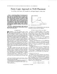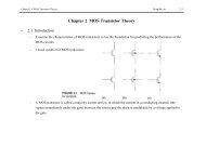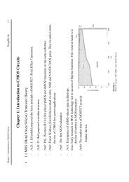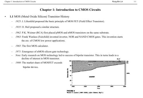
Chapter 1: Introduction to CMOS Circuits
Chapter 1: Introduction to CMOS Circuits
Chapter 1: Introduction to CMOS Circuits

Create successful ePaper yourself
Turn your PDF publications into a flip-book with our unique Google optimized e-Paper software.
<strong>Chapter</strong> 1: <strong>Introduction</strong> <strong>to</strong> <strong>CMOS</strong> <strong>Circuits</strong> Rung-Bin Lin1-9• 1.5.2 Combinational Logic:– If two N-SWITCHES (or P-SWITCHES) are placed in series, this structure yields an “AND” function.– If two N-SWITCHES (or P-SWITCHES) are placed in parallel, this structure yields an “OR” function.– By using combinations of these structures, <strong>CMOS</strong> combinational gates can be constructed.
<strong>Chapter</strong> 1: <strong>Introduction</strong> <strong>to</strong> <strong>CMOS</strong> <strong>Circuits</strong> Rung-Bin Lin1-10• 1.5.3 The NAND Gate: F = A•B (derive the NAND function from schematics)– Using the structures in Fig. 1.5(a) and Fig. 1.5(d)
<strong>Chapter</strong> 1: <strong>Introduction</strong> <strong>to</strong> <strong>CMOS</strong> <strong>Circuits</strong> Rung-Bin Lin1-11– Pull-down truth table– Pull-up truth table– NAND gate truth table
<strong>Chapter</strong> 1: <strong>Introduction</strong> <strong>to</strong> <strong>CMOS</strong> <strong>Circuits</strong> Rung-Bin Lin1-12• 1.5.4 The NOR Gate: F = ( A + B) (Synthesize the NOR structure from NOR function)– NOR gate Karnaugh Map and truth table– From pull-down truth table, this suggests that the structure in Fig. 1.5(c) be used for N-SWITHCES array.From pull-up truth table, this suggests the structure in Fig. 1.5(b) be used for P-SWITHCES array.Note that1 the outputs of these are fully res<strong>to</strong>red <strong>to</strong> “1”or “0” for any input combinations since there isalways a path from V DDor V SSsupplies <strong>to</strong> theoutput and the full supply voltages appear at theoutputs. This considerably simplifies the circuitdesign.2 the output is never at crowbarred statebecause there is never a path from the VDD <strong>to</strong>the VSS supplies for any input combination.
<strong>Chapter</strong> 1: <strong>Introduction</strong> <strong>to</strong> <strong>CMOS</strong> <strong>Circuits</strong> Rung-Bin Lin1-13• 1.5.5 Compound Gates:– A compound gate is formed by using a combination of seriesand parallel-switch structures.– For example : <strong>to</strong> constructF• For n-side (pull-down),= (( A•B)+ ( C • D))(1)take the expression (( A • B)+ ( C • D)).(2) From A• B by using the structure in Fig. 1.5(a).(3) Form C • D by using the structure in Fig. 1.5(a).(4) Treat the structures obtained in (2) and (3) as twosimple switches and then use the structure in Fig.1.5(c) <strong>to</strong> form ( A • B)+ ( C • D).• For p-side (pull-up),(1) Convert the expression (( A • B)+ ( C • D))in<strong>to</strong> sumof-product( A + B)• ( C + D)and disregard the “bar”on each input variable, we obtain the expression( A + B)• ( C + D.)(2) Form ( A + B) by using the structure in Fig. 1.5(c).(3) Form ( C + D) by using the structure in Fig. 1.5(c).(4) Treat the structures obtained in (2) and (3) as twosimpleswitches and then use the structure in Fig. 1.5(b) <strong>to</strong>form ( A + B)• ( C + D).
<strong>Chapter</strong> 1: <strong>Introduction</strong> <strong>to</strong> <strong>CMOS</strong> <strong>Circuits</strong> Rung-Bin Lin1-14– Yet another example for F= ( A + B + C)• D– Implementation of 4 input AND gateF= A•B • C • D = A • B • C • D = A + B + C + D = A • B • C • D
<strong>Chapter</strong> 1: <strong>Introduction</strong> <strong>to</strong> <strong>CMOS</strong> <strong>Circuits</strong> Rung-Bin Lin1-15• 1.5.6 Multiplexers :– Complementary switches can be used <strong>to</strong> select between a number of inputs, thus forming a multiplexerfunction.– 2-input <strong>CMOS</strong> multiplexer: Output = A • S + B • S
<strong>Chapter</strong> 1: <strong>Introduction</strong> <strong>to</strong> <strong>CMOS</strong> <strong>Circuits</strong> Rung-Bin Lin1-16• 1.5.7 Memory-Latches and Registers– Level sensitive latch : data input is passed <strong>to</strong> the output during the moment that clock is active. (for example,clock is high)• Inputs: D and CLK.• Outputs: Q and -Q.• when CLK=1, Q is set <strong>to</strong> D and -Q is set <strong>to</strong> -D.• When CLK=0, Q and -Q do not change even the input D would change.
<strong>Chapter</strong> 1: <strong>Introduction</strong> <strong>to</strong> <strong>CMOS</strong> <strong>Circuits</strong> Rung-Bin Lin1-17– edge-triggered register: data is transmitted only when clock is changing its state.• By combining two level-sensitive latches, one positive sensitive (called slave) and one negative sensitive(called master) as shown in the following figure.
<strong>Chapter</strong> 1: <strong>Introduction</strong> <strong>to</strong> <strong>CMOS</strong> <strong>Circuits</strong> Rung-Bin Lin1-18• 1.6 Circuit and System Representations– To facilitate the designing of complex digital systems, a specific set of abstractions have been developed <strong>to</strong>describe integrated electronic systems.
<strong>Chapter</strong> 1: <strong>Introduction</strong> <strong>to</strong> <strong>CMOS</strong> <strong>Circuits</strong> Rung-Bin Lin1-19– Three distinct domains:• Behavioral domain specifies what a system does.• Structural domain specifies how entities are connected <strong>to</strong>gether <strong>to</strong> effect the prescribed behavior.• Physical domain specifies how <strong>to</strong> actually build a structure that has the required connectivity <strong>to</strong>implement the prescribed behavior.– Each design domain may be specified at a variety of levels of abstraction.– Six levels of abstraction:• Architectural level,• Algorithmic level,• Module or functional block level,• Logical level,• Switch level, and• Circuit level.– Which domain and what level of abstraction can be used for a design?Ans.: A design is expressed in terms of the three design domains, while the levels of abstraction that areused depends on design style and circuit complexity.
<strong>Chapter</strong> 1: <strong>Introduction</strong> <strong>to</strong> <strong>CMOS</strong> <strong>Circuits</strong> Rung-Bin Lin1-20• 1.6.1 Behavioral Representation– A behavioral representation describes how a particular design should respond <strong>to</strong> a given set of inputs.– Behavior may be specified by Boolean equations, tables of input and output values or algorithms.– Behavior can be implemented by• Standard high level languages such as the C language, etc.• Hardware description language such as VHDL, Verilog, etc.– Example: An n-bit adder by cascading n 1-bit adders1-bit adder: A and B are two operand inputs and C is carry input; S is a sum output and CO is a carryoutput. The behavior of 1-bit adder can be represented by• Boolean functions:S = A • B • C + A • B • C + A • B • C + A • B • CCO = A • B + A • C + B • C• Truth table
<strong>Chapter</strong> 1: <strong>Introduction</strong> <strong>to</strong> <strong>CMOS</strong> <strong>Circuits</strong> Rung-Bin Lin1-21• A verilog module• A primitive• A verilog module with gate delay
<strong>Chapter</strong> 1: <strong>Introduction</strong> <strong>to</strong> <strong>CMOS</strong> <strong>Circuits</strong> Rung-Bin Lin1-22• 1.6.2 Structural Representation– A structural specification specifies how components are connected <strong>to</strong> perform a certain function (behavior).– 4-bit adder by connecting 4 1-bit modules (components):– 1-bit adder consisting of sum and carry modules:
<strong>Chapter</strong> 1: <strong>Introduction</strong> <strong>to</strong> <strong>CMOS</strong> <strong>Circuits</strong> Rung-Bin Lin1-23– Carry module consisting of logic gates:– Carry module consisting of MOS transis<strong>to</strong>r:
<strong>Chapter</strong> 1: <strong>Introduction</strong> <strong>to</strong> <strong>CMOS</strong> <strong>Circuits</strong> Rung-Bin Lin1-24– A structural view of a 4-bit <strong>CMOS</strong> adder. – Circuit level representation for assessing the timingbehavior of a logic gate by SPICE:
<strong>Chapter</strong> 1: <strong>Introduction</strong> <strong>to</strong> <strong>CMOS</strong> <strong>Circuits</strong> Rung-Bin Lin1-25• 1.6.3 Physical Representation– The physical specification for a circuit is used <strong>to</strong> define how a particular part has <strong>to</strong> be constructed <strong>to</strong> create aspecific structure and hence yield the prescribed behavior.– Physical layout for the 4-bit adder at module level.• Written in HDL • Represented by A picture
<strong>Chapter</strong> 1: <strong>Introduction</strong> <strong>to</strong> <strong>CMOS</strong> <strong>Circuits</strong> Rung-Bin Lin1-26– Physical layout for the 1-bit adder at transis<strong>to</strong>r level.• Written in GDSII (a kind of graphical language)• Represented by polygons
<strong>Chapter</strong> 1: <strong>Introduction</strong> <strong>to</strong> <strong>CMOS</strong> <strong>Circuits</strong> Rung-Bin Lin1-27• 1.7 An Example: Triangular waveform genera<strong>to</strong>r• 1.7.1 Specification– 4-bit precision– Use an 8-bit DIP package– Less than 10 milliwatts power dissipation– Signal description:• RST: Reset input• CLK: 1MHZ clock input• VDD: 5V power supply• VSS: Ground• WAVE: 4-bit output• System level diagram
<strong>Chapter</strong> 1: <strong>Introduction</strong> <strong>to</strong> <strong>CMOS</strong> <strong>Circuits</strong> Rung-Bin Lin1-28• 1.7.2 Behavioral Description– C subroutine– Verilog module
<strong>Chapter</strong> 1: <strong>Introduction</strong> <strong>to</strong> <strong>CMOS</strong> <strong>Circuits</strong> Rung-Bin Lin1-29• 1.7.3 Structural Description:– Can be obtained by au<strong>to</strong>matic <strong>to</strong>ols that can convert a behavioral description in<strong>to</strong> a structural one.– A structural description for the whole system which consists of 8 I/O pads and a module called triangle-gen.– A structural description of triangle-gen.
<strong>Chapter</strong> 1: <strong>Introduction</strong> <strong>to</strong> <strong>CMOS</strong> <strong>Circuits</strong> Rung-Bin Lin1-30– A structural description of inc-dec.– A structural description of inc-dec-bit.
<strong>Chapter</strong> 1: <strong>Introduction</strong> <strong>to</strong> <strong>CMOS</strong> <strong>Circuits</strong> Rung-Bin Lin1-31– A conventional schematic diagram for triangle genera<strong>to</strong>r.
<strong>Chapter</strong> 1: <strong>Introduction</strong> <strong>to</strong> <strong>CMOS</strong> <strong>Circuits</strong> Rung-Bin Lin1-32– A hierarchy diagram of the whole chip.• The cells at the bot<strong>to</strong>m of the hierarchy tree are called leaf cells. There is a corresponding physicaldescription for every leaf cell.
<strong>Chapter</strong> 1: <strong>Introduction</strong> <strong>to</strong> <strong>CMOS</strong> <strong>Circuits</strong> Rung-Bin Lin1-33• 1.7.4 Physical Description– All modules except leaf cells in a hierarchy tree can be transformed in<strong>to</strong> modules that consist of only leaf cells.Thus a hierarchical design can be transformed in<strong>to</strong> a (flat) design which consist of only leaf cells.– A physical layout of a design is a physical description that specifies the positions of leaf cells (called cellplacement) and the routes of all connections among connections (called net routing).– Standard cell: A kind of leaf cells usuallywith the same height and varying width.– A symbolic representation of the chip layout.
<strong>Chapter</strong> 1: <strong>Introduction</strong> <strong>to</strong> <strong>CMOS</strong> <strong>Circuits</strong> Rung-Bin Lin1-34• 1.7.5 Summary– The majority of chip design is and must be highly au<strong>to</strong>mated <strong>to</strong> improve productivity.– The overall design flow.
<strong>Chapter</strong> 1: <strong>Introduction</strong> <strong>to</strong> <strong>CMOS</strong> <strong>Circuits</strong> Rung-Bin Lin1-35• 1.8 <strong>CMOS</strong> Scorecard– Variety of Technology• GaAs: fastest raw gate speed.• Bipolar: speed next <strong>to</strong> GaAS (Gallium Arsenide).• Advanced <strong>CMOS</strong>: speed close behind Bipolar.• <strong>CMOS</strong>: highest density and lowest power.– Main attributes of <strong>CMOS</strong>• Fully res<strong>to</strong>red logic levels.• Rise and fall times are of the same order.• Dense and low power memory.• Transmission gates pass both logic levels well.• Power supply varies from 1.5 <strong>to</strong> 15 volts.• Precharging characteristics- Both n_type and p_type devices are available for pre charging a bus <strong>to</strong> V DD and V SS .• Require 2n devices for an n-input gate.• Regular layout.• 1.9 Summary– MOS his<strong>to</strong>ry– MOS transis<strong>to</strong>r Switches– <strong>CMOS</strong> Logic– Circuit and System Representations