Chapter 1: Introduction to CMOS Circuits
Chapter 1: Introduction to CMOS Circuits
Chapter 1: Introduction to CMOS Circuits

Create successful ePaper yourself
Turn your PDF publications into a flip-book with our unique Google optimized e-Paper software.
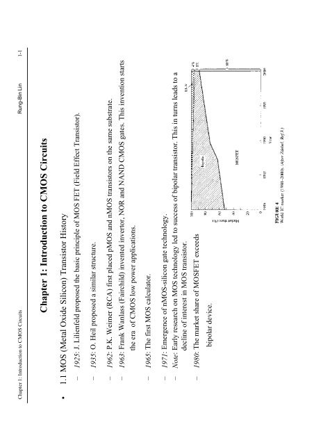
<strong>Chapter</strong> 1: <strong>Introduction</strong> <strong>to</strong> <strong>CMOS</strong> <strong>Circuits</strong> Rung-Bin Lin1-1<strong>Chapter</strong> 1: <strong>Introduction</strong> <strong>to</strong> <strong>CMOS</strong> <strong>Circuits</strong>• 1.1 MOS (Metal Oxide Silicon) Transis<strong>to</strong>r His<strong>to</strong>ry– 1925: J. Lilienfeld proposed the basic principle of MOS FET (Field Effect Transis<strong>to</strong>r).– 1935: O. Heil proposed a similar structure.– 1962: P.K. Weimer (RCA) first placed pMOS and nMOS transis<strong>to</strong>rs on the same substrate.– 1963: Frank Wanlass (Fairchild) invented inver<strong>to</strong>r, NOR and NAND <strong>CMOS</strong> gates. This invention startsthe era of <strong>CMOS</strong> low power applications.– 1965: The first MOS calcula<strong>to</strong>r.– 1971: Emergence of nMOS-silicon gate technology.– Note: Early research on MOS technology led <strong>to</strong> success of bipolar transis<strong>to</strong>r. This in turns leads <strong>to</strong> adecline of interest in MOS transis<strong>to</strong>r.– 1980: The market share of MOSFET exceedsbipolar device.
<strong>Chapter</strong> 1: <strong>Introduction</strong> <strong>to</strong> <strong>CMOS</strong> <strong>Circuits</strong> Rung-Bin Lin1-2• 1.3 MOS Transis<strong>to</strong>r– Basic starting material: Single crystal of siliconformed as wafers (4-inch, 6-inch, 8-inch, 12-inch).– MOS structure is created by superposing severallayers of conducting, insulating, and transis<strong>to</strong>rformingmaterials <strong>to</strong> create a sandwich-likestructure by way of a series of chemicalprocessing steps such as:• oxidation of the silicon, diffusion ofimpurities in<strong>to</strong> silicon <strong>to</strong> give it certainconduction characteristics, and• deposition and etching of aluminum onsilicon <strong>to</strong> form interconnection.– Two types of transis<strong>to</strong>rs (Figure 1.1):• nMOS: with negatively diffused (doped)source and drain on lightly p-dopedsubstrate.• pMOS: with positively diffused source anddrain on lightly n-doped substrate.
<strong>Chapter</strong> 1: <strong>Introduction</strong> <strong>to</strong> <strong>CMOS</strong> <strong>Circuits</strong> Rung-Bin Lin1-3– Four terminals of a transis<strong>to</strong>r:• Gate: usually formed by polycrystalline silicon (polysilicon for short). It is a control input thataffects the flow of electrical current between source and drain.• Source and Drain: Formed by diffusion. They are physically equivalent and the name assignmentdepends on the direction of current flow.• Substrate: the fourth terminal of MOS transis<strong>to</strong>r and will be discussed later.– Note that p-type transis<strong>to</strong>r (pMOS) has n-doped substrate and n-type transis<strong>to</strong>r (nMOS) has p-dopedsubstrate.
<strong>Chapter</strong> 1: <strong>Introduction</strong> <strong>to</strong> <strong>CMOS</strong> <strong>Circuits</strong> Rung-Bin Lin1-4• 1.4 MOS Transis<strong>to</strong>r Switches– The gate controls the flow of current between source the and the drain. This allows us <strong>to</strong> treat the MOStransis<strong>to</strong>rs as simple on/off switches.– Logic value system:• 1: Between 1.5 and 15 volts• z: High Impedance (a circuits node not connecting <strong>to</strong> either Power or Ground)• 0: Zero volts– Strength of the “1” and “0” signals:• Strength of a signal is measured by its ability <strong>to</strong> sink or source current.• Power (PWR, V DD): Strongest 1.• Ground (GND, V SS): Strongest 0.• By convention, current is sourced from Power, and Ground sinks current.• nMOS switch (N-SWITCH) is closed or ON if the drain and the source are connected . This occurswhen there is a “1” on the gate .– Pass a good 0.– Pass a poor 1.• nMOS switch (N-SWITCH) is closed or ON when there is a “0” on the gate.– Pass a good 1.– Pass a poor 0.
<strong>Chapter</strong> 1: <strong>Introduction</strong> <strong>to</strong> <strong>CMOS</strong> <strong>Circuits</strong> Rung-Bin Lin1-5
<strong>Chapter</strong> 1: <strong>Introduction</strong> <strong>to</strong> <strong>CMOS</strong> <strong>Circuits</strong> Rung-Bin Lin1-7• 1.5 <strong>CMOS</strong> Logic• 1.5.1 Inverter :– Truth Table :– “ Input 0 Æ Output 1” suggests a P-SWITCH connected from a “1” source (V DD) <strong>to</strong> the output.– “ Input 1 Æ Output 0” suggests an N-SWITCH connected from a “0” source <strong>to</strong> the output.– Inverter Circuit
<strong>Chapter</strong> 1: <strong>Introduction</strong> <strong>to</strong> <strong>CMOS</strong> <strong>Circuits</strong> Rung-Bin Lin1-8• Fully complementary <strong>CMOS</strong> gate always has an N-SWITCH array (pull-down) <strong>to</strong> connect theoutput <strong>to</strong> “0” (V SS ) and a P-SWITCH array (pull-up) <strong>to</strong> connect the output <strong>to</strong> “1” (V DD )1nP-SWITCHESOUT1nN-SWITCHES– With independent inputs, the output logic level of a <strong>CMOS</strong> gate can be in any of the following four states:....¯¯¯¯¯¯¯¯
<strong>Chapter</strong> 1: <strong>Introduction</strong> <strong>to</strong> <strong>CMOS</strong> <strong>Circuits</strong> Rung-Bin Lin1-9• 1.5.2 Combinational Logic:– If two N-SWITCHES (or P-SWITCHES) are placed in series, this structure yields an “AND” function.– If two N-SWITCHES (or P-SWITCHES) are placed in parallel, this structure yields an “OR” function.– By using combinations of these structures, <strong>CMOS</strong> combinational gate can be constructed.• 1.5.3 The NAND Gate: F = A • B (derive the NAND function from schematics)– Using the structures in Fig. 1.5(a) and Fig. 1.5(d)
<strong>Chapter</strong> 1: <strong>Introduction</strong> <strong>to</strong> <strong>CMOS</strong> <strong>Circuits</strong> Rung-Bin Lin1-10– Pull-down truth table– Pull-up truth table– NAND gate truth table
<strong>Chapter</strong> 1: <strong>Introduction</strong> <strong>to</strong> <strong>CMOS</strong> <strong>Circuits</strong> Rung-Bin Lin1-11• 1.5.4 The NOR Gate: F = ( A + B) (Synthesize the NOR structure from NOR function)– NOR gate Karnaugh Map and truth table– From pull-down truth table, this suggests that the structure in Fig. 1.5(c) be used for N-SWITHCES array.From pull-up truth table, this suggests the structure in Fig. 1.5(b) be used for P-SWITHCES array.Note thatM the outputs of these are fully res<strong>to</strong>red <strong>to</strong>“1” or “0” for any input combinations sincethere is always a path from V DDor V SSsupplies <strong>to</strong> the output and the full supplyvoltages appear at the outputs. Thisconsiderably simplifies the circuit design.N the output is never at crowbarred statebecause there is never a path from the VDD<strong>to</strong> the VSS supplies for any inputcombination.
<strong>Chapter</strong> 1: <strong>Introduction</strong> <strong>to</strong> <strong>CMOS</strong> <strong>Circuits</strong> Rung-Bin Lin1-13– Yet another example for F = ( A + B + C ) • D– Implementation of 4 input AND gateF = A • B • C • D = A • B • C • D = A + B + C + D = A • B • C • D
<strong>Chapter</strong> 1: <strong>Introduction</strong> <strong>to</strong> <strong>CMOS</strong> <strong>Circuits</strong> Rung-Bin Lin1-14• 1.5.6 Multiplexers :– Complementary switches can be used <strong>to</strong> select between a number of inputs, thus forming a multiplexerfunction.– 2-input <strong>CMOS</strong> multiplexer: Output = A • S + B • S
<strong>Chapter</strong> 1: <strong>Introduction</strong> <strong>to</strong> <strong>CMOS</strong> <strong>Circuits</strong> Rung-Bin Lin1-15• 1.5.7 Memory-Latches and Registers– Level sensitive latch : data input is passed <strong>to</strong> the output during the moment that clock is active. (forexample, clock is high)• Inputs: D and CLK.• Outputs: Q and -Q.• when CLK=1, Q is set <strong>to</strong> D and -Q is set <strong>to</strong> -D.• When CLK=0, Q and -Q do not change even the input D would change.
<strong>Chapter</strong> 1: <strong>Introduction</strong> <strong>to</strong> <strong>CMOS</strong> <strong>Circuits</strong> Rung-Bin Lin1-16– edge-triggered register: data is transmitted only when clock is changing its state.• By combining two level-sensitive latches, one positive sensitive (called master) and one negativesensitive (called slave) as shown in the following figure.
<strong>Chapter</strong> 1: <strong>Introduction</strong> <strong>to</strong> <strong>CMOS</strong> <strong>Circuits</strong> Rung-Bin Lin1-17• 1.6 Circuit and System Representations– To facilitate the designing of complex digital systems, a specific set of abstractions have been developed<strong>to</strong> describe integrated electronic systems.
<strong>Chapter</strong> 1: <strong>Introduction</strong> <strong>to</strong> <strong>CMOS</strong> <strong>Circuits</strong> Rung-Bin Lin1-18– Three distinct domains:• Behavioral domain specifies what a system does.• Structural domain specifies how entities are connected <strong>to</strong>gether <strong>to</strong> effect the prescribed behavior.• Physical domain specifies how <strong>to</strong> actually build a structure that has the required connectivity <strong>to</strong>implement the prescribed behavior.– Each design domain may be specified at a variety of levels of abstraction.– Six levels of abstraction:• Architectural level,• Algorithmic level,• Module or functional block level,• Logical level,• Switch level, and• Circuit level.– Which domain and what level of abstraction can be used for a design?Ans.: A design is expressed in terms of the three design domains, while the levels of abstraction that areused depends on design style and circuit complexity.
<strong>Chapter</strong> 1: <strong>Introduction</strong> <strong>to</strong> <strong>CMOS</strong> <strong>Circuits</strong> Rung-Bin Lin1-20• A verilog module• A primitive• A verilog module with gate delay
<strong>Chapter</strong> 1: <strong>Introduction</strong> <strong>to</strong> <strong>CMOS</strong> <strong>Circuits</strong> Rung-Bin Lin1-21• 1.6.2 Structural Representation– A structural specification specifies how components are connected <strong>to</strong> perform a certain function(behavior).– 4-bit adder by connecting 4 1-bit modules (components):– 1-bit adder consisting of sum and carry modules:
<strong>Chapter</strong> 1: <strong>Introduction</strong> <strong>to</strong> <strong>CMOS</strong> <strong>Circuits</strong> Rung-Bin Lin1-22– Carry module consisting of logic gates:– Carry module consisting of MOS transis<strong>to</strong>r:
<strong>Chapter</strong> 1: <strong>Introduction</strong> <strong>to</strong> <strong>CMOS</strong> <strong>Circuits</strong> Rung-Bin Lin1-23– A structural view of a 4-bit <strong>CMOS</strong> adder. – Circuit level representation for assessing the timingbehavior of a logic gate by SPICE:
<strong>Chapter</strong> 1: <strong>Introduction</strong> <strong>to</strong> <strong>CMOS</strong> <strong>Circuits</strong> Rung-Bin Lin1-24• 1.6.3 Physical Representation– The physical specification for a circuit is used <strong>to</strong> define how a particular part has <strong>to</strong> be constructed <strong>to</strong>create a specific structure and hence yield the prescribed behavior.– Physical layout for the 4-bit adder at module level.• Written in HDL • Represented by A picture
<strong>Chapter</strong> 1: <strong>Introduction</strong> <strong>to</strong> <strong>CMOS</strong> <strong>Circuits</strong> Rung-Bin Lin1-25– Physical layout for the 1-bit adder at transis<strong>to</strong>r level.• Written in GDSII (a kind of graphical language)• Represented by polygons
<strong>Chapter</strong> 1: <strong>Introduction</strong> <strong>to</strong> <strong>CMOS</strong> <strong>Circuits</strong> Rung-Bin Lin1-26• 1.7 An Example: Triangular waveform genera<strong>to</strong>r• 1.7.1 Specification:– 4-bit precision– Use an 8-bit DIP package– Less than 10 milliwatts power dissipation– Signal description:• RST: Reset input• CLK: 1MHZ clock input• VDD: 5V power supply• VSS: Ground• WAVE: 4-bit output• System level diagram
<strong>Chapter</strong> 1: <strong>Introduction</strong> <strong>to</strong> <strong>CMOS</strong> <strong>Circuits</strong> Rung-Bin Lin1-27• 1.7.2 Behavioral Description:– C subroutine– Verilog module
<strong>Chapter</strong> 1: <strong>Introduction</strong> <strong>to</strong> <strong>CMOS</strong> <strong>Circuits</strong> Rung-Bin Lin1-28• 1.7.3 Structural Description:– Can be obtained by au<strong>to</strong>matic <strong>to</strong>ols that can convert a behavioral description in<strong>to</strong> a structural one.– A structural description for the whole system which consists of 8 I/O pads and a module called triangle-gen.– A structural description of triangle-gen.
<strong>Chapter</strong> 1: <strong>Introduction</strong> <strong>to</strong> <strong>CMOS</strong> <strong>Circuits</strong> Rung-Bin Lin1-29– A structural description of inc-dec.– A structural description of inc-dec-bit.
<strong>Chapter</strong> 1: <strong>Introduction</strong> <strong>to</strong> <strong>CMOS</strong> <strong>Circuits</strong> Rung-Bin Lin1-30– A conventional schematic diagram for triangle genera<strong>to</strong>r.
<strong>Chapter</strong> 1: <strong>Introduction</strong> <strong>to</strong> <strong>CMOS</strong> <strong>Circuits</strong> Rung-Bin Lin1-31– A hierarchy diagram of the whole chip.• The cells at the bot<strong>to</strong>m of the hierarchy tree are called leaf cells. There is a corresponding physicaldescription for every leaf cell.
<strong>Chapter</strong> 1: <strong>Introduction</strong> <strong>to</strong> <strong>CMOS</strong> <strong>Circuits</strong> Rung-Bin Lin1-32• 1.7.4 Physical Description– All modules except leaf cells in a hierarchy tree can be transformed in<strong>to</strong> modules that consist of only leafcells. Thus a hierarchical design can be transformed in<strong>to</strong> a (flat) design which consist of only leaf cells.– A physical layout of a design is a physical description that specifies the positions of leaf cells (called cellplacement) and the routes of all connections among connections (called net routing).– Standard cell: A kind of leaf cells usuallywith the same height and varying width.– A symbolic representation of the chip layout.
<strong>Chapter</strong> 1: <strong>Introduction</strong> <strong>to</strong> <strong>CMOS</strong> <strong>Circuits</strong> Rung-Bin Lin1-33• 1.7.5 Summary– The majority of chip design is and must be highly au<strong>to</strong>mated <strong>to</strong> improve productivity.– The overall design flow.
<strong>Chapter</strong> 1: <strong>Introduction</strong> <strong>to</strong> <strong>CMOS</strong> <strong>Circuits</strong> Rung-Bin Lin1-34• 1.8 <strong>CMOS</strong> Scorecard– Variety of Technology• GaAs: fastest raw gate speed.• Bipolar: speed next <strong>to</strong> GAS.• Advanced <strong>CMOS</strong>: speed close behind Bipolar.• <strong>CMOS</strong>: highest density and lowest power.– Main attributes of <strong>CMOS</strong>• Fully res<strong>to</strong>red logic levels.• Rise and fall times are of the same order.• Dense and low power memory.• Transmission gates pass both logic levels well.• Power supply varies from 1.5 <strong>to</strong> 15 volts.• Precharging characteristics- Both n_type and p_type devices are available for pre charging a bus <strong>to</strong>V DDand V SS.• Require 2n devices for an n-input gate.• Regular layout.• 1.9 Summary– MOS his<strong>to</strong>ry– MOS transis<strong>to</strong>r Switches– <strong>CMOS</strong> Logic– Circuit and System Representations