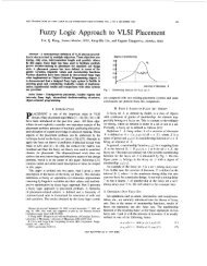
A clocking technique for FPGA pipelined designs
A clocking technique for FPGA pipelined designs
A clocking technique for FPGA pipelined designs

You also want an ePaper? Increase the reach of your titles
YUMPU automatically turns print PDFs into web optimized ePapers that Google loves.
688 O. Cadenas, G. Megson / Journal of Systems Architecture 50 (2004) 687–696datapath control, is an example of a simple elasticpipeline. Keeping the processing throughput inelastic pipelines requires extra control in synchronouspipelines, and is often application-specific.For instance, designing a FIFO. Sutherland in hisclassical work [16] inspires a persistent interest inasynchronous pipelining motivated by its originalsimplicity and regularity <strong>for</strong> implementing elasticpipelining.<strong>FPGA</strong>s do not have the key elements used bytoday’s asynchronous <strong>designs</strong> since they are orientatedto implement circuits synchronously [6]. Indeed,asynchronous elements are costly toimplement in <strong>FPGA</strong>s. For example, a Muller C-element, the most frequently used element <strong>for</strong>controlling micropipelining, takes 1 CLB (Xilinxconfigurable logic block). Consequently, special<strong>FPGA</strong> architectures <strong>for</strong> asynchronous design havebeen proposed, see [5] <strong>for</strong> example. More pragmaticef<strong>for</strong>ts have concentrated on optimizing asynchronouselements commonly at the CMOS level [15].We introduce, in Section 3, a new <strong>clocking</strong><strong>technique</strong> referred to as PP-pipelining, that betterexploits commercial <strong>FPGA</strong> resources <strong>for</strong> asynchronous-likecomputation. PP-pipelines use simpleedge-triggered D-type flip-flops as registers andso suitable <strong>for</strong> efficient <strong>FPGA</strong> implementation. APP-pipeline has a synchronous control mechanismrun by a global clock to generate local clock signalsin the <strong>for</strong>m of pulses and hence the registersdo not share a global clock. The basic controlmechanism is built on a simple state machineaccepting asynchronous status signals fromneighboring stages. The pipeline as a whole runs ata cycle time which is a function of the global clockperiod and the longest delay in the pipeline. WithPP-pipelines the portability from asynchronous tosynchronous pipeline operation is straight<strong>for</strong>wardat the design description level, thus facilitatingreduced design time and ef<strong>for</strong>t. A methodology toconvert existing <strong>pipelined</strong> <strong>designs</strong> to PP-<strong>pipelined</strong><strong>designs</strong> is illustrated in Section 3. Section 4 discussestwo potential applications <strong>for</strong> the PP-pipeline<strong>clocking</strong> <strong>technique</strong>. Section 2 briefly outlinestwo selected asynchronous pipeline schemes thatare feasible <strong>for</strong> <strong>FPGA</strong> implementation <strong>for</strong> comparativepurposes. Some concluding remarks aregiven in Section 5.2. Asynchronous pipelining feasible on <strong>FPGA</strong>sIn asynchronous pipelining the storage elementsdo not use a global clock. Instead a local handshakeprotocol based on request and acknowledgesignals between neighboring stages is used <strong>for</strong>coherent communication of the data. Asynchronoussystems separate signals into: control signalsand data signals. There are schemes to generateand manage the control signals and ways to encodethe data signals and relations between them[3,13]. Commonly, data can be encoded as dualrailand as bundle-data. In dual-rail a pair of signalsencode a bit of data and its own request. Withbundle-data, data is presented by the sender andafter it becomes valid then and only then a requestsignal is asserted, called the bundling constraint.The request/acknowledge handshake can follow atwo-phase or a four-phase signalling mechanism.Micropipelining [16] is a very simple and modularsolution <strong>for</strong> asynchronous pipelining using bundledataand a two-phase protocol. Control in micropipeliningis based on Muller C-elements and thestorage on a special capture-pass latch design. In[20] two-phase micropipelines are explored usingdouble edge-triggered D-type flip-flops instead ofcapture-pass latches. A four-phase micropipelinevariation which uses edge-triggered D-type flipflopsis presented in [13]. A related scheme using afour-phase protocol communication with operationsimilar to synchronous pipelines is presentedin [10]. The scheme is described as a Double-LatchedAsynchronous Pipeline (DLAP). <strong>FPGA</strong>s arepopulated with edge-triggered flip-flops; doubleedge-triggered flip-flops can be synthesized byemploying two edge-triggered flip-flops and multiplexers.Consequently all these schemes based onmicropipelining are feasible <strong>for</strong> <strong>FPGA</strong> implementation.2.1. Two-phase micropipelineMicropipelining is based on a very simple staterule between adjacent stages consisting of twoconditions. At stage i new data is latched onlyafter it is available from stage i 1 (condition I)and data processed at stage i has been consumedby the stage i þ 1 (condition II). The basic control
CCO. Cadenas, G. Megson / Journal of Systems Architecture 50 (2004) 687–696 689DelayiRi+1Micropipeline controlCCRi-1RiDelayDelayi-1 i+1DET-REGDET-REGDET-REGFig. 1. Left: Micropipeline control circuit. Right: A micropipeline controlling double edge-triggered registers (Det-Reg) with noprocessing logic by a two-phase mechanism.circuit <strong>for</strong> micropipelining is shown on the left ofFig. 1. When control R iþ1 activates (after delay i )stage i indicates data ready to be consumed by thestage i þ 1. Assuming that stage i þ 2 has acceptedthe previous data, then after a Muller’s C-elementpropagation delay the control signal to latch thenew value by stage i þ 1 is asserted. This signalevents back to stage i indicating that the data hasbeen taken. The mechanism repeats <strong>for</strong> signal R iafter delay i 1 <strong>for</strong> stage i to latch the data deliveredby stage i 1. A two-phase micropipeline as proposedin [20] is shown on the right of Fig. 1. It usespipeline registers based on double edge-triggeredD-type flip-flops clocked by the local pulses generatedat all the R k nodes of the micropipelinecircuit on the left of Fig. 1.2.2. Four-phase micropipeline and edge-triggeredDLAPA four-phase bundle-data pipeline is shown inFig. 2 [13]. The larger Muller C-elements in thefigure generate the local <strong>clocking</strong> signals whenboth a request signal from a previous stage (dataready) and the acknowledge from the next stage(data taken) are valid. The delay elements ensurethat a request to the next stage is asserted onlywhen data is valid. The smaller Muller C-elementshold the return-to-zero transitions since the fourphaseprotocol acts on positive-going transitionsallowing the use of edge-triggered storage elements.Be<strong>for</strong>e any request can be asserted, thebubble input of the Muller C-elements have to bezero which is accomplished with a master reset.The delays can be implemented by an inverterchain, to model a matched delay <strong>for</strong> the worst casein the associated logic of each pipeline stage. Thisis the simplest completion detection circuit <strong>for</strong>asynchronous <strong>designs</strong> with bundle-data protocol[2].In [10] a dual latch asynchronous pipeline(DLAP) is proposed. Each stage is composed of apair of storage elements; a master and a slave. Newvalues can be put into masters while slaves retainprevious values. The idea is shown on the right ofFig. 2. The controller circuit <strong>for</strong> each stage iscomposed of two Muller C-elements. Each masterregister is activated by the rising edge of L m when anew value is ready (R i is set), and the previousvalue has been moved to the slave. The rising edgeof L s activates the slave register when a new valueis ready at the master and the previous value hasbeen consumed by the following pipeline stage.3. A single-pulse pipeline <strong>clocking</strong> <strong>technique</strong>: PPpipeliningA PP-pipeline operation is analogous to thebehavior of micropipelining. However, controlsignals are not based on Muller C-elements, but onsimple synchronous state machines. Neighboringstate machines cooperate to generate local clocksignals to clock registers based on edge-triggeredD-type flip-flops. Each state machine reacts tosignals associated with neighboring stages, whichcould be asynchronous in nature, in order togenerate the corresponding local clock controlsignals. The state machines are modelled on acommon circuit <strong>for</strong> handling asynchronous eventsin synchronous <strong>designs</strong> known as a single pulser[18].
690 O. Cadenas, G. Megson / Journal of Systems Architecture 50 (2004) 687–696RequestAcknowledgeCDelayCCDelayCRequestAcknowledgeR1R2DelayMS-CTRLMS-CTRLA2A1 Lm Ls Lm LsDelayData InRegisterLogicRegisterLogicData OutData InM-regS-regLogicM-regS-regLogicData outFig. 2. Left: A two-stages four-phase micropipeline. Right: DLAP pipelining <strong>for</strong> two-stages.3.1. General scheme of PP-pipelineThe PP-pipeline is basically a representation ofthe micropipelinig state rule specified as a statemachine. Fig. 3 shows a PP-pipeline control <strong>for</strong>three stages, where the U i (or PP-modules) correspondto state machines controlled by a globalclock signal clk. The processing time associatedwith pipeline stages is modelled by delay lines;these are shown on top of each PP-module. Registersof a <strong>pipelined</strong> datapath are clocked by locallogic i-1Delayclklogic iDelaydone i-1 done doneU ii+1i-1 U i U i+1go i-1go i go i+1p i-1p i p i+1Fig. 3. PP-pipeline control <strong>for</strong> three stages pipeline.pulses p i , generated by individual PP-modules. Atstage i, module U i generates synchronously p i onlyif both go i and done i are asserted. After processingat stage i 1 (modelled by delay i 1 ) done i will beactive (asynchronously) indicating that data isready to be delivered to stage i. Similarly go i whenasserted means that stage i þ 1 has accepted thedata from stage i. U i synchronizes these twoevents, at the first clock-edge after both signals areasserted U i will generate a clock pulse on p i . All thestages operate in parallel, accordingly the organizationof interconnected PP-modules is referred toas a PP-controller. In synchronizing signals doneand go, the PP-controller can be susceptible tometastable behavior [17]. We address this shortlybut first consider the circuit operation.Circuit operation: An Algorithmic State MachineChart (ASM chart) description and a circuit<strong>for</strong> an individual PP-module is shown in Fig. 4.External events done and go are synchronized intodone:sync and go sync, respectively. The statemachine has two states: FIND and WAIT. FINDchecks the condition capt ¼ done i sync ANDFIND0doneiDQdone.syncWAITcaptTpcaptF1FTgoiclkresetFF0RD QFF1Rgo.syncD QFF2Rpgoii-1Fig. 4. An individual PP-module. Left: ASM chart specification. Right: A circuit implementation.
O. Cadenas, G. Megson / Journal of Systems Architecture 50 (2004) 687–696 691NOT(go i sync). The WAIT state loops until captis false and a single pulse (of a clock periodduration) is generated at p i . A PP-controller ofany number of stages requires initial conditions tothe leftmost done and the rightmost go signals.These initial states are set to high and low,respectively.As an illustration, consider the case in Fig. 3when done i 1 and go iþ1 are <strong>for</strong>ced high and low,respectively. From analysis of the circuit in Fig. 4,after a master reset, all the go signals go low andafter the first clock edge a single pulse is generatedonly at p i 1 . The low-asserted level <strong>for</strong> go signalswas chosen to make this operation simpler after amaster reset. After the processing time at stageU i 1 (delay i 1 ), done i goes high and it is synchronizedby U i (one clock edge). At the next clockedge (second one), a single pulse p i is generated(<strong>for</strong> stage i to capture data from stage i 1). Aftergo i 1 is synchronized and returns to low, stage U i 1could capture new data. Taking go signals fromcapt instead of from p is like predicting the nextstagecapturing and go i 1 occurs simultaneouslywith p i thus saving one clock cycle in the PP-controlleroperation. A p i event, in turn, triggers thedelay element to generate done iþ1 and the operationis repeated. Different timing behaviors canresult based on the relatives values of delay i 1 anddelay i . The worst case is when delay i 1 > delay i ,and the pipelining runs at a period T pipe ¼ðbdelay i 1 =T clk cþ3ÞT clk where T clk is the clockperiod of the frequency f at which the state machineruns. This is illustrated in Fig. 5 <strong>for</strong> the caseof three interconnected PP-modules. The wave<strong>for</strong>msare generated when delay i 1 ¼ 23 ns anddelay i ¼ 7 ns, respectively. It is observed that thepipeline runs at a period of T pipe ¼ 5T clk as predictedby the <strong>for</strong>mula given above.Returning to possible metastable problemsmight arise when synchronizing done and go signals,observe that these can be avoided by eliminatingthe flip-flop to synchronize go (flip-flop FF1in Fig. 4) and driving go i directly from go i 1 of thesubsequent PP-module. In fact, the risk of synchronizinggo is essentially the risk of synchronizingdone since go i 1 is a function of done:sync.The risk associated to done synchronization can beclosely studied based on design and technologyparameters of reliable synchronizer <strong>designs</strong> [17].For practical cases, the delay lines can be safelyreplaced with a synchronous counter. This issuitable <strong>for</strong> one of the applications described inSection 4.3.2. PP-pipeline with no delay linesPP-modules can be further simplified byremoving the delay lines shown in Fig. 3. Thissimplified version also eliminates the flip-flop tosynchronize go. Essentially done i is directly takenfrom p i 1 and the PP-controller is acting as a gatedclock [1]. The global clock is distributed to pipelinereset10 nsclkppi-1i23 ns7 ns50 nspi+1doneidonei+1Fig. 5. Simulation wave<strong>for</strong>ms with no associated processing logic when delay i 1 ¼ 23 ns and delay i ¼ 7 ns <strong>for</strong> the case of threeinterconnected PP-modules.
692 O. Cadenas, G. Megson / Journal of Systems Architecture 50 (2004) 687–696stages only when there is new input data available.Additionally, the global clock load of gated clocksis distributed to the local PP-units and consequentlythe global clock to the PP-controller reducesthe clock buffer demand.Circuit operation: With this simplification, thegeneration of p i 1 will occur on the following edgeof the clock after p i will be generated, <strong>for</strong> all successivestages. Hence, the PP-controller operationreplicates a totally synchronous <strong>pipelined</strong> design.The period <strong>for</strong> the pipeline frequency isT pipe ¼ 2T clk .Timing analysis: From timing analysis on theinterconnection of PP-module circuits, it is easilyshown that the clock period at which the controllercan be clocked is T clk > 2t pd þ t co þ t su where t pd isthe propagation delay of the AND gates while t coand t su is the clock-to-output delay and setup timesof the flip-flops, respectively. This constraint assumesclock skew d ¼ 0 and neglects the delaysassociated with the local interconnection wires inthe figure. Very high clock frequencies can be obtainedin <strong>FPGA</strong> technology and the time constraintdoes not appear to limit practicalapplications of pipelining when stage processingtime is greater than 2t pd .Clock skew effect: Clock skew may affect therelative generation of the <strong>clocking</strong> pulses <strong>for</strong>pipelining operation. Consider the two cases inFig. 6 as an illustration. For the case of negativeskew, shown on the left of Fig. 6, Regions 1 and 2are identified <strong>for</strong> the relative generation of consecutivepulses p i 1 and p i . Region 1 can vary from2t pd when d > t pd to 3t pd d when d < t pd . Region 2stretches from t pd when d > t pd to 2t pd d whend < t pd .For positive skew, shown on the right of Fig. 6,Region 1 is fixed at 2t pd while Region 2 can beextended by d <strong>for</strong> d < t co þ 2t pd . When d ¼ 0 bothregions are fixed at 2t pd . In both cases it is observedthat clock skew will always generate a p i eventfollowed by a p iþ1 event as required.3.3. The PP-pipeline methodologyNext, a methodology <strong>for</strong> converting existing<strong>pipelined</strong> <strong>designs</strong> into equivalent PP-<strong>pipelined</strong> <strong>designs</strong>based on the PP-pipeline <strong>clocking</strong> <strong>technique</strong>is proposed. Assume a pipeline of n individual PPmodules(left of Fig. 7) are interconnected asshown on the right of Fig. 7 to <strong>for</strong>m a PP-controllerand all the n PP-modules are clocked from aclkclkp iii+1skewp i+1Region 1 Region 2clkclkp iii+1skewp i+1Region 1 Region 2Fig. 6. Skew <strong>for</strong> two consecutive pulses generation. Left: Negative skew. Right: Positive skew.CLKPP-controllerDONEiDQDQGOGO GO GO GO'0'PP-ModulePP-ModulePP-ModulePP-ModuleGO iCLKGO i-1DONE DONEDONE DONE'1'PP-ModulePulseP(0)P(1)P(2)P(3)Fig. 7. Left: An individual PP-module. Right: A PP-controller. For simplicity a reset signal has been omitted.
O. Cadenas, G. Megson / Journal of Systems Architecture 50 (2004) 687–696 693Classic pipelineInputsLogic Logic LogicOutputsf(clock)Proposed method(Preserve datapathConnect a PP-controller)PP- pipelineInputsLogic Logic LogicOutputs2f(clock)PP-controllerFig. 8. A methodology to convert classic synchronous <strong>pipelined</strong> <strong>designs</strong> to a PP-<strong>pipelined</strong> design.global clock f clk . The PP-controller generates nlocal pulses which can be used to clock a n-stagepipeline. No modification is needed to the mainexisting <strong>pipelined</strong> datapath at the description level.Simply replace the feed into the global clock connection.The <strong>clocking</strong> mechanism being replacedcan be either an asynchronous micro<strong>pipelined</strong> suchas the one shown on the right of Fig. 1 or a globalclocked synchronous pipeline. For the latter casePP-controller pulses can be either directly clockpipeline registers based on edge-triggered flip-flopsor be used as register enable signals. For anexisting global clocked pipeline the frequency tothe PP-controller is doubled to preserve the samedata rate. As shown in Fig. 8 the conversionmethodology is straight<strong>for</strong>ward. For a micro<strong>pipelined</strong>design the bundle constraint is 2T clk andthere<strong>for</strong>e f clk can be adjusted accordingly to preservethe same pipeline data rate.4. Potential applicationsSince the proposed PP-pipeline <strong>technique</strong> andmethodology is general it can be used to replaceexisting <strong>pipelined</strong> datapath either from an asynchronousnature such as a micropipeline or aglobally synchronous one. All the registers in thePP-<strong>technique</strong> are synthesized with edge-triggeredflip-flops common in <strong>FPGA</strong> devices. To illustratethe method consider the following applications.The first from a synchronous nature that can befurther exploited in VLSI design. The second thatcan be used <strong>for</strong> asynchronous-like computation in<strong>FPGA</strong>s.4.1. Clock-tree power reductionRecent studies indicate that power consumptionin the clock distribution tree of digital computersmay account <strong>for</strong> up to 45% of the total integratedcircuit power [9]. Consequently, the reduction ofclock tree power is becoming crucial both in VLSIand <strong>FPGA</strong>s <strong>designs</strong> [14]. We have investigated thepower consumption of the main clock tree of aCordic Core <strong>pipelined</strong> design in a Xilinx Virtex2<strong>FPGA</strong> using the PP-pipeline <strong>technique</strong>. Adescription of the study is as follows.The Cordic Core: A 15-stage global clocked<strong>pipelined</strong> Cordic Core obtained from [8] computing
694 O. Cadenas, G. Megson / Journal of Systems Architecture 50 (2004) 687–696Sine and Cosine functions <strong>for</strong> input angles with 16bit of precision.Obtaining a PP-<strong>pipelined</strong> Cordic Core: Themethodology presented in Section 3.3 was appliedto translate the 15-stage global clocked <strong>pipelined</strong>Cordic Core. First, VHDL code was written <strong>for</strong>the PP-modules, and then captured as a parameterizedstructural object to act as a PP-controller.An equivalent PP-<strong>pipelined</strong> VHDL specification isstraight<strong>for</strong>ward after interconnecting the PP-controllerto the original global clocked Cordic Corespecification.Power estimation process: The Xilinx XPowertool [19] was used to measure power <strong>for</strong> the globalclocked and the PP-<strong>pipelined</strong> Cordic Core. Xpowercomputes power based on in<strong>for</strong>mation of nodeswitching rate activity of circuits. Switching rateactivity was obtained from post place-and-routetiming simulation data obtained from the simulatorModelSim XE 5.5b. Previously, both circuitswere placed and routed with Xilinx ISE 5.1. Synthesis<strong>for</strong> the <strong>designs</strong> was obtained using theproduct Synplify Pro 7.2 targeting Virtex II devices.All the design entry specification was writtenin VHDL code.Area and time results: The global clocked<strong>pipelined</strong> Cordic Core runs at 205 MHz taking 475slices in a Virtex2 XC2V250. An equivalent PP<strong>pipelined</strong>Cordic Core runs at 155 MHz and takes488 slices in the same device. The area overhead ofthe PP-<strong>technique</strong> (mainly the PP-controller) <strong>for</strong>this simple design is less than 5%. For reference,post place-and-route timing simulations showedthat a PP-controller of 16 outputs can run up to324 MHz in a Virtex2 XC2V250 device taking 20slices. This means the PP-<strong>technique</strong> allows amicro<strong>pipelined</strong> design mapped into a <strong>FPGA</strong>synchronous design that would runs at over160 MHz.Clock tree power: A Cordic Core global clockedcircuit running at 10 MHz reported a clock treepower consumption of 2.24 mW. An equivalentPP-<strong>pipelined</strong> Cordic Core circuit showed a globalclock tree power consumption of 0.66 mW. Thisrepresents an overall reduction in dynamic powerconsumption of around 30% <strong>for</strong> the whole design.However, due to the limited number of dedicatedclock lines of <strong>FPGA</strong>s it is expected that the powerreduction capabilities of the PP-<strong>technique</strong> wouldbe immediately better suited <strong>for</strong> VLSI <strong>designs</strong>.Discussion: For the case when all delays areknown as in the synthesis of global clocked <strong>pipelined</strong>esigns it seems that the PP-pipeline <strong>technique</strong>has a potential <strong>for</strong> reducing clock tree powerwhich would be beneficial in VLSI <strong>designs</strong>. ForPP-<strong>pipelined</strong> <strong>designs</strong> converted from globalclocked <strong>designs</strong>, the pulse signals can be used asregister enable signals simplifying the exploitationof clock gating at the level of language descriptionof existing <strong>designs</strong>.4.2. Data-driven frequency modulationA PP-controller generates a pulse signal at astage p iþ1 only after processing at stage i hascompleted (condition I) and no further p i is generateduntil a pulse signal p iþ1 has been generated(condition II). This ensures the correct <strong>for</strong>wardoperation of a pipeline flow. A PP-module circuitcan accept as an input a signal indicating thecompletion of processing at a particular stage.This is modelled by means of a delay line. Thisdelay line is placed between the connection fromp i 1 to done i . For this case, the pipeline runs at aperiod of T pipe ¼ maxðddelay i =T clk eÞ; T clk , wheredelay i is the completion time associated to anystage i and T clk is the period of the global clock tothe PP-controller. In circuit realization a synchronousreset counter can be incorporated toeach pipeline stage that can be triggered by eachpulse p to count processing time in integer intervalsof T clk . More elaborate data completion circuitryare available such as variable processingtime computation driven by data values as in [4].In either case, a PP-controller can manageinstantaneous periods <strong>for</strong> moving data across thepipeline stages in discrete steps from 2T clk toddelay i =T clk e. Consequently computation will beper<strong>for</strong>med at a variable instantaneous frequencymodulated by variable processing time of data attime of execution. A simulation to illustrate thisbehavior was carried out <strong>for</strong> a three stage pipeline.Stages two and three were stripped of processinglogic while stage one was simulated to have avariable processing completion time using theVerilog construct:
O. Cadenas, G. Megson / Journal of Systems Architecture 50 (2004) 687–696 695p[2]p[1]p[0]clkdelay 17 16 6 2 5 4 1Fig. 9. Simulated wave<strong>for</strong>ms of the PP-<strong>technique</strong> operation showing data completion at stage one and no processing at stages two andthree. The local clocks are p½0Š, p½1Š and p½2Š, respectively while processing time delay of stage one is related to p½0Š.always @ (posedge p[0])begindelay ¼ $dist_normal (seed,normal,sd);t ¼ 1 0 b0; #(delay) t ¼ 1 0 b1;endCompletion detection <strong>for</strong> stage one, t, is activatedaccording to a delay time with normal distributiondelay with standard deviation sd. Theactivation occurs after the rising edge of the clockpulse to stage one. Simulated wave<strong>for</strong>ms areshown in Fig. 9 <strong>for</strong> T clk ¼ 4 ns. Note that whendelay ¼ 25 ns ð> 2T clk ), p½0Š is generated with aperiod of 7T clk complying with the given <strong>for</strong>mula.It is also seen that the minimum period <strong>for</strong> p½0Š is2T clk . If data completion circuitry with averagecompletiontimes implemented in <strong>FPGA</strong> hardwarerunning around 50 MHz, frequency modulationcan be obtained in discrete steps of less than 10%.The realization of these implementations is currentlybeing investigated.5. ConclusionThe PP-pipeline is introduced as a versatilepipeline <strong>clocking</strong> mechanism suitable <strong>for</strong> <strong>FPGA</strong>implementation. PP-pipeline can be used as a<strong>technique</strong> to migrate asynchronous <strong>pipelined</strong> <strong>designs</strong>such as micropipelining into <strong>FPGA</strong>s, andalso as an alternative <strong>clocking</strong> mechanism toexisting global synchronous pipelines. No redesignis needed to existing <strong>pipelined</strong> datapaths. PP<strong>pipelined</strong><strong>designs</strong> result in equivalent micro<strong>pipelined</strong><strong>designs</strong> with a fixed bundle constraint butusing a synchronous methodology. A PP-pipelinesynthesizes with circuit resources commonlyavailable in commercial <strong>FPGA</strong>s. As alternatives toglobal clocked <strong>pipelined</strong> <strong>designs</strong>, equivalent PP<strong>pipelined</strong><strong>designs</strong> show lower power dissipation ofthe main clock tree and hence are also suitable <strong>for</strong>VLSI implementation. The <strong>technique</strong> can be extendedto incorporate data-completion circuitryinto a <strong>pipelined</strong> design using a synchronous approach.Simulations show that it is possible tohandle variable data-completion times to modulatethe instantaneous frequency in discrete timesteps across the pipeline stages. The time of thediscrete steps is in practice small compared tocoarse-grain combinational logic of typical pipelinestages. These advantages are due to a regularPP-controller based on simple cooperating statemachines.References[1] L. Benini, P. Siegel, G. DeMicheli, Designing <strong>for</strong> lowpower circuits: practical recipes, IEEE Circuits and Systemsmagazine 1 (1) (2001) 6–25.[2] F.C. Cheng, Practical design and per<strong>for</strong>mance evaluationof completion detection circuits, in: Int. Conf. on ComputerDesign, ICCD, October 1998.[3] A. Davis, S. Nowick, An introduction to asynchronoussystem design, University of Utah, Report N. UUCS-97-013, Salt Lake City, 1997.[4] A.D. Gloria, M. Olivieri, Completion-detection carry selectaddition, IEE Proceedings––Computer Digital Techniques147 (2) (2000) 93–100.[5] S. Hauck, S. Burns, G. Borriello, C. Ebeling, Montage: an<strong>FPGA</strong> <strong>for</strong> synchronous and asynchronus circuits, in: 2ndInt. Workshop on Field-Programmable Gate Arrays,August 1992.[6] S. Hauck, S. Burns, G. Borriello, C. Ebeling, An <strong>FPGA</strong> <strong>for</strong>implementing asynchronus systems, IEEE Design & Testof Computers 11 (3) (1994) 60–69.[7] J.L. Hennessy, D.A. Patterson, Computer Architecture: AQuantitative Approach, Morgan Kaufmann, San Francisco,1995.
696 O. Cadenas, G. Megson / Journal of Systems Architecture 50 (2004) 687–696[8] R. Herveille, Cordic core specification, rev. 04, www.opencores.com,December 2001.[9] T.A. Johnson, I.S. Kourtev, A single latch, high speeddouble-edge triggered flip-flop (DETFF), in: Proc. of 8thIEEE International Conference on Electronics, Circuitsand Systems, ICECS, June 2001.[10] R. Kol, R. Ginosar, A doubly-latched asynchronouspipeline, in: Proc. of the Int. Conf. on Computer Design,ICCD’97, 1997.[11] C.L. Seitz, System timing, in: C.A. Mead, L.A. Conway(Eds.), Introduction to VLSI Systems, Addison-Wesley,Reading, Mass., 1980, Chapter 7.[12] D.A. Patterson, J.L. Hennessy, Computer Organizationand Design: The Hardware/Software Interface, McGraw-Hill, New York, 1995.[13] R. Payne, Self-timed <strong>FPGA</strong> systems, in: Proc. of the 5thInt. Workshop on Field Programmable Logic and Applications,LNCS 975, September 1995.[14] M.P. Qing, X. Wu, A new design <strong>for</strong> double edge triggeredflip-flops, in: Proc. of the Asia and South Pacific DesignAutomation Conference, Febuary 1998, pp. 417–421.[15] M. Shams, J.C. Ebergen, Optimizing CMOS implementationsof the C-element, in: Proc. of the Int. Conf. onComputer Design, ICCD’97, 1997.[16] I.E. Sutherland, Micropipelines, Communications of theACM 32 (6) (1989) 720–738.[17] J.F. Wakerly, Digital Design: Principles and Practices,Prentice-Hall, New Jersey, USA, 2000.[18] D. Winkel, F. Prosser, The Art of Digital Design: AnIntroduction to Top–Down Design, Prentice-Hall, EnglewoodCliffs, 1980.[19] Xilinx, XPower Tutorial, <strong>FPGA</strong> Design, Xilinx, Inc, SanJose, Cali<strong>for</strong>nia, 2002.[20] K.Y. Yun, P.A. Beerel, J. Arceo, High-per<strong>for</strong>manceasynchronous pipeline circuits, in: Proc. of the Int. Symp.on Advanced Research in Asynchronous Circuits andSystems, March 1996, pp. 17–28.Oswaldo Cadenas is a lecturer in theUniversity of Reading’s ElectronicEngineering Department and ComputerScience Department. His researchinterests include reconfigurablelogic, hardware compilation and computerarchitecture. Cadenas received aPhD in Computer Science from theUniversity of Reading.Graham Megson is a professor in theDepartment of Computer Science inthe University of Reading. ProfessorMegson has published over 160 papersat international conferences, in journals,including five books on algorithms/architecturesand related topics.