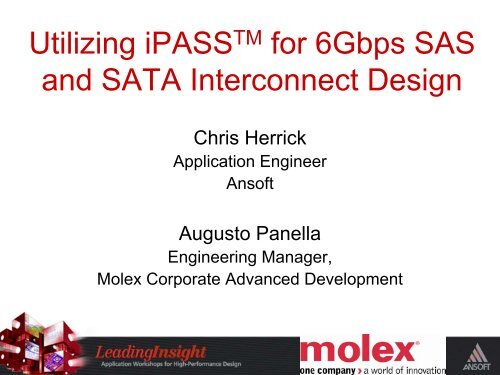
Utilizing iPass for 6Gbs SAS and SATA Interconnect Design
Utilizing iPass for 6Gbs SAS and SATA Interconnect Design
Utilizing iPass for 6Gbs SAS and SATA Interconnect Design

Create successful ePaper yourself
Turn your PDF publications into a flip-book with our unique Google optimized e-Paper software.
<strong>Utilizing</strong> iPASS TM <strong>for</strong> 6Gbps <strong>SAS</strong><br />
<strong>and</strong> <strong>SATA</strong> <strong>Interconnect</strong> <strong>Design</strong><br />
Chris Herrick<br />
Application Engineer<br />
Ansoft<br />
Augusto Panella<br />
Engineering Manager,<br />
Molex Corporate Advanced Development
Agenda<br />
• Overview of <strong>SAS</strong>/<strong>SATA</strong><br />
• Explanation of <strong>iPass</strong> TM<br />
• Simulation setup of <strong>SAS</strong>/<strong>SATA</strong> channel<br />
components<br />
• Correlation of Molex connector simulation<br />
to measurement<br />
• Conclusions
What is <strong>SAS</strong>/<strong>SATA</strong><br />
• Industry st<strong>and</strong>ards <strong>for</strong> high-speed, multi-lane internal <strong>and</strong> external<br />
systems in the network storage market<br />
• Serial rather than parallel interface<br />
• LVDS with 8b/10b encoding<br />
• <strong>SATA</strong> (Serial ATA)<br />
– Personal computer or workstation storage systems<br />
– Connections to peripherals such as Hard drives, Optical drives, removable media<br />
– 1.5 GB/s or 3.0 GB/s<br />
• <strong>SAS</strong> (Serial Attached SCSI)<br />
– High-end enterprise storage equipment (servers, RAID devices)<br />
– Per<strong>for</strong>mance, scalability, reliability <strong>and</strong> manageability.<br />
– 3.0 GB/s or 6.0 GB/s future capability of 10 GB/s by 2010
Challenges of <strong>SAS</strong>/<strong>SATA</strong><br />
• To successfully use serial technology<br />
to data rates up to 10GB/s,<br />
interconnect systems will have to be<br />
designed to provide low loss<br />
transmission paths from the host to the<br />
disk array.<br />
• Molex has developed the <strong>iPass</strong> TM<br />
<strong>Interconnect</strong> System to address the<br />
high per<strong>for</strong>mance needs <strong>for</strong> the various<br />
system connectors.<br />
• Ansoft’s suite of software can be used<br />
to design <strong>and</strong> characterize the entire<br />
channel.
<strong>iPass</strong> TM Connector <strong>Design</strong><br />
Considerations<br />
• Serial instead of parallel interfaces <strong>and</strong> interconnects = fewer lines<br />
– Smaller size <strong>for</strong> connectors<br />
– Thinner more flexible cables<br />
– Improved air flow circulation<br />
• But requires faster switching <strong>and</strong> shorter signal rise times<br />
• Which means higher frequency b<strong>and</strong>width <strong>for</strong> connectors, cable<br />
assemblies <strong>and</strong> the overall interconnect system.
<strong>iPass</strong> TM components in <strong>SATA</strong><br />
• System Schematic<br />
HDD<br />
0<br />
HDD<br />
0<br />
V8<br />
R9<br />
50<br />
R85<br />
R88<br />
logic_in<br />
enable<br />
0<br />
0<br />
50<br />
50<br />
PULLUP<br />
OUT<br />
0<br />
0<br />
System<br />
enable<br />
T4 T7<br />
T1<br />
T15 T12<br />
T18 T21 T24 T27 out_of_in<br />
T30 T33 T36<br />
0 0 0 0 0<br />
0 0 0 0 0 0 0 0 0 0 0 0 0 0 0 0 0 0 0<br />
R100 OUT<br />
logic_in<br />
logic_in<br />
out<br />
V99<br />
50<br />
PULL UP<br />
R94<br />
R95<br />
enable<br />
50<br />
50<br />
PCB<br />
PCB<br />
PCB<br />
Launch<br />
PCB<br />
Launch<br />
75784<br />
75784<br />
Cable<br />
Launch<br />
Cable<br />
Launch<br />
79576<br />
Cable<br />
79576<br />
Cable<br />
Cable<br />
Launch 75783<br />
Cable<br />
Launch<br />
PCB<br />
Launch PCB<br />
enable<br />
T62 T63 T61<br />
T65 T64<br />
T66 T67 T68 T69 out_of_in<br />
T70 T71<br />
0 0 0 0 0<br />
0 0 0 0 0 0 0 0 0 0 0 0 0 0 0 0 0<br />
logic_in<br />
pullup<br />
pulldown<br />
0<br />
0<br />
R78<br />
Controller<br />
PCB<br />
0<br />
75783 Launch PCB Controller<br />
R 110<br />
pullup<br />
pulldown<br />
out<br />
0<br />
50<br />
50<br />
PCB<br />
Launch 75586<br />
PCB<br />
Launch 75586<br />
74547<br />
Ext. Cable
<strong>iPass</strong> TM Connector 75783<br />
Creation with Ansoft’s HFSS<br />
• In the <strong>SATA</strong> system, I-Pass<br />
connector mounted to board<br />
typically soldered onto pads.<br />
• Conductors arranged in a<br />
GSSGSSG… configuration.<br />
• To launch signal into connector,<br />
50 Ω lump port pairs are used<br />
<strong>for</strong> 100 Ω differential signals.<br />
Housing<br />
Conductors<br />
PCB from cable<br />
launch<br />
Ports
Data Post-Processing<br />
• S-parameters 100 ohm differential<br />
– IL, RL, NEXT, FEXT<br />
79576<br />
Cable<br />
touchstone<br />
HFSS<br />
Cable<br />
Launch 75783<br />
HSPICE<br />
<strong>Design</strong>er<br />
PSpice<br />
Spectre<br />
PCB<br />
Launch PCB Co<br />
T12 T18 T21 T24 T27<br />
0 0 0 0 0 0 0 0 0 0<br />
logic_i<br />
enable
PCB Investigation using<br />
HFSS/<strong>Design</strong>er<br />
• <strong>iPass</strong> components will be provided by Molex;<br />
customer is responsible <strong>for</strong> PCB <strong>Design</strong><br />
• We will investigate<br />
– Manufacturing tolerances<br />
– Differential spacing<br />
– Trace bends<br />
– Via Transitions<br />
• To aid in simulation<br />
– Distributed Solve Option<br />
– Dynamic Link
Distributed Solve Option<br />
• When investigation many design variations DSO can greatly reduce<br />
solve time by solving in parallel<br />
• DSO may also be used to distribute frequency sweeps from the<br />
same project across multiple computers<br />
Host Computer<br />
…<br />
…<br />
Remote Computers<br />
(Up to 10 remote computers per Distributed Solve license)
HDD<br />
0<br />
V8<br />
<strong>Design</strong>er/HFSS Dynamic Link<br />
• <strong>Design</strong>er has the ability to dynamically link to HFSS models. This<br />
puts the EM solver inside the HFSS created circuit models.<br />
• All of the variations to the vias or microstrip transmission lines are<br />
available in the <strong>Design</strong>er environment.<br />
• See the effect changing individual parts has on the whole channel<br />
R9<br />
50<br />
R85<br />
R88<br />
logic _in<br />
enable<br />
0<br />
0<br />
50<br />
50<br />
PULL UP<br />
OUT<br />
PCB<br />
PCB<br />
Launch<br />
75784<br />
Cable<br />
Launch<br />
79576<br />
Cable<br />
Cable<br />
Launch 75783<br />
PCB<br />
Launch PCB<br />
enable<br />
T4 T7<br />
T1<br />
T15 T12<br />
T18 T21 T24 T27 out_of_in<br />
T30 T33 T36<br />
0 0 0 0 0<br />
0 0 0 0 0 0 0 0 0 0 0 0 0 0 0 0 0 0 0<br />
logic _in<br />
pullup<br />
pulldown<br />
0<br />
R78<br />
Controller<br />
out<br />
0<br />
50<br />
PCB<br />
Launch 75586<br />
74547<br />
Ext. Cable
Investigate Manufacturing Tolerances<br />
• <strong>SAS</strong>/<strong>SATA</strong> channels have st<strong>and</strong>ard layer stackup that designers<br />
must adhere to. Using the given stackup <strong>and</strong> the st<strong>and</strong>ard trace<br />
dimensions, this provides a good starting <strong>for</strong> the investigative work.<br />
• Starting with the previous design specification <strong>for</strong> <strong>SAS</strong>/<strong>SATA</strong><br />
transmission speeds, we want to be able to use the general design<br />
guidelines already established to push the next generation speeds.<br />
• From those values, we can investigate how to push more data<br />
through at faster speeds<br />
– Trace Width: 4.9mil<br />
– Differential Pair Spacing: 6.1mil<br />
– Substrate Thickness: 3.6mil<br />
– Trace Thickness: 0.6mil
Investigate Manufacturing Tolerances<br />
Over-Etching<br />
• Starting from +10% of nominal trace width (5.39mil) the effects of over<br />
etching can be seen as the top trace width is swept from 3.39mil to 5.39mil<br />
in this plot of Differential S-parameters <strong>and</strong> Differential Impedance<br />
DSO Setup<br />
11 Parametric Case<br />
11 nodes used<br />
Combined Solution Time<br />
94 min<br />
DSO Solution Time<br />
10 min<br />
Time Savings<br />
~ 9.4 times faster!
Investigate Manufacturing Tolerances<br />
Over-Etching<br />
• Starting from -10% of nominal trace width (4.41mil) the effects of<br />
over etching can be seen as the top trace width is swept from<br />
2.41mil to 4.41mil<br />
DSO Setup<br />
11 Parametric Case<br />
11 nodes used<br />
Combined Solution Time<br />
91 min<br />
DSO Solution Time<br />
11 min<br />
Time Savings<br />
~ 8.2 times faster!
Investigate Manufacturing Tolerances<br />
Differential Pair Spacing<br />
• Once a differential line width is chosen which satisfies manufacturing<br />
tolerances, HFSS is used to investigate the differential pair spacing to<br />
satisfy a 100 Ω (+/- 10%) differential impedance<br />
DSO Setup<br />
11 Parametric Case<br />
11 nodes used<br />
Combined Solution Time<br />
102 min<br />
DSO Solution Time<br />
11 min<br />
Time Savings<br />
~ 9.2 times faster!
<strong>Design</strong>er: FULL 6.97 in.<br />
Bend Models<br />
• When putting together a channel model we investigated four<br />
different modeling techniques using Ansoft Tools:<br />
<strong>Design</strong>er: Circuit Model<br />
<strong>Design</strong>er: Concatenated sections HFSS: W-Element Export
Bend Models<br />
• The 4 different methods overlaid on each other<br />
• Bends do not have a significant effect on per<strong>for</strong>mance <strong>and</strong> do not<br />
need to be modeled in future channel simulation<br />
•Green Line: Full trace length<br />
solved with Planar EM<br />
•Blue Line: Planar bend models<br />
with Circuit models <strong>for</strong> straight<br />
lengths<br />
•Red Line: Circuit model Only<br />
•Black Line: W-Element model<br />
exported from HFSS port solve<br />
IR & RL
<strong>Design</strong>ing <strong>for</strong> Improved Per<strong>for</strong>mance<br />
Via Modeling<br />
• Via modeling is the bottle neck <strong>for</strong> pushing faster data rates.<br />
• Typically, vias can be the worst degraders of signal b<strong>and</strong>width, so<br />
designing vias <strong>for</strong> optimal per<strong>for</strong>mance is critical<br />
• This fixed 4 layer stackup routed signals from top layer to bottom<br />
layer. To determine the best via routing scheme, several parametric<br />
studies can be investigated:<br />
– Differential via spacing<br />
– Via barrel radius<br />
– Percent Via fill<br />
– Antipad radius<br />
• Oval differential antipads<br />
• Individual circular antipads
HFSS Via Wizard<br />
•HFSS via models easily setup by<br />
entering dimensions in Wizard<br />
•Fully parameterized, ready<br />
to solve projects are<br />
created<br />
Antipads<br />
Backdrilling<br />
Spacing
<strong>Design</strong>ing <strong>for</strong> Improved Per<strong>for</strong>mance<br />
Via Modeling<br />
Differential Via Spacing:<br />
20mils to 40mils<br />
Via Barrel Radius: 4mils to 8mils<br />
Percent Via Fill: 10% to 100%<br />
Via Antipad Radius: 5mils to 25mils
<strong>Design</strong>ing <strong>for</strong> Improved Per<strong>for</strong>mance<br />
•The first three studies showed<br />
very little effect when the<br />
parameters were varied. These<br />
three factors proved not be<br />
critical <strong>and</strong> can be ignored in<br />
future studies<br />
Via Modeling<br />
Diff Via Spacing<br />
20mil to 40 mil<br />
2mil Steps<br />
Via Barrel Radius<br />
4mil to 8mil<br />
0.4 mil Steps<br />
Plating Percentage<br />
10 % to 100 %<br />
10% Steps
<strong>Design</strong>ing <strong>for</strong> Improved Per<strong>for</strong>mance<br />
Via Modeling<br />
• Sweeping the Oval Antipad Radius from 5mil to 25mil at 2mil<br />
Increments
<strong>Design</strong>ing <strong>for</strong> Improved Per<strong>for</strong>mance<br />
Via Modeling<br />
• What about individual circular antipads <strong>for</strong> each signal via?<br />
• Which is better, circular or oval?
<strong>Design</strong>ing <strong>for</strong> Improved Per<strong>for</strong>mance<br />
Via Modeling<br />
• Sweeping the Circular Antipad Radius from 5mil to 25mil at 1mil<br />
increments<br />
DSO Setup<br />
25 Parametric Case<br />
25 nodes used<br />
Combined Solution Time<br />
110 min<br />
DSO Solution Time<br />
7 min<br />
Time Savings<br />
~ 15.7 times faster!
– Antipad offset<br />
Additional Via Parameters<br />
– Pad dimensions<br />
– Stackup<br />
– Footprint Spacing<br />
– Blind/Through<br />
– Coax/Microstrip Launch<br />
– Square/Circular Antipads
Model What You Measure<br />
• As we just showed, varying design features can have an impact on<br />
channel per<strong>for</strong>mance<br />
• When predicting lab per<strong>for</strong>mance, it is important to include all<br />
significant details in the simulation environment<br />
• This importance of this is exemplified in a recent Molex<br />
simulation/lab correlation study of DDR3 channel model
• Only 14 pins of mated socket<br />
modeled in HFSS.<br />
• Lump ports utilized.<br />
• Simulation condition:<br />
– Signal-Gnd-Ratio � 2:1<br />
– PCB <strong>and</strong> Module<br />
Simulation Setup<br />
• Material � FR4 (ε r = 4.4)<br />
• Trace width � 18mils<br />
(0.4572mm)<br />
• Stack height � 10mils<br />
(0.254mm)<br />
• S-parameter model exported <strong>and</strong><br />
parameters evaluated in <strong>Design</strong>er.<br />
240 pin<br />
DDR3 SMT<br />
Socket<br />
2 rows x 7 columns<br />
pin matrix
• Equipment List<br />
– Tektronix<br />
Digital<br />
Sampling<br />
Oscilloscop<br />
e �<br />
CSA8000B<br />
– Tektronix<br />
Differential<br />
TDR<br />
Sampling<br />
Heads �<br />
80E04<br />
• Measurement<br />
Conditions<br />
– TDR<br />
measured<br />
with 100ps<br />
risetime at<br />
input of DUT<br />
Test Fixture <strong>Design</strong>
Simulation<br />
Measurement<br />
Spec<br />
Initial Correlation Results<br />
No Resonance<br />
Observed in<br />
Measured<br />
results<br />
No Resonance<br />
Observed in<br />
Measured results<br />
Insertion Loss<br />
Return Loss<br />
Near-end Crosstalk<br />
No Resonance<br />
Observed in<br />
Measured results<br />
Far-end Crosstalk
Initial Vs. Revised<br />
Simulation Setup<br />
• Simulation model was compared against Gerber files used <strong>for</strong><br />
fixture fabrication<br />
• Vias were included in fixture but missing in simulation model<br />
setup<br />
• Simulation was corrected <strong>and</strong> reran<br />
Vias added<br />
Vias missing.<br />
to<br />
missing.<br />
to both<br />
Shorting pads<br />
PCB<br />
pads<br />
PCB <strong>and</strong><br />
were only<br />
module<br />
only<br />
module card<br />
used at<br />
PCB
Simulation<br />
Measurement<br />
Final Correlation<br />
Spec<br />
No Resonance<br />
Observed in<br />
new simulated<br />
results<br />
Insertion Loss<br />
Return Loss<br />
No Resonance<br />
Observed in<br />
new simulated<br />
No Resonance<br />
results<br />
Observed in<br />
Near-end Crosstalk<br />
new simulated<br />
results<br />
Far-end Crosstalk
• Molex <strong>iPass</strong> TM interconnect system has been designed using HFSS to<br />
provide seamless connection between components<br />
• When designing <strong>for</strong> faster data, such as <strong>SATA</strong>/<strong>SAS</strong>, having accurate<br />
models <strong>for</strong> the transmission lines <strong>and</strong> vias is critical to first pass<br />
success.<br />
• Using automation features such as DSO, Dynamic Link <strong>and</strong> the Via<br />
Wizard, hundreds of iterations can be efficiently run to investigate<br />
manufacturing tolerances design properties.<br />
• Always model what you measure<br />
• <strong>Design</strong> Kit will be available on Ansoft.com. Tentatively it will include:<br />
– <strong>iPass</strong> TM component models<br />
– HFSS Via Wizard<br />
Conclusion<br />
– Parametrized HFSS Transmission lines<br />
– Parameterized <strong>Design</strong>er Channel model