LTC3851A - Synchronous Step-Down Switching Regulator Controller
LTC3851A - Synchronous Step-Down Switching Regulator Controller
LTC3851A - Synchronous Step-Down Switching Regulator Controller

Create successful ePaper yourself
Turn your PDF publications into a flip-book with our unique Google optimized e-Paper software.
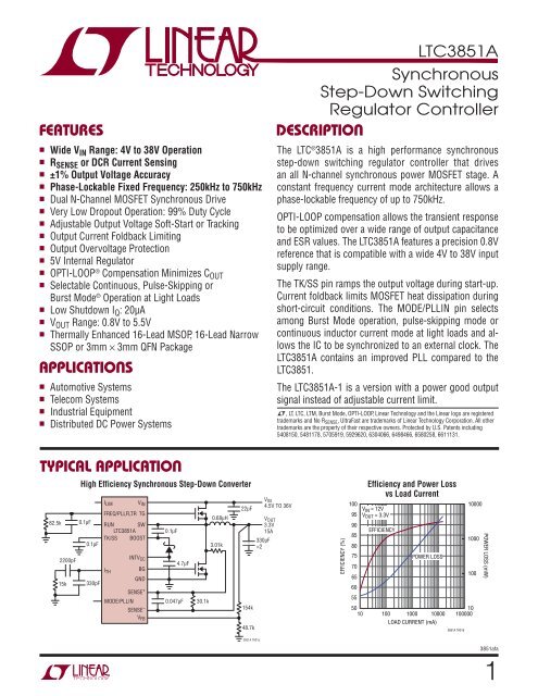
Featuresn Wide V IN Range: 4V to 38V Operationn R SENSE or DCR Current Sensingn ±1% Output Voltage Accuracyn Phase-Lockable Fixed Frequency: 250kHz to 750kHzn Dual N-Channel MOSFET <strong>Synchronous</strong> Driven Very Low Dropout Operation: 99% Duty Cyclen Adjustable Output Voltage Soft-Start or Trackingn Output Current Foldback Limitingn Output Overvoltage Protectionn 5V Internal <strong>Regulator</strong>n OPTI-LOOP ® Compensation Minimizes C OUTn Selectable Continuous, Pulse-Skipping orBurst Mode ® Operation at Light Loadsn Low Shutdown I Q : 20µAn V OUT Range: 0.8V to 5.5Vn Thermally Enhanced 16-Lead MSOP, 16-Lead NarrowSSOP or 3mm × 3mm QFN PackageApplicationsn Automotive Systemsn Telecom Systemsn Industrial Equipmentn Distributed DC Power Systems<strong>LTC3851A</strong><strong>Synchronous</strong><strong>Step</strong>-<strong>Down</strong> <strong>Switching</strong><strong>Regulator</strong> <strong>Controller</strong>DescriptionThe LTC ® 3851A is a high performance synchronousstep-down switching regulator controller that drivesan all N-channel synchronous power MOSFET stage. Acon stant frequency current mode architecture allows aphase‐lockable frequency of up to 750kHz.OPTI-LOOP compensation allows the transient responseto be optimized over a wide range of output capacitanceand ESR values. The <strong>LTC3851A</strong> features a precision 0.8Vreference that is compatible with a wide 4V to 38V inputsupply range.The TK/SS pin ramps the output voltage during start‐up.Current foldback limits MOSFET heat dissipation duringshort-circuit conditions. The MODE/PLLIN pin selectsamong Burst Mode operation, pulse-skipping mode orcontinuous inductor current mode at light loads and allowsthe IC to be synchronized to an external clock. The<strong>LTC3851A</strong> contains an improved PLL compared to theLTC3851.The <strong>LTC3851A</strong>-1 is a version with a power good outputsignal instead of adjustable current limit.L, LT, LTC, LTM, Burst Mode, OPTI-LOOP, Linear Technology and the Linear logo are registeredtrademarks and No R SENSE , UltraFast are trademarks of Linear Technology Corporation. All othertrademarks are the property of their respective owners. Protected by U.S. Patents including5408150, 5481178, 5705919, 5929620, 6304066, 6498466, 6580258, 6611131.Typical ApplicationHigh Efficiency <strong>Synchronous</strong> <strong>Step</strong>-<strong>Down</strong> ConverterI LIM V INFREQ/PLLFLTR TG82.5k 0.1µFRUN SW<strong>LTC3851A</strong>TK/SS BOOST0.1µF2200pF15k330pFI THINTV CCBGGNDSENSE +MODE/PLLINSENSE –V FB0.1µF4.7µF0.047µF30.1k0.68µH3.01k22µF154k48.7kV IN4.5V TO 36VV OUT3.3V15A330µF×2EFFICIENCY (%)1009590858075706560555010Efficiency and Power Lossvs Load CurrentV IN = 12VV OUT = 3.3VEFFICIENCYPOWER LOSS10100 1000 10000 100000LOAD CURRENT (mA)3851A TA01b100001000100POWER LOSS (mW)3851A TA01a3851afa1
<strong>LTC3851A</strong>Absolute Maximum RatingsInput Supply Voltage (V IN ).......................... 40V to –0.3VTopside Driver Voltage (BOOST)................. 46V to –0.3VSwitch Voltage (SW)......................................40V to –5VINTV CC , (BOOST – SW), RUN....................... 6V to –0.3VTK/SS, I LIM ............................................INTV CC to –0.3VSENSE + , SENSE – ........................................... 6V to –0.3VMODE/PLLIN, FREQ/PLLFLTR...............INTV CC to –0.3VI TH , V FB Voltages........................................... 3V to –0.3V(Note 1)INTV CC Peak Output Current...................................50mAOperating Junction Temperature Range (Notes 2, 3)E-Grade, I-Grade................................. –40°C to 125°CH-Grade.............................................. –40°C to 150°CMP-Grade........................................... –55°C to 150°CStorage Temperature Range...................–65°C to 150°CLead Temperature (Soldering, 10 sec)GN/MSE.............................................................300°CPin ConfigurationMODE/PLLINFREQ/PLLFLTRRUNTK/SSI THFBSENSE –SENSE +12345678TOP VIEW16 SW15 TG14 BOOST13 V IN12 INTV CC11 BG10 GND9 I LIMGN PACKAGE16-LEAD PLASTIC SSOP NARROWT JMAX = 125°C, θ JA = 110°C/W116710SENSE + 894562317GND1312111514MODE/PLLINFREQ/PLLFLTRRUNTK/SSI THFBSENSE –TOP VIEWMSE PACKAGE16-LEAD PLASTIC MSOPT JMAX = 125°C, θ JA = 35°C/W TO 40°C/WEXPOSED PAD (PIN 17) IS GND,MUST BE SOLDERED TO PCBSWTGBOOSTV ININTV CCBGGNDI LIMRUNTK/SSI THFB1234TOP VIEWFREQ/PLLFLTRMODE/PLLINSWTG16 15 14 1317GND5 6 7 8SENSE –SENSE +I LIMGND12 BOOST11 V IN10 INTV CC9 BGUD PACKAGE16-LEAD (3mm × 3mm) PLASTIC QFNT JMAX = 125°C, θ JA = 68°C/W, θ JC = 4.2°C/WEXPOSED PAD (PIN 17) IS GND,MUST BE SOLDERED TO PCBOrder InformationLEAD FREE FINISH TAPE AND REEL PART MARKING* PACKAGE DESCRIPTION TEMPERATURE RANGE<strong>LTC3851A</strong>EGN#PBF <strong>LTC3851A</strong>EGN#TRPBF 3851A 16-Lead Plastic SSOP –40°C to 125°C<strong>LTC3851A</strong>IGN#PBF <strong>LTC3851A</strong>IGN#TRPBF 3851A 16-Lead Plastic SSOP –40°C to 125°C<strong>LTC3851A</strong>EMSE#PBF <strong>LTC3851A</strong>EMSE#TRPBF 3851A 16-Lead Plastic MSOP –40°C to 125°C<strong>LTC3851A</strong>IMSE#PBF <strong>LTC3851A</strong>IMSE#TRPBF 3851A 16-Lead Plastic MSOP –40°C to 125°C<strong>LTC3851A</strong>HMSE#PBF <strong>LTC3851A</strong>HMSE#TRPBF 3851A 16-Lead Plastic MSOP –40°C to 150°C<strong>LTC3851A</strong>MPMSE#PBF <strong>LTC3851A</strong>MPMSE#TRPBF 3851A 16-Lead Plastic MSOP –55°C to 150°C<strong>LTC3851A</strong>EUD#PBF <strong>LTC3851A</strong>EUD#TRPBF LFPZ 16-Lead (3mm × 3mm) Plastic QFN –40°C to 125°C<strong>LTC3851A</strong>IUD#PBF <strong>LTC3851A</strong>IUD#TRPBF LFPZ 16-Lead (3mm × 3mm) Plastic QFN –40°C to 125°CConsult LTC Marketing for parts specified with wider operating temperature ranges. *The temperature grade is identified by a label on the shipping container.Consult LTC Marketing for information on non-standard lead based finish parts.For more information on lead free part marking, go to: http://www.linear.com/leadfree/For more information on tape and reel specifications, go to: http://www.linear.com/tapeandreel/23851afa
Electrical Characteristics<strong>LTC3851A</strong>The l denotes the specifications which apply over the specified operatingtemperature range, otherwise specifications are at T A = 25°C (Note 2). V IN = 15V, V RUN = 5V unless otherwise noted.SYMBOL PARAMETER CONDITIONS MIN TYP MAX UNITSMain Control LoopsV IN Operating Input Voltage Range l 4 38 VV FB Regulated Feedback Voltage I TH = 1.2V (Note 4) 0°C to 85°CI TH = 1.2V (Note 4) –40°C to 125°CI TH = 1.2V (Note 4) –40°C to 150°CI TH = 1.2V (Note 4) –55°C to 150°Cllll0.7920.7880.7880.7880.800 0.8080.8120.8120.812I FB Feedback Current (Note 4) –10 –50 nAV REFLNREG Reference Voltage Line Regulation V IN = 6V to 38V (Note 4) 0.002 0.02 %/VV LOADREG Output Voltage Load Regulation (Note 4) Measured in Servo Loop,∆I TH = 1.2V to 0.7V(Note 4) Measured in Servo Loop,∆I TH = 1.2V to 0.7V (H-Grade, MP-Grade)ll0.01 0.10.2%%(Note 4) Measured in Servo Loop,∆I TH = 1.2V to 1.6V(Note 4) Measured in Servo Loop,∆I TH = 1.2V to 1.6V (H-Grade, MP-Grade)ll–0.01 –0.1–0.2%%g m Transconductance Amplifier g m I TH = 1.2V, Sink/Source = 5µA (Note 4) 2 mmhog m GBW Transconductance Amp Gain Bandwidth I TH = 1.2V (Note 8) 3 MHzI Q Input DC Supply CurrentNormal Mode(Note 5)V RUN = 5V1.2mAShutdownV RUN = 0V25 50 µAUVLO Undervoltage Lockout on INTV CC V INTVCC Ramping <strong>Down</strong> 3.25 VUVLO Hys UVLO Hysteresis 0.4 VV OVL Feedback Overvoltage Lockout V FB with Respect to Set Regulated Voltage V FB Ramping 7.5 10 12.5 %Positive (OV)I SENSE SENSE Pins Current ±1 ±2 µAI TK/SS Soft-Start Charge Current V TK/SS = 0V 0.6 1 2 µAV RUN RUN Pin On—Threshold V RUN Rising l 1.10 1.22 1.35 VV RUNHYS RUN Pin On—Hysteresis 120 mVV SENSE(MAX) Maximum Current Sense Threshold V FB = 0.7V, V SENSE = 3.3V, I LIM = 0VV FB = 0.7V, V SENSE = 3.3V, I LIM = 0V (H-/MP-Grade)V FB = 0.7V, V SENSE = 3.3V, I LIM = FloatV FB = 0.7V, V SENSE = 3.3V, I LIM = Float (H-/MP-Grade)V FB = 0.7V, V SENSE = 3.3V, I LIM = INTV CCV FB = 0.7V, V SENSE = 3.3V, I LIM = INTV CC (H-/MP-Grade)TG R UP TG Driver Pull-Up On-Resistance TG High 2.2 ΩTG R DOWN TG Driver Pull-<strong>Down</strong> On-Resistance TG Low 1.2 ΩBG R UP BG Driver Pull-Up On-Resistance BG High 2.1 ΩBG R DOWN BG Driver Pull-<strong>Down</strong> On-Resistance BG Low 1.1 ΩTG t rTG t fBG trBG tfTG/BG t 1DBG/TG t 2DTG Transition TimeRise TimeFall TimeBG Transition TimeRise TimeFall TimeTop Gate Off to Bottom Gate On DelayBottom Switch-On Delay TimeBottom Gate Off to Top Gate On Delay TopSwitch-On Delay Time(Note 6)C LOAD = 3300pFC LOAD = 3300pF(Note 6)C LOAD = 3300pFC LOAD = 3300pFC LOAD = 3300pF Each Driver(Note 6)C LOAD = 3300pF Each Driver(Note 6)llllll201540356560305380252525254045657095100VVVVmVmVmVmVmVmVnsnsnsns30 ns30 nst ON(MIN) Minimum On-Time (Note 7) 90 ns3851afa3
<strong>LTC3851A</strong>Electrical Characteristics The l denotes the specifications which apply over the specified operatingtemperature range, otherwise specifications are at T A = 25°C (Note 2). V IN = 15V, V RUN = 5V unless otherwise noted.SYMBOL PARAMETER CONDITIONS MIN TYP MAX UNITSINTV CC Linear <strong>Regulator</strong>V INTVCC Internal V CC Voltage 6V < V IN < 38V 4.8 5 5.2 VV LDO INT INTV CC Load Regulation I CC = 0mA to 50mA 0.5 2 %Oscillator and Phase-Locked Loopf NOM Nominal Frequency R FREQ = 60k 460 500 540 kHzf LOW Lowest Frequency R FREQ = 160k 205 235 265 kHzf HIGH Highest Frequency R FREQ = 36k 690 750 810 kHzR MODE/PLLIN MODE/PLLIN Input Resistance 100 kΩf MODE MODE/PLLIN Minimum Input FrequencyMODE/PLLIN Maximum Input FrequencyV MODE = External ClockV MODE = External Clock250750kHzkHzI FREQPhase Detector Output CurrentSinking CapabilitySourcing Capabilityf MODE > f OSC–90f MODE < f OSC 75µAµANote 1: Stresses beyond those listed under Absolute Maximum Ratings maycause permanent damage to the device. Exposure to any Absolute MaximumRating condition for extended periods may affect device reliability and lifetime.Note 2: The <strong>LTC3851A</strong> is tested under pulsed load conditions such thatT A ≈ T J . The <strong>LTC3851A</strong>E is guaranteed to meet performance specificationsfrom 0°C to 85°C junction temperature. Specifications over the –40°Cto 125°C operating junction temperature range are assured by design,characterization and correlation with statistical process controls. The<strong>LTC3851A</strong>I is guaranteed to meet specifications over the –40°C to 125°Coperating junction temperature range, the <strong>LTC3851A</strong>H is guaranteedover the –40°C to 150°C operating junction temperature range and the<strong>LTC3851A</strong>MP is tested and guaranteed over the –55°C to 150°C operatingjunction temperature range. High junction temperatures degrade operatinglifetimes; operating lifetime is derated for junction temperatures greaterthan 125°C. Note that the maximum ambient temperature consistent withthese specifications is determined by specific operating conditions inconjunction with board layout, the rated package thermal impedance andother environmental factors.Note 3: T J is calculated from the ambient temperature T A and powerdissipation P D according to the following formulas:<strong>LTC3851A</strong>GN: T J = T A + (P D • 110°C/W)<strong>LTC3851A</strong>UD: T J = T A + (P D • 68°C/W)<strong>LTC3851A</strong>MSE: T J = T A + (P D • 40°C/W)Note 4: The <strong>LTC3851A</strong> is tested in a feedback loop that servos V ITH to aspecified voltage and measures the resultant V FB .Note 5: Dynamic supply current is higher due to the gate charge beingdelivered at the switching frequency. See Applications Information.Note 6: Rise and fall times are measured using 10% and 90% levels. Delaytimes are measured using 50% levels. Rise and fall times are assured bydesign, characterization and correlation with statistical process controls.Note 7: The minimum on-time condition is specified for an inductorpeak-to-peak ripple current ~40% of I MAX (see Minimum On-TimeConsiderations in the Applications Information section).Note 8: Guaranteed by design; not tested in production.Typical Performance CharacteristicsEFFICIENCY(%)48070605040302010Efficiency vs Output Currentand Mode100VIN = 12V90 V OUT = 1.5V010BURSTPULSESKIPCCM100 1000 10000 100000LOAD CURRENT (mA)3851A G01EFFICIENCY(%)100908070605040302010010Efficiency vs Output Currentand ModeBURSTPULSESKIPCCMV IN = 12VV OUT = 3.3VFIGURE 11 CIRCUIT100 1000 10000 100000LOAD CURRENT (mA)3851A G02EFFICIENCY (%)100908070605040302010010Efficiency vs Output Currentand ModeBURSTPULSESKIPCCMV IN = 12VV OUT = 5V100 1000 10000 100000LOAD CURRENT (mA)3851A G033851afa
Typical Performance Characteristics<strong>LTC3851A</strong>EFFICIENCY (%)1009590858075704Efficiency and Power Lossvs Input VoltageEFFICIENCY,I OUT = 5APOWER LOSS,I OUT = 5AEFFICIENCY,I OUT = 0.5APOWER LOSS,I OUT = 0.5AV IN = 12VV OUT = 3.3VFIGURE 11 CIRCUIT1008 12 16 20 24 28 32INPUT VOLTAGE (V)3851A G04100001000POWER LOSS (mW)I LOAD5A/DIV0.2A TO 7.5AI L5A/DIVV OUT100mV/DIVAC-COUPLEDLoad <strong>Step</strong>(Burst Mode Operation)V OUT = 1.5V 100µs/DIVV IN = 12VFIGURE 11 CIRCUIT3851A G05I LOAD5A/DIV0.2A TO 7.5ALoad <strong>Step</strong>(Forced Continuous Mode)I LOAD5A/DIV0.2A TO 7.5ALoad <strong>Step</strong>(Pulse-Skipping Mode)I L5A/DIVI L5A/DIVV OUT100mV/DIVAC-COUPLEDV OUT100mV/DIVAC-COUPLEDV OUT = 1.5V 100µs/DIVV IN = 12VFIGURE 11 CIRCUIT3851A G06V OUT = 1.5V 100µs/DIVV IN = 12VFIGURE 11 CIRCUIT3851A G07Inductor Current at Light LoadStart-Up with Prebiased Outputat 2VCoincident Tracking with MasterSupplyFORCEDCONTINOUSMODE5A/DIVBurst ModeOPERATION5A/DIVPULSE-SKIPPINGMODE5A/DIVV OUT2V/DIVV FB0.5V/DIVTK/SS0.5V/DIVV MASTER0.5V/DIVV OUT2A LOAD0.5V/DIVV OUT = 1.5V 1µs/DIVV IN = 12VI LOAD = 1mAFIGURE 11 CIRCUIT3851A G0820ms/DIV3851A G0910ms/DIV3851A G103851afa5
<strong>LTC3851A</strong>Typical Performance CharacteristicsV MASTER0.5V/DIVV OUT2A LOAD0.5V/DIVRatiometric Tracking with MasterSupply10ms/DIV3851A G11SUPPLY CURRENT (mA)3.02.52.01.51.00.504Input DC Supply Currentvs Input Voltage8 12 16 20 24 28 32 36 40INPUT VOLTAGE (V)3851A G12INTV CC VOLTAGE (V)INTV CC Line Regulation5.35.1 I LOAD = 0mA4.9I LOAD = 25mA4.74.54.34.13.93.73.54 8 12 16 20 24 28 32 36 40INPUT VOLTAGE (V)3851A G13V SENSE THRESHOLD (mV)90807060504030201000Maximum Current Sense Thresholdvs Common Mode VoltageI LIM = INTV CCI LIM = FLOATI LIM = GND0.5 1 1.5 2 2.5 3 3.5 4 4.5 5V SENSE COMMON MODE VOLTAGE (V)V SENSE (mV)Maximum Peak Current SenseThreshold vs I TH Voltage90DUTY CYCLE RANGE: 0% TO 100%8070I LIM = INTV CC6050I LIM = FLOAT4030I20LIM = GND100–10–200 0.2 0.4 0.6 0.8 1.0 1.2 1.4 1.6 1.8 2.0 2.2 2.4V ITH (V)V SENSE (mV)60504030Burst Mode Peak Current SenseThreshold vs I TH VoltageMAXIMUIM20MINIMUIM10 I LIM = FLOATBURST COMPARATOR FALLING THESHOLD:V0 ITH = 0.4V0.4 0.6 0.8 1.0 1.2 1.4 1.6 1.8 2.0 2.2 2.4V ITH (V)90Maximum Current SenseThreshold vs Duty Cycle3851A G14903851A G15Maximum Current SenseThreshold vs Feedback Voltage(Current Foldback)1.5TK/SS Pull-Up Currentvs Temperature3851A G16CURRENT SENSE THRESHOLD (mV)80 I LIM = INTV CC7060504030201000I LIM = FLOATI LIM = GND20 40 60 80 100DUTY CYCLE (%)MAXIMUM V SENSE (mV)807060504030201000I LIM = INTV CCI LIM = FLOATI LIM = GND0.1 0.2 0.3 0.4 0.5 0.6 0.7FEEDBACK VOLTAGE (V)0.8TK/SS CURRENT (µA)1.41.31.21.11.00.90.80.70.60.5–75–50 –25 0 25 50 75 100 125 150TEMPERATURE (°C)3851A G173851A G183851A G1963851afa
Typical Performance Characteristics<strong>LTC3851A</strong>1.4Shutdown (RUN) Thresholdvs Temperature806Regulated Feedback Voltagevs Temperature900Oscillator Frequencyvs TemperatureRUN PIN VOLTAGE (V)1.31.21.11.0RUN RISING THRESHOLD (ON)RUN FALLING THRESHOLD (OFF)REGULATED FEEDBACK VOLTAGE (mV)804802800798796FREQUENCY (kHz)800700600500400300R PLLLPF = 36kR PLLLPF = 60kR PLLLPF = 160k0.9–75 –50 –250 25 50 75 100 125 150TEMPERATURE (°C)794–75 –50–25 0 25 50 75 100 125 150TEMPERATURE (°C)200–75 –50–25 0 25 50 75 100 125 150TEMPERATURE (°C)3851A G203851A G213851A G22FREQUENCY (kHz)4204154104054003953903853805Oscillator Frequencyvs Input VoltageR FREQ = 80k10 15 20 25 30 35 40INPUT VOLTAGE (V)INTV CC VOLTAGE AT UVLO THRESHOLD (V)54321Undervoltage Lockout Threshold(INTV CC ) vs Temperature0–75 –50 –25INTV CC RAMPING UPINTV CC RAMPING DOWN0 25 50 75 100 125 150TEMPERATURE (°C)SHUTDOWN SUPPLY CURRENT (µA)40353025201510500Shutdown Input DC SupplyCurrent vs Input Voltage5 10 15 20 25 30 35INPUT VOLTAGE (V)403851A G233851A G243851A G25SHUTDOWN INPUT DC SUPPLY CURRENT (µA)403530252015105Shutdown Input DC SupplyCurrent vs Temperature0–75 –50 –25 0 25 50TEMPERATURE (°C)75 100 125 150INPUT DC SUPPLY CURRENT (mA)Input DC Supply Currentvs Temperature3.02.52.01.51.00.50–75 –50 –25 0 25 50 75 100 125 150TEMPERATURE (°C)MAXIMUM V SENSE (mV)908070605040302010Maximum Current SenseThreshold vs INTV CC Voltage03.2 3.4 3.6I SET = INTV CCI SET = FLOATI SET = GND3.8 4.0 4.2 4.4 4.6 4.8 5.0INTV CC VOLTAGE(V)3851A G263851A G273851A G283851afa7
<strong>LTC3851A</strong>Pin Functions (GN and MSE/UD)MODE/PLLIN (Pin 1/Pin 15): Forced Continuous Mode,Burst Mode or Pulse-Skipping Mode Selection Pin and ExternalSynchronization Input to Phase Detector Pin. Connectthis pin to INTV CC to force continuous conduction modeof operation. Connect to GND to enable pulse-skippingmode of operation. To select Burst Mode operation, tiethis pin to INTV CC through a resistor no less than 50k,but no greater than 250k. A clock on the pin will causethe controller to operate in forced continuous mode ofoperation and synchronize the internal oscillator.FREQ/PLLFLTR (Pin 2/Pin 16): The phase-locked loop’slowpass filter is tied to this pin. Alternatively, a resistorcan be connected between this pin and GND to vary thefrequency of the internal oscillator.RUN (Pin 3/Pin 1): Run Control Input. A voltage above1.22V on this pin turns on the IC. However, forcing thispin below 1.1V causes the IC to shut down the IC. Thereis a 2μA pull-up current on this pin.TK/SS (Pin 4/Pin 2): Output Voltage Tracking and Soft-StartInput. A capacitor to ground at this pin sets the ramp ratefor the output voltage. An internal soft-start current of of1μA charges this capacitor.I TH (Pin 5/Pin 3): Current Control Threshold and ErrorAmplifier Compensation Point. The current comparatortripping threshold increases with its I TH control voltage.FB (Pin 6/Pin 4): Error Amplifier Feedback Input. This pinreceives the remotely sensed feedback voltage from anexternal resistive divider across the output.SENSE – (Pin 7/Pin 5): Current Sense Comparator InvertingInput. The (–) input to the current comparator is connectedto the output.SENSE + (Pin 8/Pin 6): Current Sense Comparator NoninvertingInput. The (+) input to the current comparatoris normally connected to the DCR sensing network orcurrent sensing resistor.I LIM (Pin 9/Pin 7): Current Comparator Sense VoltageRange Input. Tying this pin to GND, FLOAT or INTV CCselects the maximum current sense threshold from threedif ferent levels.GND (Pin 10/Pin 8, Exposed Pad Pin 17): Ground. Allsmall-signal components and compensation componentsshould be Kelvin connected to this ground. The (–) terminalof CV CC and the (–) terminal of C IN should be closely connectedto this pin. The exposed pad should be solderedto ground for good thermal conductivity.BG (Pin 11/Pin 9): Bottom Gate Driver Output. This pindrives the gate of the bottom N-channel MOSFET betweenGND and INTV CC .INTV CC (Pin 12/Pin 10): Internal 5V <strong>Regulator</strong> Output. Thecontrol circuit is powered from this voltage. Decouple thispin to GND with a minimum 2.2μF low ESR tantalum orceramic capacitor.V IN (Pin 13/Pin 11): Main Input Supply. Decouple this pinto GND with a capacitor.BOOST (Pin 14/Pin 12): Boosted Floating Driver Supply.The (+) terminal of the boost-strap capacitor is connectedto this pin. This pin swings from a diode voltage dropbelow INTV CC up to V IN + INTV CC .TG (Pin 15/Pin 13): Top Gate Driver Output. This is theoutput of a floating driver with a voltage swing equal toINTV CC superimposed on the switch node voltage.SW (Pin 16/Pin 14): Switch Node Connection to the Inductor.Voltage swing at this pin is from a Schottky diode(external) voltage drop below ground to V IN .83851afa
–+<strong>LTC3851A</strong>Functional DiagramFREQ/PLLFLTRMODE/PLLINPLL-SYNC100kMODE/SYNCDETECTOSC+–5kSR Q–+I REV0.8V– +PULSE SKIPONBURSTENSWITCHLOGICANDANTI-SHOOTTHROUGH5V REGV IN+C INBOOSTTG C BM1SWSENSE +D BL1SENSE –RUNINTV CC+V OUTC OUTOVBGM2V IN2µASLOPE COMPENSATIONINTV CCUVLO1100kR20.88VR1EASS– +RUN– + +0.64V1.22VI LIMI THBI CMPC C1C VCCGNDV FBV INSLEEPOV0.8VREF– +1µA– +0.4VI THRUNTK/SS3851A FDR CC SS3851afa9
<strong>LTC3851A</strong>OperationMain Control LoopThe <strong>LTC3851A</strong> is a constant frequency, current modestep-down controller. During normal operation, the topMOSFET is turned on when the clock sets the RS latch,and is turned off when the main current comparator, I CMP ,resets the RS latch. The peak inductor current at whichI CMP resets the RS latch is controlled by the voltage onthe I TH pin, which is the output of the error amplifier, EA.The V FB pin receives the voltage feedback signal, which iscompared to the internal reference voltage by the EA. Whenthe load current increases, it causes a slight decrease inV FB relative to the 0.8V reference, which in turn causes theI TH voltage to increase until the average inductor currentmatches the new load current. After the top MOSFET hasturned off, the bottom MOSFET is turned on until eitherthe inductor current starts to reverse, as indicated by thereverse current comparator, I REV , or the beginning of thenext cycle.INTV CC PowerPower for the top and bottom MOSFET drivers and mostother internal circuitry is derived from the INTV CC pin. Aninternal 5V low dropout linear regulator supplies INTV CCpower from V IN .The top MOSFET driver is biased from the floating bootstrapcapacitor, C B , which normally recharges during eachoff cycle through an external diode when the top MOSFETturns off. If the input voltage, V IN , decreases to a voltageclose to V OUT , the loop may enter dropout and attemptto turn on the top MOSFET continuously. The dropoutdetec tor detects this and forces the top MOSFET off forabout 1/10 of the clock period every tenth cycle to allowC B to recharge. However, it is recommended that there isalways a load present during the drop-out transition toensure C B is recharged.Shutdown and Start-Up (RUN and TK/SS)The <strong>LTC3851A</strong> can be shut down using the RUN pin. Pullingthis pin below 1.1V disables the controller and mostof the internal circuitry, including the INTV CC regulator.Releasing the RUN pin allows an internal 2µA current topull up the pin and enable that control ler. Alternatively,the RUN pin may be externally pulled up or driven directlyby logic. Be careful not to exceed the absolute maximumrating of 6V on this pin.The start-up of the controller’s output voltage, V OUT , iscontrolled by the voltage on the TK/SS pin. When thevoltage on the TK/SS pin is less than the 0.8V internalreference, the <strong>LTC3851A</strong> regulates the V FB voltage to theTK/SS pin voltage instead of the 0.8V reference. This allowsthe TK/SS pin to be used to program a soft-start byconnecting an external capacitor from the TK/SS pin toGND. An internal 1µA pull-up current charges this capacitorcreating a voltage ramp on the TK/SS pin. As the TK/SSvoltage rises linearly from 0V to 0.8V (and beyond), theoutput voltage V OUT rises smoothly from zero to its finalvalue. Alternatively, the TK/SS pin can be used to causethe start-up of V OUT to track another supply. Typically,this requires connecting to the TK/SS pin an externalresistor divider from the other supply to ground (see theApplica tions Information section). When the RUN pinis pulled low to disable the controller, or when INTV CCdrops below its undervoltage lockout threshold of 3.2V,the TK/SS pin is pulled low by an internal MOSFET. Whenin undervoltage lockout, the controller is disabled and theexternal MOSFETs are held off.Light Load Current Operation (Burst Mode Operation,Pulse-Skipping or Continuous Conduction)The <strong>LTC3851A</strong> can be enabled to enter high efficiencyBurst Mode operation, constant frequency pulse-skippingmode or forced continuous conduction mode. To selectforced continuous operation, tie the MODE/PLLIN pin toINTV CC . To select pulse-skipping mode of operation, floatthe MODE/PLLIN pin or tie it to GND. To select Burst Modeoperation, tie MODE/PLLIN to INTV CC through a resistorno less than 50k, but no greater than 250k.When the controller is enabled for Burst Mode operation,the peak current in the inductor is set to approximatelyone-forth of the maximum sense voltage even thoughthe voltage on the I TH pin indicates a lower value. If theaverage inductor current is higher than the load current,103851afa
Operationthe error amplifier, EA, will decrease the voltage on the I THpin. When the I TH voltage drops below 0.4V, the internalsleep signal goes high (enabling sleep mode) and bothexternal MOSFETs are turned off.In sleep mode, the load current is supplied by the outputcapacitor. As the output voltage decreases, the EA’s outputbegins to rise. When the output voltage drops enough, thesleep signal goes low, and the controller resumes normaloperation by turning on the top external MOSFET on thenext cycle of the internal oscillator. When a controller isenabled for Burst Mode operation, the inductor current isnot allowed to reverse. The reverse current comparator,I REV , turns off the bottom external MOSFET just before theinductor current reaches zero, preventing it from reversingand going negative. Thus, the controller operates indiscontinuous operation. In forced continuous operation,the inductor current is allowed to reverse at light loads orunder large transient conditions. The peak inductor currentis determined by the voltage on the I TH pin, just as innormal operation. In this mode the efficiency at light loadsis lower than in Burst Mode operation. However, continuousmode has the advantages of lower output ripple andless interference to audio circuitry.When the MODE/PLLIN pin is connected to GND, the<strong>LTC3851A</strong> operates in PWM pulse-skipping mode at lightloads. At very light loads the current comparator, I CMP , mayremain tripped for several cycles and force the external topMOSFET to stay off for the same number of cycles (i.e.,skipping pulses). The inductor current is not allowed toreverse (discontinuous operation). This mode, like forcedcontinuous operation, exhibits low output ripple as well aslow audio noise and reduced RF interference as comparedto Burst Mode operation. It provides higher low currentefficiency than forced continuous mode, but not nearly ashigh as Burst Mode operation.<strong>LTC3851A</strong>Frequency Selection and Phase-Locked Loop(FREQ/PLLFLTR and MODE/PLLIN Pins)The selection of switching frequency is a trade-off betweenefficiency and component size. Low frequency operationincreases efficiency by reducing MOSFET switchinglosses, but requires larger inductance and/or capacitanceto main tain low output ripple voltage. The switching frequencyof the <strong>LTC3851A</strong> can be selected using the FREQ/PLLFLTR pin. If the MODE/PLLIN pin is not being drivenby an external clock source, the FREQ/PLLFLTR pin canbe used to program the controller’s operating frequencyfrom 250kHz to 750kHz.A phase-locked loop (PLL) is available on the <strong>LTC3851A</strong>to synchronize the internal oscillator to an external clocksource that is connected to the MODE/PLLIN pin. Thecontroller operates in forced continuous mode of operationwhen it is synchronized. A series RC should be connectedbetween the FREQ/PLLFLTR pin and GND to serve as thePLL’s loop filter. It is suggested that the external clock beapplied before enabling the controller unless a secondresistor is connected in parallel with the series RC network.The second resistor prevents very low switching frequencyoperation if the controller is enabled before the clock.Output Overvoltage ProtectionAn overvoltage comparator, OV, guards against transientovershoots (>10%) as well as other more serious conditionsthat may overvoltage the output. In such cases,the top MOSFET is turned off and the bottom MOSFET isturned on until the overvoltage condition is cleared.3851afa11
<strong>LTC3851A</strong>Applications InformationThe Typical Application on the first page of this data sheetis a basic <strong>LTC3851A</strong> application circuit. The <strong>LTC3851A</strong>can be configured to use either DCR (inductor resistance)sensing or low value resistor sensing. The choice of thetwo current sensing schemes is largely a design trade-offbetween cost, power consumption and accuracy. DCRsensing is becoming popular because it saves expensivecurrent sensing resis tors and is more power efficient,especially in high current applications. However, currentsensing resistors provide the most accurate current limitsfor the controller. Other external component selectionis driven by the load require ment, and begins with theselection of R SENSE (if R SENSE is used) and the inductorvalue. Next, the power MOSFETs and Schottky diodes areselected. Finally, input and output capacitors are selected.The circuit shown on the first page can be configured foroperation up to 38V at V IN .Current Limit ProgrammingThe I LIM pin is a tri-level logic input to set the maximumcurrent limit of the controller. When I LIM is grounded, themaximum current limit threshold of the current comparatoris programmed to be 30mV. When I LIM is floated, themaximum current limit threshold is 50mV. When I LIM istied to INTV CC , the maximum current limit threshold isset to 75mV.SENSE + and SENSE – PinsThe SENSE + and SENSE – pins are the inputs to the currentcomparators. The common mode input voltage range ofthe current comparators is 0V to 5.5V. Both SENSE pinsare high impedance inputs with small base currents ofless than 1μA. When the SENSE pins ramp up from 0Vto 1.4V, the small base currents flow out of the SENSEpins. When the SENSE pins ramp down from 5V to 1.1V,the small base currents flow into the SENSE pins. Thehigh impedance inputs to the current comparators allowaccurate DCR sensing. However, care must be taken notto float these pins during normal operation.Low Value Resistors Current SensingA typical sensing circuit using a discrete resistor is shownin Figure 1. R SENSE is chosen based on the required outputcurrent.12V ININTV CCBOOSTTG<strong>LTC3851A</strong>SWBGGNDSENSE +SENSE –The current comparator has a maximum threshold, V MAX ,determined by the I LIM setting. The current comparatorthreshold sets the maximum peak of the inductor current,yielding a maximum average output current, I MAX , equal tothe maximum peak value less half the peak-to-peak ripplecurrent, ∆I L . Allowing a margin of 20% for variations inthe IC and external component values yields:V MAXR SENSE = 0.8 •I MAX + ∆I L /2Inductor DCR SensingFILTER COMPONENTSPLACED NEAR SENSE PINSFor applications requiring the highest possible efficiency,the <strong>LTC3851A</strong> is capable of sensing the voltage dropacross the inductor DCR, as shown in Figure 2. TheDCR of the inductor represents the small amount ofDC winding resis tance of the copper, which can be lessthan 1mΩ for today’s low value, high current inductors.If the external R1||R2 • C1 time constant is chosen tobe exactly equal to the L/DCR time constant, the voltagedrop across the external capacitor is equal to the voltagedrop across the inductor DCR multiplied by R2/(R1 + R2).Therefore, R2 may be used to scale the voltage across thesense terminals when the DCR is greater than the targetsense resistance. Check the manufacturer’s data sheetfor specifications regarding the inductor DCR, in orderto properly dimension the external filter components.The DCR of the inductor can also be measured using agood RLC meter.V INR SENSEV OUT3851A F01Figure 1. Using a Resistor to Sense Current with the <strong>LTC3851A</strong>3851afa
<strong>LTC3851A</strong>Applications InformationV ININTV CCBOOSTTG<strong>LTC3851A</strong>SWBGGNDSENSE +SENSE –C1**PLACE C1 NEAR SENSE + , SENSE – PINSR2R1V ININDUCTORLDCRR1||R2 • C1 =LDCRR2R SENSE(EQ) = DCRR1 + R2V OUT3851A F02Figure 2. Current Mode Control Using the Inductor DCRSlope Compensation and Inductor Peak CurrentSlope compensation provides stability in constant frequencyarchitectures by preventing sub-harmonic oscillationsat high duty cycles. It is accomplished inter nallyby adding a compensating ramp to the inductor currentsignal. Normally, this results in a reduction of maximuminductor peak cur rent for duty cycles > 40%. However, the<strong>LTC3851A</strong> uses a novel scheme that allows the maximuminductor peak current to remain unaffected throughout allduty cycles.Inductor Value CalculationThe operating frequency and inductor selection are interrelatedin that higher operating frequencies allow the use ofsmaller inductor and capacitor values. A higher frequencygenerally results in lower efficiency because of MOSFETgate charge losses. In addition to this basic trade-off, theeffect of inductor value on ripple current and low currentoperation must also be considered.The inductor value has a direct effect on ripple current.The inductor ripple current ∆I L decreases with higherinductance or frequency and increases with higher V IN :ΔI L = 1f • L V ⎛OUT 1– V ⎞OUT⎜⎟⎝⎠V INAccepting larger values of ∆I L allows the use of lowinductances, but results in higher output voltage rippleand greater core losses. A reasonable starting point forsetting ripple current is ∆I L = 0.3(I MAX ). The maximum∆I L occurs at the maximum input voltage.The inductor value also has secondary effects. The transitionto Burst Mode operation begins when the averageinductor current required results in a peak current below≈10% of the current limit determined by R SENSE . Lowerinductor values (higher ∆I L ) will cause this to occur atlower load currents, which can cause a dip in efficiency inthe upper range of low current operation. In Burst Modeoperation, lower inductance values will cause the burstfrequency to increase.Inductor Core SelectionOnce the value for L is known, the type of inductor mustbe selected. High efficiency converters generally cannotafford the core loss found in low cost powdered iron cores,forcing the use of more expensive ferrite or molypermalloycores. Actual core loss is independent of core size for afixed inductor value, but it is very dependent on inductanceselected. As inductance increases, core losses go down.Unfortunately, increased inductance requires more turnsof wire and therefore copper losses will increase.Ferrite designs have very low core loss and are preferredat high switching frequencies, so design goals can concentrateon copper loss and preventing saturation. Ferritecore material saturates hard, which means that inductancecollapses abruptly when the peak design current isexceeded. This results in an abrupt increase in inductorripple current and consequent output voltage ripple. Donot allow the core to saturate!Power MOSFET and Schottky Diode (Optional)SelectionTwo external power MOSFETs must be selected for the<strong>LTC3851A</strong> controller: one N-channel MOSFET for the top(main) switch, and one N-channel MOSFET for the bottom(synchronous) switch.3851afa13
<strong>LTC3851A</strong>Applications InformationThe peak-to-peak drive levels are set by the INTV CC voltage.This voltage is typically 5V during start-up. Consequently,logic-level threshold MOSFETs must be used in mostapplications. The only exception is if low input voltageis expected (V IN < 5V); then, sub-logic level thresholdMOSFETs (V GS(TH) < 3V) should be used. Pay close attentionto the BV DSS specification for the MOSFETs as well;most of the logic-level MOSFETs are limited to 30V or less.Selection criteria for the power MOSFETs include the onresistance,R DS(ON) , Miller capacitance, C MILLER , inputvoltage and maximum output current. Miller capacitance,C MILLER , can be approximated from the gate charge curveusually provided on the MOSFET manufacturers’ datasheet. C MILLER is equal to the increase in gate chargealong the horizontal axis while the curve is approximatelyflat divided by the specified change in V DS . This result isthen multiplied by the ratio of the application applied V DSto the gate charge curve specified V DS . When the IC isoperating in continuous mode, the duty cycles for the topand bottom MOSFETs are given by:Main Switch Duty Cycle = V OUTV IN<strong>Synchronous</strong> Switch Duty Cycle = V IN – V OUTV INThe MOSFET power dissipations at maximum outputcurrent are given by:P MAIN = V OUTV IN14( I MAX ) 2 ( 1+ δ)R DS(ON) +( V IN ) 2 ⎛I MAX⎞⎜ ⎟ R DR⎝ 2 ⎠⎡ 1⎢+⎣⎢V INTVCC – V TH(MIN)P SYNC = V IN – V OUTV IN( ) ( C MILLER ) •1V TH(MIN)⎤⎥⎦⎥ (f)( I MAX ) 2 ( 1+ δ)R DS(ON)where δ is the temperature dependency of R DS(ON) andR DR (approximately 2Ω) is the effective driver resistanceat the MOSFET’s Miller threshold voltage. V TH(MIN) is thetypical MOSFET minimum threshold voltage.Both MOSFETs have I 2 R losses while the topside N-channelequation includes an additional term for transition losses,which are highest at high input voltages. For V IN < 20V,the high current efficiency generally improves with largerMOSFETs, while for V IN > 20V, the transition losses rapidlyincrease to the point that the use of a higher R DS(ON) devicewith lower C MILLER actually provides higher efficiency. Thesynchronous MOSFET losses are greatest at high inputvoltage when the top switch duty factor is low or duringshort-circuit when the synchronous switch is on close to100% of the period.The term (1 + δ) is generally given for a MOSFET in theform of a normalized R DS(ON) vs Temperature curve, butδ = 0.005/°C can be used as an approximation for lowvoltage MOSFETs.The optional Schottky diode conducts during the dead timebetween the conduction of the two power MOSFETs. Thisprevents the body diode of the bottom MOSFET from turningon, storing charge during the dead time and requiringa reverse recovery period that could cost as much as 3%in efficiency at high V IN . A 1A to 3A Schottky is generallya good size due to the relatively small average current.Larger diodes result in additional transition losses due totheir larger junction capacitance.Soft-Start and TrackingThe <strong>LTC3851A</strong> has the ability to either soft-start by itselfwith a capacitor or track the output of another channelor external supply. When the <strong>LTC3851A</strong> is configured tosoft-start by itself, a capacitor should be connected tothe TK/SS pin. The <strong>LTC3851A</strong> is in the shutdown state ifthe RUN pin voltage is below 1.10V. TK/SS pin is activelypulled to ground in this shutdown state.Once the RUN pin voltage is above 1.22V, the <strong>LTC3851A</strong>powers up. A soft-start current of 1μA then starts to chargeits soft-start capacitor. Note that soft-start or tracking isachieved not by limiting the maximum output current ofthe controller but by controlling the output ramp voltageaccording to the ramp rate on the TK/SS pin. Currentfoldback is disabled during this phase to ensure smoothsoft-start or tracking. The soft-start or tracking range is3851afa
<strong>LTC3851A</strong>Applications Information0V to 0.8V on the TK/SS pin. The total soft-start time canbe calculated as:t SOFT-START = 0.8 • C SS1.0µARegardless of the mode selected by the MODE/PLLIN pin,the regulator will always start in pulse-skipping mode upto TK/SS = 0.64V. Between TK/SS = 0.64V and 0.72V, itwill operate in forced continuous mode and revert to theselected mode once TK/SS > 0.72V. The output rippleis minimized during the 80mV forced continuous modewindow.When the regulator is configured to track another supply,the feedback voltage of the other supply is duplicated by aresistor divider and applied to the TK/SS pin. Therefore, thevoltage ramp rate on this pin is determined by the ramp rateof the other supply’s voltage. Note that the small soft-startcapacitor charging current is always flowing, producinga small offset error. To minimize this error, one can selectthe tracking resistive divider value to be small enough tomake this error negligible.In order to track down another supply after the soft-startphase expires, the <strong>LTC3851A</strong> must be configured forforced continuous operation by connecting MODE/PLLINto INTV CC .Output Voltage TrackingThe <strong>LTC3851A</strong> allows the user to program how its outputramps up and down by means of the TK/SS pins. Throughthis pin, the output can be set up to either coincidentally orratiometrically track with another supply’s output, as shownin Figure 3. In the following discussions, V MASTER refers toa master supply and V OUT refers to the <strong>LTC3851A</strong>’s outputas a slave supply. To implement the coincident trackingin Figure 3a, connect a resistor divider to V MASTER andconnect its midpoint to the TK/SS pin of the <strong>LTC3851A</strong>.The ratio of this divider should be selected the same asthat of the <strong>LTC3851A</strong>’s feedback divider as shown in Figure4a. In this tracking mode, V MASTER must be higher thanV OUT . To implement ratiometric tracking, the ratio of theresistor divider connected to V MASTER is determined by:V OUT= R2 ⎛R3 +R4 ⎞⎜⎟V MASTER R4 ⎝ R1+R2 ⎠So which mode should be programmed? While eithermode in Figure 4 satisfies most practical applications,the coincident mode offers better output regulation.This concept can be better understood with the help ofFigure 5. At the input stage of the error amplifier, twocommon anode diodes are used to clamp the equivalentreference voltage and an additional diode is used to matchthe shifted common mode voltage. The top two currentsources are of the same amplitude. In the coincidentV MASTERV MASTEROUTPUT VOLTAGEV OUTOUTPUT VOLTAGEV OUTTIME(3a) Coincident TrackingTIME(3b) Ratiometric Tracking3851A F03Figure 3. Two Different Modes of Output Voltage Tracking3851afa15
<strong>LTC3851A</strong>Applications InformationV MASTERTOTK/SSPINR3R4TOV FBPINR3R4V OUTV MASTERTOTK/SSPINR1R2TOV FBPINR3R4V OUT3851A F04(4a) Coincident Tracking Setup(4b) Ratiometric Tracking SetupFigure 4. Setup for Coincident and Ratiometric Trackingmode, the TK/SS voltage is substantially higher than0.8V at steady state and effectively turns off D1. D2 andD3 will therefore conduct the same current and offertight matching between V FB and the internal precision0.8V reference. In the ratiometric mode, however, TK/SSequals 0.8V at steady state. D1 will divert part of the biascurrent to make V FB slightly lower than 0.8V.Although this error is minimized by the exponential I-Vcharacteristic of the diode, it does impose a finite amountof output voltage deviation. Furthermore, when the mastersupply’s output experiences dynamic excursion (underload transient, for example), the slave channel output willbe affected as well. For better output regulation, use thecoincident tracking mode instead of ratiometric.INTV CC <strong>Regulator</strong>The <strong>LTC3851A</strong> features a PMOS low dropout linear regula tor(LDO) that supplies power to INTV CC from the V IN supply.INTV CC powers the gate drivers and much of the <strong>LTC3851A</strong> ’sinternal circuitry. The LDO regulates the voltage at theINTV CC pin to 5V.The LDO can supply a peak current of 50mA and mustbe bypassed to ground with a minimum of 2.2μF ceramiccapacitor or low ESR electrolytic capacitor. No matter16TK/SS0.8VV FBD1ID2ID33851A F05Figure 5. Equivalent Input Circuit of Error Amplifier+–EAwhat type of bulk capaci tor is used, an additional 0.1μFceramic capacitor placed directly adjacent to the INTV CCand GND pins is highly recommended. Good bypassingis needed to supply the high transient currents requiredby the MOSFET gate drivers.High input voltage applications in which large MOSFETsare being driven at high frequencies may cause the maximumjunction temperature rating for the <strong>LTC3851A</strong> to beexceeded. The INTV CC current, which is dominated by thegate charge current, is supplied by the 5V LDO.Power dissipation for the IC in this case is highest andis approximately equal to V IN • I INTVCC . The gate chargecurrent is dependent on operating frequency as discussedin the Efficiency Considerations section. The junction temperaturecan be estimated by using the equa tions given inNote 3 of the Electrical Characteristics. For example, the<strong>LTC3851A</strong> INTV CC current is limited to less than 14mAfrom a 36V supply in the GN package:T J = 70°C + (14mA)(36V)(110°C/W) = 125°CTo prevent the maximum junction temperature from beingexceeded, the input supply current must be checked whileoperating in continuous conduction mode (MODE/PLLIN= INTV CC ) at maximum V IN .Topside MOSFET Driver Supply (C B , D B )An external bootstrap capacitor, C B , connected to theBOOST pin supplies the gate drive voltage for the topsideMOSFET. Capacitor C B in the Functional Diagram is chargedthough external diode D B from INTV CC when the SW pinis low. When the topside MOSFET is to be turned on, thedriver places the C B voltage across the gate source of theMOSFET. This enhances the MOSFET and turns on thetopside switch. The switch node voltage, SW, rises to V IN3851afa
Applications Informationand the BOOST pin follows. With the topside MOSFET on,the boost voltage is above the input supply:V BOOST = V IN + V INTVCCThe value of the boost capacitor C B needs to be 100 timesthat of the total input capa citance of the topside MOSFET.The reverse break down of the external Schottky diodemust be greater than V IN(MAX) .Undervoltage LockoutThe <strong>LTC3851A</strong> has two functions that help protect thecontroller in case of undervoltage conditions. A precisionUVLO comparator constantly monitors the INTV CC voltageto ensure that an adequate gate-drive voltage is present.It locks out the switching action when INTV CC is below3.2V. To prevent oscillation when there is a disturbanceon the INTV CC , the UVLO comparator has 400mV of precisionhysteresis.Another way to detect an undervoltage condition is tomonitor the V IN supply. Because the RUN pin has a precisionturn-on reference of 1.22V, one can use a resistordivider to V IN to turn on the IC when V IN is high enough.C IN SelectionIn continuous mode, the source current of the top N-channel MOSFET is a square wave of duty cycle V OUT /V IN . To prevent large voltage transients, a low ESR inputcapacitor sized for the maximum RMS current must beused. The maximum RMS capacitor current is given by:I RMS ≅ I O(MAX)V OUTV IN⎛ V ⎞⎜ IN– 1⎟⎝ V OUT ⎠This formula has a maximum at V IN = 2V OUT , whereI RMS = I O(MAX) /2. This simple worst-case condition iscom monly used for design because even significantdeviations do not offer much relief. Note that capacitormanufacturers’ ripple current ratings are often based ononly 2000 hours of life. This makes it advisable to furtherderate the capacitor or to choose a capacitor rated at ahigher temperature than required. Several capacitors mayalso be paralleled to meet size or height requirements inthe design. Always consult the manufacturer if there isany question.1/2C OUT Selection<strong>LTC3851A</strong>The selection of C OUT is primarily determined by the effectiveseries resistance, ESR, to minimize voltage ripple. Theoutput ripple, ΔV OUT , in continuous mode is determined by:⎛ΔV OUT ≈ ΔI L ⎜ESR +⎝18fC OUTwhere f = operating frequency, C OUT = output capaci tanceand ΔI L = ripple current in the inductor. The output rippleis highest at maximum input voltage since ΔI L increaseswith input voltage. Typically, once the ESR requirementfor C OUT has been met, the RMS current ratinggenerally far exceeds the I RIPPLE(P-P) requirement. WithΔI L = 0.3I OUT(MAX) and allowing 2/3 of the ripple to bedue to ESR, the output ripple will be less than 50mV atmaximum V IN if the I LIM pin is configured to float and:⎞⎟⎠C OUT Required ESR < 2.2R SENSE1C OUT >8fR SENSEThe first condition relates to the ripple current into the ESRof the output capacitance while the second term guaran teesthat the output capacitance does not significantly dischargeduring the operating frequency period due to ripple current.The choice of using smaller output capaci tance increasesthe ripple voltage due to the discharging term but can becompensated for by using capacitors of very low ESR tomaintain the ripple voltage at or below 50mV. The I TH pinOPTI-LOOP compensation compo nents can be optimizedto provide stable, high perfor mance transient responseregardless of the output capaci tors selected.The selection of output capacitors for applications withlarge load current transients is primarily determined by thevoltage tolerance specifications of the load. The resistivecomponent of the capacitor, ESR, multiplied by the loadcurrent change, plus any output voltage ripple must bewithin the voltage tolerance of the load.3851afa17
<strong>LTC3851A</strong>Applications InformationThe required ESR due to a load current step is:R ESR ≤ ΔVΔIwhere ∆I is the change in current from full load to zero load(or minimum load) and ∆V is the allowed voltage deviation(not including any droop due to finite capacitance).The amount of capacitance needed is determined by themaximum energy stored in the inductor. The capacitancemust be sufficient to absorb the change in inductorcurrent when a high current to low current transitionoccurs. The opposite load current transition is generallydetermined by the control loop OPTI-LOOP components,so make sure not to over compensate and slow downthe response. The minimum capacitance to assure theinductors’ energy is adequately absorbed is:L ΔIC OUT >2 ΔV18( ) 2( ) V OUTwhere ∆I is the change in load current.Manufacturers such as Nichicon, United Chemi-Con andSanyo can be considered for high performance throughholecapacitors. The OS-CON semiconductor electrolytecapacitor available from Sanyo has the lowest (ESR)(size) product of any aluminum electrolytic at a somewhathigher price. An additional ceramic capacitor in parallelwith OS-CON capacitors is recommended to reduce theinductance effects.In surface mount applications, ESR, RMS current han dlingand load step specifications may require multiple capacitorsin parallel. Aluminum electrolytic, dry tantalum andspecial polymer capacitors are available in surface mountpackages. Special polymer surface mount capaci tors offervery low ESR but have much lower capacitive density perunit volume than other capacitor types. These capacitorsoffer a very cost-effective output capacitor solution and arean ideal choice when combined with a controller havinghigh loop bandwidth. Tantalum capaci tors offer the highestcapacitance density and are often used as output capacitorsfor switching regulators having controlled soft-start.Several excellent surge-tested choices are the AVX TPS,AVX TPSV or the KEMET T510 series of surface mounttantalums, available in case heights rang ing from 1.5mmto 4.1mm. Aluminum electrolytic capaci tors can be usedin cost-driven applications, provided that consideration isgiven to ripple current ratings, tempera ture and long-termreliability. A typical application will require several to manyaluminum electrolytic capacitors in parallel. A combinationof the above mentioned capaci tors will often resultin maximizing performance and minimizing overall cost.Other capacitor types include Nichicon PL series, NECNeocap, Panasonic SP and Sprague 595D series. Consultmanufacturers for other specific recommendations.Like all components, capacitors are not ideal. Each capacitorhas its own benefits and limitations. Combina tionsof different capacitor types have proven to be a very costeffective solution. Remember also to include high frequencydecoupling capacitors. They should be placed as close aspossible to the power pins of the load. Any inductancepresent in the circuit board traces negates their usefulness.Setting Output VoltageThe <strong>LTC3851A</strong> output voltage is set by an external feedbackresistive divider carefully placed across the output,as shown in Figure 6. The regulated output volt age isdetermined by:ΔI L(SC) = t ON(MIN) • V INLTo improve the transient response, a feed-forward capacitor,C FF , may be used. Great care should be taken toroute the V FB line away from noise sources, such as theinductor or the SW line.<strong>LTC3851A</strong>V OUTR B C FFV FBR A3851A F06Figure 6. Settling Output Voltage3851afa
<strong>LTC3851A</strong>Applications InformationFault Conditions: Current Limit and Current FoldbackThe <strong>LTC3851A</strong> includes current foldback to help limitload current when the output is shorted to ground. If theoutput falls below 40% of its nominal output level, themaximum sense voltage is progressively lowered fromits maximum programmed value to about 25% of the thatvalue. Foldback current limiting is disabled during softstartor tracking. Under short-circuit conditions with verylow duty cycles, the <strong>LTC3851A</strong> will begin cycle skippingin order to limit the short-circuit current. In this situationthe bottom MOSFET will be dissipating most of the powerbut less than in normal operation. The short-circuit ripplecurrent is determined by the minimum on-time t ON(MIN)of the <strong>LTC3851A</strong> (≈90ns), the input voltage and inductorvalue:⎛V OUT = 0.8V 1+ R ⎞B⎜⎟⎝⎠R AThe resulting short-circuit current is:I SC = 1/4MaxV SENSER SENSE– 1 2 ΔI L(SC)Programming <strong>Switching</strong> FrequencyTo set the switching frequency of the <strong>LTC3851A</strong>, connecta resistor, R FREQ , between FREQ/PLLFLTR and GND. Therelationship between the oscillator frequency and R FREQis shown in Figure 7. A 0.1µF bypass capacitor should beconnected in parallel with R FREQ .OSCILLATOR FREQUENCY (kHz)7507006506005505004504003503002502040 60 80 100 120 140 160R FREQ (k)3851 F07Figure 7. Relationship Between Oscillator Frequencyand Resistor Connected Between FREQ/PLLFLTR and GNDPhase-Locked Loop and Frequency SynchronizationThe <strong>LTC3851A</strong> has a phase-locked loop (PLL) comprisedof an internal voltage-controlled oscillator (V CO ) and aphase detector. This allows the turn-on of the top MOSFETto be locked to the rising edge of an external clock signalapplied to the MODE/PLLIN pin. This phase detector isan edge sensitive digital type that provides zero degreesphase shift between the external and internal oscillators.This type of phase detector does not exhibit false lock toharmonics of the external clock.The output of the phase detector is a pair of complementarycurrent sources that charge or discharge the externalfilter network connected to the FREQ/PLLFLTR pin. Notethat the <strong>LTC3851A</strong> can only be synchronized to an externalclock whose frequency is within range of the <strong>LTC3851A</strong>’sinternal V CO .This is guaranteed to be between 250kHz and750kHz. A simplified block diagram is shown in Figure 8.If the external clock frequency is greater than the internaloscillator’s frequency, f OSC , then current is sunk continuouslyfrom the phase detector output, pulling downthe FREQ/PLLFLTR pin. When the external clock frequencyis less than f OSC , current is sourced continuously, pullingup the FREQ/PLLFLTR pin. If the external and internalfrequencies are the same but exhibit a phase difference,the current sources turn on for an amount of time correspondingto the phase difference. The voltage on the FREQ/PLLFLTR pin is adjusted until the phase and frequency ofthe internal and external oscillators are identical. At thestable operating point, the phase detector output is highimpedance and the filter capacitor C LP holds the voltage.EXTERNALOSCILLATORMODE/PLLINDIGITALPHASE/FREQUENCYDETECTOR2.7V R LPC LPFREQ/PLLFLTRVCO3851A F08Figure 8. Phase-Locked Loop Block Diagram3851afa19
<strong>LTC3851A</strong>Applications InformationThe loop filter components, C LP and R LP , smooth outthe current pulses from the phase detector and providea stable input to the voltage-controlled oscillator. Thefilter components C LP and R LP determine how fast theloop acquires lock. Typically R LP is 1k to 10k and C LP is2200pF to 0.01μF.When the external oscillator is active before the <strong>LTC3851A</strong>is enabled, the internal oscillator frequency will track theexternal oscillator frequency as described in the precedingparagraphs. In situations where the <strong>LTC3851A</strong> is enabledbefore the external oscillator is active, a low free-runningoscillator frequency of approximately 50kHz will result. It ispossible to increase the free-running, pre-synchronizationfrequency by adding a second resistor, R FREQ , in parallelwith R LP and C LP . R FREQ will also cause a phase differencebetween the internal and external oscillator signals. Themagnitude of the phase difference is inversely proportionalto the value of R FREQ . The free-running frequency may beprogrammed by using Figure 7 to determine the appropriatevalue of R FREQ . In order to maintain adequate phasemargin for the PLL, the typical value for C LP is 0.01µFand for R LP is 1k.The external clock (on MODE/PLLIN pin) input highthreshold is nominally 1.6V, while the input low thres holdis nominally 1.2V.Minimum On-Time ConsiderationsMinimum on-time, t ON(MIN) , is the smallest time durationthat the <strong>LTC3851A</strong> is capable of turning on the topMOSFET. It is determined by internal timing delays and thegate charge required to turn on the top MOSFET. Low dutycycle applications may approach this minimum on-timelimit and care should be taken to ensure that:t ON(MIN)
Applications Information3. I 2 R losses are predicted from the DC resistances ofthe fuse (if used), MOSFET, inductor and current senseresistor. In continuous mode, the average output currentflows through L and R SENSE , but is chopped betweenthe topside MOSFET and the synchronous MOSFET. Ifthe two MOSFETs have approximately the same R DS(ON) ,then the resistance of one MOSFET can simply besummed with the resistances of L and R SENSE to obtainI 2 R losses. For example, if each R DS(ON) = 10mΩ, DCR= 10mΩ and R SENSE = 5mΩ, then the total resistanceis 25mΩ. This results in losses ranging from 2% to8% as the output current increases from 3A to 15A fora 5V output, or a 3% to 12% loss for a 3.3V output.Efficiency varies as the inverse square of V OUT for thesame external components and output power level. Thecombined effects of increasingly lower output voltagesand higher currents required by high performance digitalsystems is not doubling but quadrupling the importanceof loss terms in the switching regulator system!4. Transition losses apply only to the topside MOSFET(s),and become significant only when operating at highinput voltages (typically 15V or greater). Transitionlosses can be estimated from:Transition Loss = (1.7)V IN2• I O(MAX) • C RSS • fOther hidden losses such as copper trace and the batteryinternal resistance can account for an additional 5% to10% efficiency degradation in portable systems. It is veryimportant to include these system level losses during thedesign phase. The internal battery and fuse resistancelosses can be minimized by making sure that C IN has adequatecharge storage and very low ESR at the switch ingfrequency. A 25W supply will typically require a minimum of20μF to 40μF of capacitance having a maximum of 20mΩto 50mΩ of ESR. Other losses including Schottky conductionlosses during dead time and inductor core lossesgenerally account for less than 2% total additional loss.Checking Transient ResponseThe regulator loop response can be checked by looking atthe load current transient response. <strong>Switching</strong> regulatorstake several cycles to respond to a step in DC (resistive)load current. When a load step occurs, V OUT shifts by anamount equal to ∆I LOAD (ESR), where ESR is the effective<strong>LTC3851A</strong>series resistance of C OUT . ∆I LOAD also begins to charge ordischarge C OUT generating the feedback error signal thatforces the regulator to adapt to the current change andreturn V OUT to its steady-state value. During this recoverytime V OUT can be monitored for excessive overshoot orringing, which would indicate a stability problem. Theavailability of the I TH pin not only allows optimization ofcontrol loop behavior but also provides a DC coupled andAC filtered closed-loop response test point. The DC step,rise time and settling at this test point truly reflects theclosed-loop response. Assuming a predominantly secondorder system, phase margin and/or damping factor can beestimated using the percentage of overshoot seen at thispin. The bandwidth can also be estimated by examining therise time at the pin. The I TH external components shownin the Typical Application circuit will provide an adequatestarting point for most applications.The I TH series R C -C C filter sets the dominant pole-zeroloop compensation. The values can be modified slightly(from 0.5 to 2 times their suggested values) to optimizetransient response once the final PC layout is done andthe particular output capacitor type and value have beendetermined. The output capacitors need to be selectedbecause the various types and values determine the loopgain and phase. An output current pulse of 20% to 80%of full-load current having a rise time of 1μs to 10μs willproduce output voltage and I TH pin waveforms that willgive a sense of the overall loop stability without breakingthe feedback loop. Placing a power MOSFET directlyacross the output capacitor and driving the gate with anappropriate signal generator is a practical way to producea realistic load step condition. The initial output voltagestep resulting from the step change in output current maynot be within the bandwidth of the feedback loop, so thissignal cannot be used to determine phase margin. This iswhy it is better to look at the I TH pin signal which is in thefeedback loop and is the filtered and compensated controlloop response. The midband gain of the loop will be increasedby increasing R C and the bandwidth of the loopwill be increased by decreasing C C . If R C is increased bythe same factor that C C is decreased, the zero frequencywill be kept the same, thereby keeping the phase shift thesame in the most critical frequency range of the feedbackloop. The output voltage settling behavior is related to the3851afa21
<strong>LTC3851A</strong>Applications Informationstability of the closed-loop system and will demonstratethe actual overall supply performance.A second, more severe transient is caused by switchingin loads with large (>1μF) supply bypass capacitors. Thedischarged bypass capacitors are effectively put in parallelwith C OUT , causing a rapid drop in V OUT . No regulator canalter its delivery of current quickly enough to prevent thissudden step change in output voltage if the load switchresistance is low and it is driven quickly. If the ratio ofC LOAD to C OUT is greater than 1:50, the switch rise timeshould be controlled so that the load rise time is limitedto approximately 25 • C LOAD . Thus a 10μF capacitor wouldrequire a 250μs rise time, limiting the charging currentto about 200mA.PC Board Layout ChecklistWhen laying out the printed circuit board, the followingchecklist should be used to ensure proper operation ofthe <strong>LTC3851A</strong>. These items are also illustrated graphicallyin the layout diagram of Figure 9. Check the following inyour layout:1. Are the board signal and power grounds segregated?The <strong>LTC3851A</strong> GND pin should tie to the ground planeclose to the input capacitor(s). The low current or signalground lines should make a single point tie directly tothe GND pin. The synchronous MOSFET source pinsshould connect to the input capacitor(s) ground.0.1µFR FREQ12MODE/PLLINFREQ/PLLFLTRSWTG1615M1C IN++C SS34RUN BOOST<strong>LTC3851A</strong>TK/SS V IN1413C BV IND BR SENSEM2R CC CC C25I THINTV CC1247pF6V FBBG11+4.7µF10Ω71000pF810ΩSENSE –SENSE +GNDI LIM109L1––R1R2+C OUTV OUT3851A F09+Figure 9. <strong>LTC3851A</strong> Layout Diagram223851afa
<strong>LTC3851A</strong>Applications Information2. Does the V FB pin connect directly to the feedback resistors?The resistive divider R1, R2 must be connectedbetween the (+) plate of C OUT and signal ground. The47pF to 100pF capacitor should be as close as possibleto the <strong>LTC3851A</strong>. Be careful locating the feedbackresistors too far away from the <strong>LTC3851A</strong>. The V FB lineshould not be routed close to any other nodes with highslew rates.3. Are the SENSE – and SENSE + leads routed togetherwith minimum PC trace spacing? The filter capacitorbetween SENSE + and SENSE – should be as close aspossible to the <strong>LTC3851A</strong>. Ensure accurate currentsensing with Kelvin connections as shown in Figure 10.Series resistance can be added to the SENSE lines toincrease noise rejection and to compensate for the ESLof R SENSE .4. Does the (+) terminal of C IN connect to the drain ofthe topside MOSFET(s) as closely as possible? Thiscapacitor provides the AC current to the MOSFET(s).5. Is the INTV CC decoupling capacitor connected closelybetween INTV CC and GND? This capacitor carries theMOSFET driver peak currents. An addi tional 1μF ceramiccapacitor placed immediately next to the INTV CC andGND pins can help improve noise performance.6. Keep the switching node (SW), top gate node (TG) andboost node (BOOST) away from sensitive small-signalnodes, especially from the voltage and current sensingfeedback pins. All of these nodes have very large andfast moving signals and therefore should be kept onthe output side (Pin 9 to Pin 16) of the <strong>LTC3851A</strong>EGNand occupy minimum PC trace area.HIGH CURRENT PATHSENSE + SENSE –3851A F10CURRENT SENSERESISTOR(R SENSE )PC Board Layout DebuggingIt is helpful to use a DC-50MHz current probe to monitorthe current in the inductor while testing the circuit. Monitorthe output switching node (SW pin) to synchronize theoscilloscope to the internal oscillator and probe the actualoutput voltage as well. Check for proper performance overthe operating voltage and current range expected in theapplication. The frequency of operation should be maintainedover the input voltage range down to dropout anduntil the output load drops below the low current operationthreshold—typically 10% of the maximum designedcur rent level in Burst Mode operation.The duty cycle percentage should be maintained fromcycle to cycle in a well designed, low noise PCB implementation.Variation in the duty cycle at a subharmonicrate can suggest noise pick-up at the current or voltagesensing inputs or inadequate loop compensation. Overcompensationof the loop can be used to tame a poor PClayout if regulator bandwidth optimization is not required.Reduce V IN from its nominal level to verify operationof the regulator in dropout. Check the operation of theundervoltage lockout circuit by further lowering V IN whilemonitoring the outputs to verify operation.Investigate whether any problems exist only at higher outputcurrents or only at higher input voltages. If problemscoincide with high input voltages and low output currents,look for capacitive coupling between the BOOST, SW, TGand possibly BG connections and the sensitive voltageand current pins. The capacitor placed across the currentsensing pins needs to be placed immediately adjacent tothe pins of the IC. This capacitor helps to minimize theeffects of differential noise injection due to high frequencycapacitive coupling. If problems are encountered withhigh current output loading at lower input voltages, lookfor inductive coupling between C IN , the Schottky and thetop MOSFET to the sensitive current and voltage sensingtraces. In addition, investigate common ground pathvoltage pickup between these components and the GNDpin of the IC.Figure 10. Kelvin Sensing R SENSE3851afa23
<strong>LTC3851A</strong>Applications InformationDesign ExampleAs a design example, assume V IN = 12V (nominal), V IN =22V (maximum), V OUT = 1.8V, I MAX = 5A, and f = 250kHz.Refer to Figure 13.The inductance value is chosen first based on a 30%ripple current assumption. The highest value of ripplecurrent occurs at the maximum input voltage. Connect a160k resistor between the FREQ/PLLFLTR and GND pins,generating 250kHz op eration. The minimum inductancefor 30% ripple current is:ΔI L =1f( ) ( L) V OUT 1− V OUT⎜⎝⎛V INA 4.7µH inductor will produce 28% ripple current and a3.3µH will result in 40%. The peak inductor current will bethe maximum DC value plus one-half the ripple current, or6A, for the 3.3µH value. Increasing the ripple current willalso help ensure that the minimum on-time of 90ns is notviolated. The minimum on-time occurs at maximum V IN :t ON(MIN) =V OUTV IN(MAX) f⎞⎟⎠( ) = 1.8V22V ( 250kHz ) = 327nsThe R SENSE resistor value can be calculated by connectingI LIM to INTV CC and using the maximum current sensevoltage specification with some accommodation for tolerances.Tie I LIM to INTV CC .R SENSE ≤ 75mV6A= 0.0125Ω, so 0.01Ω is selectedChoosing 1% resistors: R1 = 25.5k and R2 = 32.4k yieldsan output voltage of 1.816V.The power dissipation on the topside MOSFET can be easilyestimated. Choosing a Fairchild FDS6982S dual MOSFETresults in: R DS(ON) = 0.035Ω/0.022Ω, C MILLER = 215pF. Atmaximum input voltage with T (estimated) = 50°C:P MAIN = 1.8V22V 5( ) 2 1+ ( 0.005) ( 50°C − 25°C)⎡⎣⎛ ⎞⎟ 2Ω⎝ 2 ⎠⎡ 15 − 2.3 + 1 ⎤⎣⎢2.3⎦⎥ 250kHz( 0.035Ω) + ( 22V) 2 5A⎜⎤ ⎦ •( ) ( 215pF) •( ) = 185mWA short circuit to ground will result in a folded back currentof:( )3.3µHI SC =29mV0.0125Ω – 1 ⎛90ns 22V ⎞⎜⎟ = 2.02A2 ⎝⎠with a typical value of R DS(ON) and δ = (0.005/°C)(25°C)= 0.125. The resulting power dissipated in the bottomMOSFET is:P SYNC = 22V22V 2.02A( ) 2 1.125( ) 0.022Ω( )= 101.0mWwhich is less than under full-load conditions.C IN is chosen for an RMS current rating of at least 3A attemperature. C OUT is chosen with an ESR of 0.02Ω forlow output ripple. The output ripple in continuous modewill be highest at the maximum input voltage. The outputvoltage ripple due to ESR is approximately:V ORIPPLE = R ESR (∆I L ) = 0.02Ω (2A) = 40mV P-P243851afa
<strong>LTC3851A</strong>Typical ApplicationsV IN4.5V TO 32VR FREQ82.5kMODE/PLLINFREQ/PLLFLTRV INTGC B0.1µFM1HAT2170H+C IN22µFR C15kC C2200pFC200.1µF30.1kC SS0.1µFC C2330pFC50.047µFRUN BOOST<strong>LTC3851A</strong>TK/SS SWI TH INTV CCV FBBGSENSE – GNDSENSE + I LIMD BCMDSH05-44.7µFL10.68µHR273.01kM2HAT2170HC1547pFR2154k1%R148.7k1%V OUT3.3V15A+ C OUT330µF×2C OUT : SANYO 6TPE330MILC IN : SANYO 63HVH22ML1: VISHAY IHLP5050-EZERR68MO13851A F11Figure 11. High Efficiency 3.3V/15A <strong>Step</strong>-<strong>Down</strong> ConverterC20.01µFR51kPLLIN350kHzMODE/PLLINFREQ/PLLFLTRV INTGC B0.1µFV IN6V TO 14VM1RJK0305DPB+C IN180µFC11000pFC CR C 1000pF7.5kC SS0.1µFC C2100pFRUN BOOST<strong>LTC3851A</strong>TK/SS SWI TH INTV CCV FBBGSENSE – GNDD BCMDSH-34.7µFL10.68µHM2RJK0301DPBR SENSE0.002ΩC1033pFR243.2k1%R120k1%V OUT1.5V15A+ C OUT330µF×21000pFR22 10ΩSENSE +I LIMC OUT : SANYO 2R5TPE330M9L1: SUMIDA CEP125-OR6MCR20 10Ω3851A F12Figure 12. 1.5V/15A Synchronized at 350kHz3851afa25
<strong>LTC3851A</strong>package descriptionGN Package16-Lead Plastic SSOP (Narrow .150 Inch)(Reference LTC DWG # 05-08-1641).045 ±.005.189 – .196*(4.801 – 4.978)16 15 14 13 12 11 10 9.009(0.229)REF.254 MIN.150 – .165.229 – .244(5.817 – 6.198).150 – .157**(3.810 – 3.988).0165 ±.0015RECOMMENDED SOLDER PAD LAYOUT.0250 BSC1 2 3 4 5 6 7 8.007 – .0098(0.178 – 0.249).015 ± .004(0.38 ± 0.10) × 45°0° – 8° TYP.0532 – .0688(1.35 – 1.75).004 – .0098(0.102 – 0.249).016 – .050(0.406 – 1.270)NOTE:1. CONTROLLING DIMENSION: INCHESINCHES2. DIMENSIONS ARE IN(MILLIMETERS)3. DRAWING NOT TO SCALE* DIMENSION DOES NOT INCLUDE MOLD FLASH. MOLD FLASHSHALL NOT EXCEED 0.006" (0.152mm) PER SIDE** DIMENSION DOES NOT INCLUDE INTERLEAD FLASH. INTERLEADFLASH SHALL NOT EXCEED 0.010" (0.254mm) PER SIDE.008 – .012(0.203 – 0.305)TYP.0250(0.635)BSCGN16 (SSOP) 0204263851afa
Package DescriptionUD Package16-Lead Plastic QFN (3mm × 3mm)(Reference LTC DWG # 05-08-1691)<strong>LTC3851A</strong>0.70 ±0.053.50 ± 0.052.10 ± 0.051.45 ± 0.05(4 SIDES)PACKAGE OUTLINERECOMMENDED SOLDER PAD PITCH AND DIMENSIONS3.00 ± 0.10(4 SIDES)PIN 1TOP MARK(NOTE 6)0.25 ±0.050.50 BSC0.75 ± 0.051.45 ± 0.10(4-SIDES)BOTTOM VIEW—EXPOSED PADR = 0.115TYP15 16PIN 1 NOTCH R = 0.20 TYPOR 0.25 × 45° CHAMFER0.40 ± 0.1012(UD16) QFN 09040.200 REF0.00 – 0.05NOTE:1. DRAWING CONFORMS TO JEDEC PACKAGE OUTLINE MO-220 VARIATION (WEED-2)2. DRAWING NOT TO SCALE3. ALL DIMENSIONS ARE IN MILLIMETERS4. DIMENSIONS OF EXPOSED PAD ON BOTTOM OF PACKAGE DO NOT INCLUDEMOLD FLASH. MOLD FLASH, IF PRESENT, SHALL NOT EXCEED 0.15mm ON ANY SIDE5. EXPOSED PAD SHALL BE SOLDER PLATED6. SHADED AREA IS ONLY A REFERENCE FOR PIN 1 LOCATIONON THE TOP AND BOTTOM OF PACKAGE0.25 ± 0.050.50 BSC3851afa27
<strong>LTC3851A</strong>Package DescriptionMSE Package16-Lead Plastic MSOP, Exposed Die Pad(Reference LTC DWG # 05-08-1667 Rev C)BOTTOM VIEW OFEXPOSED PAD OPTION2.845 ± 0.102(.112 ± .004)0.889 ± 0.127(.035 ± .005)2.845 ± 0.102(.112 ± .004)1 80.35REF5.23(.206)MIN0.305 ± 0.038(.0120 ± .0015)TYPRECOMMENDED SOLDER PAD LAYOUTGAUGE PLANE0.254(.010)1.651 ± 0.102 3.20 – 3.45(.065 ± .004) (.126 – .136)DETAIL “A”0.50(.0197)BSC0° – 6° TYP4.90 ± 0.152(.193 ± .006)1694.039 ± 0.102(.159 ± .004)(NOTE 3)1615141312111091.651 ± 0.102(.065 ± .004) 0.12 REFDETAIL “B”CORNER TAIL IS PART OFDETAIL “B” THE LEADFRAME FEATURE.FOR REFERENCE ONLYNO MEASUREMENT PURPOSE0.280 ± 0.076(.011 ± .003)REF3.00 ± 0.102(.118 ± .004)(NOTE 4)0.18(.007)DETAIL “A”0.53 ± 0.152(.021 ± .006)1.10(.043)MAX1 2 3 4 5 6 7 80.86(.034)REFNOTE:1. DIMENSIONS IN MILLIMETER/(INCH)2. DRAWING NOT TO SCALESEATINGPLANE0.17 – 0.27(.007 – .011)TYP0.50(.0197)BSC3. DIMENSION DOES NOT INCLUDE MOLD FLASH, PROTRUSIONS OR GATE BURRS.MOLD FLASH, PROTRUSIONS OR GATE BURRS SHALL NOT EXCEED 0.152mm (.006") PER SIDE4. DIMENSION DOES NOT INCLUDE INTERLEAD FLASH OR PROTRUSIONS.INTERLEAD FLASH OR PROTRUSIONS SHALL NOT EXCEED 0.152mm (.006") PER SIDE5. LEAD COPLANARITY (BOTTOM OF LEADS AFTER FORMING) SHALL BE 0.102mm (.004") MAX0.1016 ± 0.0508(.004 ± .002)MSOP (MSE16) 0910 REV C283851afa
<strong>LTC3851A</strong>Revision HistoryREV DATE DESCRIPTION PAGE NUMBERA 6/11 Added H-Grade and MP-Grade parts. Reflected throughout the data sheet. 1-30Information furnished by Linear Technology Corporation is believed to be accurate and reliable.However, no responsibility is assumed for its use. Linear Technology Corporation makes no representationthat the interconnection of its circuits as described herein will not infringe on existing patent rights.3851afa29
<strong>LTC3851A</strong>Typical Application0.1µFC CR C 470pF33k10ΩR FREQ160k10ΩC SS0.1µFC C2220pFRelated Parts1000pFMODE/PLLINFREQ/PLLFLTRRUNTK/SSI THV FBSENSE –SENSE +<strong>LTC3851A</strong>V INTGBOOSTSWINTV CCBGGNDI LIMC B0.1µFD BCMDSH-34.7µFV IN4.5V TO 22VM1AFDS6982SL13.3µHM1BFDS6982S+C IN22µF25VR SENSE0.01Ω V OUT1.8V5A3851A F13R232.4k1%R125.5k1%Figure 13. 1.8V/5A Converter from Design Example with Pulse-Skipping Operation+C OUT150µF6.3V×2PANASONIC SPC OUT : PANASONIC EEFUEOG151RC IN : MARCON THCR70LE1H226ZTL1: PANASONIC ETQP6F3R3HFAR SENSE : IRC LR 2010-01-R010FPART NUMBER DESCRIPTION COMMENTSLTC3854Small Footprint Wide V IN Range <strong>Synchronous</strong> <strong>Step</strong>-<strong>Down</strong> DC/ Fixed 400kHz Operating Frequency, 4.5V≤ V IN ≤ 38V,DC <strong>Controller</strong>0.8V ≤ V OUT ≤ 5.25V, 2mm × 3mm QFN-12LTC3878LTC3879LTC3850/LTC3850-1LTC3850-2LTC3853LTC3610LTC3611LTC3775No R SENSE Constant On-Time <strong>Synchronous</strong> <strong>Step</strong>-<strong>Down</strong> DC/DC <strong>Controller</strong>No R SENSE Constant On-Time <strong>Synchronous</strong> <strong>Step</strong>-<strong>Down</strong> DC/DC<strong>Controller</strong>Dual 2-Phase, High Efficiency <strong>Synchronous</strong> <strong>Step</strong>-<strong>Down</strong> DC/DC<strong>Controller</strong>s, R SENSE or DCR Current Sensing and TrackingTriple Output, Multiphase <strong>Synchronous</strong> <strong>Step</strong>-<strong>Down</strong> DC/DC<strong>Controller</strong>, R SENSE or DCR Current Sensing and Tracking12A, 1MHz, Monolithic <strong>Synchronous</strong> <strong>Step</strong>-<strong>Down</strong> DC/DCConverter10A, 1MHz, Monolithic <strong>Synchronous</strong> <strong>Step</strong>-<strong>Down</strong> DC/DCConverterHigh Frequency <strong>Synchronous</strong> Voltage Mode <strong>Step</strong>-<strong>Down</strong> DC/DC<strong>Controller</strong>Very Fast Transient Response, t ON(MIN) = 43ns, 4V≤ V IN ≤ 38V,0.8V ≤ V OUT ≤ 0.9V IN , SSOP-16Very Fast Transient Response, t ON(MIN) = 43ns, 4V≤ V IN ≤ 38V,0.6V ≤ V OUT ≤ 0.9V IN , MSOP-16E, 3mm × 3mm QFN-16Phase-Lockable Fixed Operating Frequency 250kHz to 780kHz,4V≤ V IN ≤ 30V, 0.8V ≤ V OUT ≤ 5.25VPhase-Lockable Fixed Operating Frequency 250kHz to 750kHz,4V≤ V IN ≤ 24V, V OUT Up to 13.5VHigh Efficiency, Adjustable Constant On-Time, 4V≤ V IN ≤ 24V,V OUT(MIN) = 0.6V, 9mm × 9mm QFN-64High Efficiency, Adjustable Constant On-Time, 4V≤ V IN ≤ 32V,V OUT(MIN) = 0.6V, 9mm × 9mm QFN-64Synchronizable Fixed Frequency 250kHz to 1MHz,t ON(MIN) = 30ns, 4V ≤ V IN ≤ 38V, 0.6V ≤ V OUT ≤ 0.8V IN ,MSOP-16E, 3mm × 3mm QFN-1630LT 0611 REV A • PRINTED IN USALinear Technology Corporation1630 McCarthy Blvd., Milpitas, CA 95035-7417(408) 432-1900 ● FAX: (408) 434-0507 ● www.linear.com © LINEAR TECHNOLOGY CORPORATION 20103851afa