A Two-Cycle Lock-In Time ADPLL Design Based on a Frequency ...
A Two-Cycle Lock-In Time ADPLL Design Based on a Frequency ...
A Two-Cycle Lock-In Time ADPLL Design Based on a Frequency ...

You also want an ePaper? Increase the reach of your titles
YUMPU automatically turns print PDFs into web optimized ePapers that Google loves.
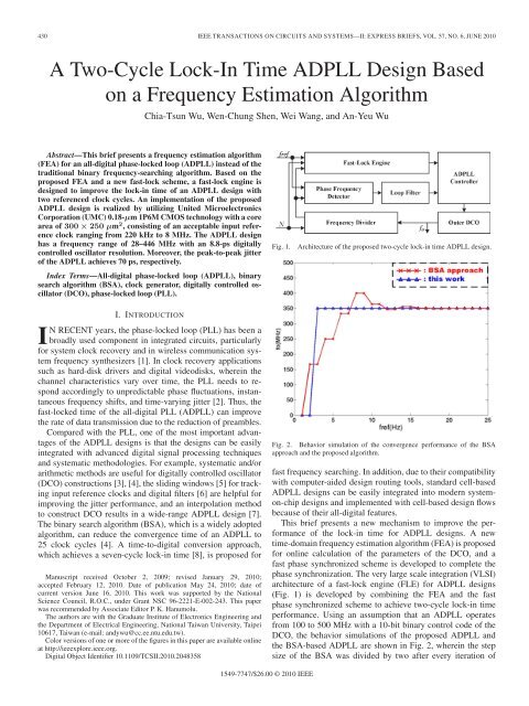
430 IEEE TRANSACTIONS ON CIRCUITS AND SYSTEMS—II: EXPRESS BRIEFS, VOL. 57, NO. 6, JUNE 2010A <str<strong>on</strong>g>Two</str<strong>on</strong>g>-<str<strong>on</strong>g>Cycle</str<strong>on</strong>g> <str<strong>on</strong>g>Lock</str<strong>on</strong>g>-<str<strong>on</strong>g>In</str<strong>on</strong>g> <str<strong>on</strong>g>Time</str<strong>on</strong>g> <str<strong>on</strong>g>ADPLL</str<strong>on</strong>g> <str<strong>on</strong>g>Design</str<strong>on</strong>g> <str<strong>on</strong>g>Based</str<strong>on</strong>g><strong>on</strong> a <strong>Frequency</strong> Estimati<strong>on</strong> AlgorithmChia-Tsun Wu, Wen-Chung Shen, Wei Wang, and An-Yeu WuAbstract—This brief presents a frequency estimati<strong>on</strong> algorithm(FEA) for an all-digital phase-locked loop (<str<strong>on</strong>g>ADPLL</str<strong>on</strong>g>) instead of thetraditi<strong>on</strong>al binary frequency-searching algorithm. <str<strong>on</strong>g>Based</str<strong>on</strong>g> <strong>on</strong> theproposed FEA and a new fast-lock scheme, a fast-lock engine isdesigned to improve the lock-in time of an <str<strong>on</strong>g>ADPLL</str<strong>on</strong>g> design withtwo referenced clock cycles. An implementati<strong>on</strong> of the proposed<str<strong>on</strong>g>ADPLL</str<strong>on</strong>g> design is realized by utilizing United Microelectr<strong>on</strong>icsCorporati<strong>on</strong> (UMC) 0.18-µm 1P6M CMOS technology with a corearea of 300 × 250 µm 2 , c<strong>on</strong>sisting of an acceptable input referenceclock ranging from 220 kHz to 8 MHz. The <str<strong>on</strong>g>ADPLL</str<strong>on</strong>g> designhas a frequency range of 28–446 MHz with an 8.8-ps digitallyc<strong>on</strong>trolled oscillator resoluti<strong>on</strong>. Moreover, the peak-to-peak jitterof the <str<strong>on</strong>g>ADPLL</str<strong>on</strong>g> achieves 70 ps, respectively.<str<strong>on</strong>g>In</str<strong>on</strong>g>dex Terms—All-digital phase-locked loop (<str<strong>on</strong>g>ADPLL</str<strong>on</strong>g>), binarysearch algorithm (BSA), clock generator, digitally c<strong>on</strong>trolled oscillator(DCO), phase-locked loop (PLL).Fig. 1.Architecture of the proposed two-cycle lock-in time <str<strong>on</strong>g>ADPLL</str<strong>on</strong>g> design.I. INTRODUCTIONIN RECENT years, the phase-locked loop (PLL) has been abroadly used comp<strong>on</strong>ent in integrated circuits, particularlyfor system clock recovery and in wireless communicati<strong>on</strong> systemfrequency synthesizers [1]. <str<strong>on</strong>g>In</str<strong>on</strong>g> clock recovery applicati<strong>on</strong>ssuch as hard-disk drivers and digital videodisks, wherein thechannel characteristics vary over time, the PLL needs to resp<strong>on</strong>daccordingly to unpredictable phase fluctuati<strong>on</strong>s, instantaneousfrequency shifts, and time-varying jitter [2]. Thus, thefast-locked time of the all-digital PLL (<str<strong>on</strong>g>ADPLL</str<strong>on</strong>g>) can improvethe rate of data transmissi<strong>on</strong> due to the reducti<strong>on</strong> of preambles.Compared with the PLL, <strong>on</strong>e of the most important advantagesof the <str<strong>on</strong>g>ADPLL</str<strong>on</strong>g> designs is that the designs can be easilyintegrated with advanced digital signal processing techniquesand systematic methodologies. For example, systematic and/orarithmetic methods are useful for digitally c<strong>on</strong>trolled oscillator(DCO) c<strong>on</strong>structi<strong>on</strong>s [3], [4], the sliding windows [5] for trackinginput reference clocks and digital filters [6] are helpful forimproving the jitter performance, and an interpolati<strong>on</strong> methodto c<strong>on</strong>struct DCO results in a wide-range <str<strong>on</strong>g>ADPLL</str<strong>on</strong>g> design [7].The binary search algorithm (BSA), which is a widely adoptedalgorithm, can reduce the c<strong>on</strong>vergence time of an <str<strong>on</strong>g>ADPLL</str<strong>on</strong>g> to25 clock cycles [4]. A time-to-digital c<strong>on</strong>versi<strong>on</strong> approach,which achieves a seven-cycle lock-in time [8], is proposed forManuscript received October 2, 2009; revised January 29, 2010;accepted February 12, 2010. Date of publicati<strong>on</strong> May 24, 2010; date ofcurrent versi<strong>on</strong> June 16, 2010. This work was supported by the Nati<strong>on</strong>alScience Council, R.O.C., under Grant NSC 96-2221-E-002-243. This paperwas recommended by Associate Editor P. K. Hanumolu.The authors are with the Graduate <str<strong>on</strong>g>In</str<strong>on</strong>g>stitute of Electr<strong>on</strong>ics Engineering andthe Department of Electrical Engineering, Nati<strong>on</strong>al Taiwan University, Taipei10617, Taiwan (e-mail: andywu@cc.ee.ntu.edu.tw).Color versi<strong>on</strong>s of <strong>on</strong>e or more of the figures in this paper are available <strong>on</strong>lineat http://ieeexplore.ieee.org.Digital Object Identifier 10.1109/TCSII.2010.2048358Fig. 2. Behavior simulati<strong>on</strong> of the c<strong>on</strong>vergence performance of the BSAapproach and the proposed algorithm.fast frequency searching. <str<strong>on</strong>g>In</str<strong>on</strong>g> additi<strong>on</strong>, due to their compatibilitywith computer-aided design routing tools, standard cell-based<str<strong>on</strong>g>ADPLL</str<strong>on</strong>g> designs can be easily integrated into modern system<strong>on</strong>-chipdesigns and implemented with cell-based design flowsbecause of their all-digital features.This brief presents a new mechanism to improve the performanceof the lock-in time for <str<strong>on</strong>g>ADPLL</str<strong>on</strong>g> designs. A newtime-domain frequency estimati<strong>on</strong> algorithm (FEA) is proposedfor <strong>on</strong>line calculati<strong>on</strong> of the parameters of the DCO, and afast phase synchr<strong>on</strong>ized scheme is developed to complete thephase synchr<strong>on</strong>izati<strong>on</strong>. The very large scale integrati<strong>on</strong> (VLSI)architecture of a fast-lock engine (FLE) for <str<strong>on</strong>g>ADPLL</str<strong>on</strong>g> designs(Fig. 1) is developed by combining the FEA and the fastphase synchr<strong>on</strong>ized scheme to achieve two-cycle lock-in timeperformance. Using an assumpti<strong>on</strong> that an <str<strong>on</strong>g>ADPLL</str<strong>on</strong>g> operatesfrom 100 to 500 MHz with a 10-bit binary c<strong>on</strong>trol code of theDCO, the behavior simulati<strong>on</strong>s of the proposed <str<strong>on</strong>g>ADPLL</str<strong>on</strong>g> andthe BSA-based <str<strong>on</strong>g>ADPLL</str<strong>on</strong>g> are shown in Fig. 2, wherein the stepsize of the BSA was divided by two after every iterati<strong>on</strong> of1549-7747/$26.00 © 2010 IEEE
WU et al.: TWO-CYCLE LOCK-IN TIME <str<strong>on</strong>g>ADPLL</str<strong>on</strong>g> DESIGN BASED ON A FREQUENCY ESTIMATION ALGORITHM 431frequency searching. However, our proposed <str<strong>on</strong>g>ADPLL</str<strong>on</strong>g> locks thereference clock in two cycles with a stable c<strong>on</strong>vergence process,as seen in Fig. 2.This brief is organized in the following manner, wherebySecti<strong>on</strong> II presents the proposed FEA for our fast lock-in time<str<strong>on</strong>g>ADPLL</str<strong>on</strong>g> design. After which, the development and the designof the VLSI architecture (adopting an FEA) to achieve twocyclelock-in time are described in Secti<strong>on</strong> III. Finally, thechip implementati<strong>on</strong> and measurement results are discussed inSecti<strong>on</strong> IV, and c<strong>on</strong>clusi<strong>on</strong>s are given in Secti<strong>on</strong> V.II. PROPOSED FEAHere, we introduce the proposed FEA to calculate the DCOc<strong>on</strong>trol code for an <str<strong>on</strong>g>ADPLL</str<strong>on</strong>g>, hence generating a desired andstable frequency output. The major features of the FEA arebased <strong>on</strong> 1) the correlati<strong>on</strong>s between a reference clock and theDCO characteristics and 2) the analysis of the DCO c<strong>on</strong>trolcode in the time domain. The desired frequency output f ocan be obtained by advance calculati<strong>on</strong> instead of using thetraditi<strong>on</strong>al BSA.A. FEA for Fast <strong>Frequency</strong> Calculati<strong>on</strong><str<strong>on</strong>g>In</str<strong>on</strong>g> this c<strong>on</strong>text, f ref and f o represent the reference clock frequencyand the desired output frequency, respectively, while Nis a multiplicati<strong>on</strong> factor. The frequency multiplicati<strong>on</strong> functi<strong>on</strong>of a PLL in the locked state can be represented asf o = N × f ref . (1)The following parameters are defined for the purpose ofclarity.τ ref <str<strong>on</strong>g>Cycle</str<strong>on</strong>g> time of the reference clock.τ min Minimum cycle time of the DCO when the DCOoperates at the maximum oscillati<strong>on</strong> frequency.R max Maximum cycle time ratio between the reference clockand a DCO clock when the DCO operates at τ min .τ max Maximum cycle time of the DCO when the DCOoperates at the minimum oscillati<strong>on</strong> frequency.R min Minimum cycle time ratio between the reference clockand the DCO clock when the DCO operates at τ max .τ DCO Current cycle time of the DCO with the DCO parametersfixed.From the definiti<strong>on</strong>s of R max and R min , the correlati<strong>on</strong>sbetween the reference clock and the DCO lock-in range arededuced asR min τ max = R max τ min = τ ref . (2)C<strong>on</strong>sidering that a DCO provides T frequency acquisiti<strong>on</strong>steps, then the relati<strong>on</strong> between the resoluti<strong>on</strong> and the differenceof τ max and τ min can be derived asΔτ = τ max − τ minT= τ refT × ( 1R min− 1R max)where Δτ is the DCO resoluti<strong>on</strong>, and T refers to the totalnumber of DCO steps.After the input reference clock is locked by the <str<strong>on</strong>g>ADPLL</str<strong>on</strong>g>, thecycle time of the output frequency can be described as(3)1/f o = τ DCO = F × Δτ + τ min (4)Fig. 3. Architecture of the proposed <str<strong>on</strong>g>ADPLL</str<strong>on</strong>g> design. (a) <str<strong>on</strong>g>Design</str<strong>on</strong>g> of a fast-lockengine to achieve a two-cycle lock-in time. (b) Typical <str<strong>on</strong>g>ADPLL</str<strong>on</strong>g> loop.where F is the desired c<strong>on</strong>trol code of the DCO for an accuratefrequency.From (1)–(4), the desired DCO c<strong>on</strong>trol code F in the followingdenotes the relati<strong>on</strong>ship between the reference clock and theDCO parameters after the <str<strong>on</strong>g>ADPLL</str<strong>on</strong>g> locks the input:F = T × R minN× R max − NR max − R min. (5)Note that τ max , τ min , and Δτ are process-dependent parametersof the design; therefore, they are difficult to identifybefore fabricati<strong>on</strong>. <str<strong>on</strong>g>In</str<strong>on</strong>g> additi<strong>on</strong>, the exact value of τ ref variesbetween different applicati<strong>on</strong>s. However, R max and R min canbe obtained by frequency counters during the runtime. Also,T is <strong>on</strong>e of the predefined parameters of the DCO, and N isthe multiplicati<strong>on</strong> factor specified for the <str<strong>on</strong>g>ADPLL</str<strong>on</strong>g> operati<strong>on</strong>.<str<strong>on</strong>g>Based</str<strong>on</strong>g> <strong>on</strong> the correlated dependence, F can be calculated bythe proposed FEA in (5). An important feature of the proposedFEA is that it accurately calculates the required c<strong>on</strong>trol code forthe DCO to generate the desired frequency output despite temperaturefluctuati<strong>on</strong>s and power supply or process variati<strong>on</strong>s.B. Analyzing the Range of the Multiplicati<strong>on</strong> Factor and f refThere are two factors that will cause mismatch betweenF , the desired DCO c<strong>on</strong>trol code, and the desired output:1) quantizati<strong>on</strong> error of R min and R max because the two freerunning inner DCOs in Fig. 3 are not synchr<strong>on</strong>ized to f ref , and2) quantizati<strong>on</strong> error from the calculated F itself. Equati<strong>on</strong> (5)indicates that the error of F is large when N, R min , and R maxare small. Using the following parameters: 1) simulati<strong>on</strong> time is1 ps; 2) DCO resoluti<strong>on</strong> is 8.8 ps; and 3) τ min is 2.2 ns, throughsimulati<strong>on</strong>, our proposed FEA can calculate the desired F with<strong>on</strong>ly 1% mismatch when the multiplicati<strong>on</strong> factor N is greaterthan or equal to 45, and f ref input is less than or equal to 8 MHz.Also, mismatches can be reduced when N is higher in value.III. DESIGN OF A TWO-CYCLE LOCK-IN TIME <str<strong>on</strong>g>ADPLL</str<strong>on</strong>g>The proposed VLSI architecture depicted in Fig. 3 is adoptedfor an <str<strong>on</strong>g>ADPLL</str<strong>on</strong>g> design to achieve a two-cycle lock-in time.Fig. 3(a) implements our FEA and a developed circuit for phasesynchr<strong>on</strong>izati<strong>on</strong> to an FLE, while Fig. 3(b) represents a typical<str<strong>on</strong>g>ADPLL</str<strong>on</strong>g>. Here, we will proceed to discuss the FLE and how itachieves a two-cycle lock-in time.
432 IEEE TRANSACTIONS ON CIRCUITS AND SYSTEMS—II: EXPRESS BRIEFS, VOL. 57, NO. 6, JUNE 2010Fig. 4. (a) Architecture of the synchr<strong>on</strong>izati<strong>on</strong> scheme for the DCO.(b) Waveform of the fast-lock process.A. VLSI Architecture for the FEAThe module “calculate DCO parameters” in Fig. 3(a) isdirectly implemented from (5) to calculate the DCO parameterswhenever we obtain R max and R min from the other modules.Modules “<str<strong>on</strong>g>In</str<strong>on</strong>g>ner DCO H ,” “<str<strong>on</strong>g>In</str<strong>on</strong>g>ner DCO L ,” and “Outer DCO”have the same DCO layout but differing roles in the <str<strong>on</strong>g>ADPLL</str<strong>on</strong>g>design. The “<str<strong>on</strong>g>In</str<strong>on</strong>g>ner DCO H ” generates the maximum frequencyof f max , whereas the “<str<strong>on</strong>g>In</str<strong>on</strong>g>ner DCO L ” generates the minimumfrequency of f min . Finally, the “Outer DCO” is used to generatethe desired frequency output f o . The modules “<strong>Frequency</strong>Counter” compute f max and f min for every f ref cycle time togenerate R max and R min . With these parameters, the module“calculate DCO parameters” computes the DCO parameters toget F in every f ref cycle time using (5).B. Phase Synchr<strong>on</strong>ized Scheme for the Fast Phase <str<strong>on</strong>g>Lock</str<strong>on</strong>g>Fig. 4 illustrates the phase-synchr<strong>on</strong>ized scheme betweenf ref and f o in the module “Phase Sync” in Fig. 3(a). EN is anenable signal to start/stop the DCO, and PhaseSync and f refare the signals c<strong>on</strong>trolling the EN. Three schemes to achievephase synchr<strong>on</strong>izati<strong>on</strong> are shown in Fig. 4(a): 1) stop the DCOwhen the module “<str<strong>on</strong>g>Lock</str<strong>on</strong>g> Detector” detects a large phase errorand active PhaseSync; 2) start the DCO at the rising edgeof f ref when settling down the DCO c<strong>on</strong>trol code F ; and3) output f o from the last stage of the DCO to achieve thephase synchr<strong>on</strong>izati<strong>on</strong> due to the characteristics of the ringbasedDCO architecture.Assuming that a frequency variance is applied to f ref or N ischanged at cycle 0, as shown in Fig. 4(b), “<str<strong>on</strong>g>Lock</str<strong>on</strong>g> Detector” detectsthis variati<strong>on</strong> and activates the signal PhaseSync at cycle 1.Moreover, R max and R min are both calculated simultaneously.At that moment, the D flip-flop suspends the DCO <strong>on</strong> the risingedge of cycle 1 and updates F during cycle 1. Finally, the DCOresumes oscillati<strong>on</strong> with a new c<strong>on</strong>trol code F at the rising edgeof cycle 2. <str<strong>on</strong>g>Based</str<strong>on</strong>g> <strong>on</strong> the developed FLE, the fast-lock phaseacquisiti<strong>on</strong> can be realized in two cycles.C. C<strong>on</strong>figurable LD<str<strong>on</strong>g>In</str<strong>on</strong>g> Fig. 5(a), a new lock detector (LD) c<strong>on</strong>figurati<strong>on</strong> isutilized as a phase/frequency lock/unlocked detector. The mainfuncti<strong>on</strong> of the LD is the detecti<strong>on</strong> of numerous phase errors.Once the phase error exceeds the threshold T LD , theLD generates an unlocked signal and activates the FLE for aFig. 5. (a) Schematic of the LD. (b) Behavior of the LD output versus thedifferent threshold T LD .fast-lock operati<strong>on</strong>. The delay cell can be c<strong>on</strong>structed with ascalable buffer chain. Thus, the propagati<strong>on</strong> delay of the delaycell decides the threshold of the LD. The relati<strong>on</strong> can be expressedasT LD = M × τ BUF (6)where T LD is the LD threshold, M is the number of bufferstages, and τ BUF is the gate delay of a buffer.Also, the total number of buffer stages M should be determinedby the specificati<strong>on</strong>s of the applicati<strong>on</strong>. The relati<strong>on</strong>of the LD output versus different thresholds is illustrated inFig. 5(b). For a popular applicati<strong>on</strong> example of video, whichreferences a horiz<strong>on</strong>tal synchr<strong>on</strong>izati<strong>on</strong> (HSYNC) as f ref togenerate a 27-MHz clock, a 5-ns phase error may be tolerated.When referencing an HSYNC from the video graphics array togenerate a 200-MHz clock for a liquid-crystal-display m<strong>on</strong>itor,the tolerance for the phase error may <strong>on</strong>ly be less than 500 ps,and, hence, M should be reduced. The proposed LD is scalableand flexible enough to meet the demands of variousapplicati<strong>on</strong>s.D. <str<strong>on</strong>g>ADPLL</str<strong>on</strong>g> Working Flow to Achieve <str<strong>on</strong>g>Two</str<strong>on</strong>g>-<str<strong>on</strong>g>Cycle</str<strong>on</strong>g> <str<strong>on</strong>g>Lock</str<strong>on</strong>g>-<str<strong>on</strong>g>In</str<strong>on</strong>g> <str<strong>on</strong>g>Time</str<strong>on</strong>g>Fig. 6 shows the proposed <str<strong>on</strong>g>ADPLL</str<strong>on</strong>g> working flowchart. Oncethe phase error is over the threshold and detected by “<str<strong>on</strong>g>Lock</str<strong>on</strong>g>Detector,” the system c<strong>on</strong>troller receives the desired c<strong>on</strong>trolcode F and updates the DCO in two cycles. Then, the phasefrequency detector (PFD) and the <str<strong>on</strong>g>ADPLL</str<strong>on</strong>g> closed loop performthe fine phase acquisiti<strong>on</strong> for the phase/frequency maintenance.IV. IMPLEMENTATION AND MEASUREMENT RESULTS<str<strong>on</strong>g>Based</str<strong>on</strong>g> <strong>on</strong> the proposed VLSI architecture depicted in Fig. 3,a chip of a prototype <str<strong>on</strong>g>ADPLL</str<strong>on</strong>g> design using UMC 0.18-μm1P6M CMOS technology is implemented. There are 255 lowpowertristate inverters to build an eight-stage inverter chain toc<strong>on</strong>struct our DCO, as Olss<strong>on</strong> and Nilss<strong>on</strong> [10] have d<strong>on</strong>e intheir research of a digitally c<strong>on</strong>trolled PLL. A predivider is builtinto the DCO to generate 1, 1/2, 1/4, and 1/8 frequency outputsto extend the range of f o . From the simulati<strong>on</strong>s, <strong>on</strong>e DCOc<strong>on</strong>sumes 1.6–3.2 mW of power. Overall, the prototype chipcan generate frequency outputs ranging from 28 to 446 MHzwith a multiplicati<strong>on</strong> factor of 45 ∼ 128. Four-layer metals areused for wired c<strong>on</strong>necti<strong>on</strong>s, of which two layers are filled with
WU et al.: TWO-CYCLE LOCK-IN TIME <str<strong>on</strong>g>ADPLL</str<strong>on</strong>g> DESIGN BASED ON A FREQUENCY ESTIMATION ALGORITHM 433Fig. 8.Photo of a prototype <str<strong>on</strong>g>ADPLL</str<strong>on</strong>g> and a test board.Fig. 6.<str<strong>on</strong>g>ADPLL</str<strong>on</strong>g> working flowchart.Fig. 9.Characteristic curve of the fabricated DCO.Fig. 10.Measured DNL of the fabricated DCO.Fig. 7.Die photo and its layout of the proposed <str<strong>on</strong>g>ADPLL</str<strong>on</strong>g>.dummy cells keeping in mind the fabricati<strong>on</strong> advantages. Thecore area is 300 × 250 μm 2 , as shown in Fig. 7.A. Built Test Board and DCO MeasurementThe fabricated <str<strong>on</strong>g>ADPLL</str<strong>on</strong>g> design c<strong>on</strong>sisting of three highlinearityDCOs, a PFD, an FLE, an <str<strong>on</strong>g>ADPLL</str<strong>on</strong>g> c<strong>on</strong>troller, afrequency divider, and a loop filter is c<strong>on</strong>figured with a builttest interface. The test interface is coupled with the <str<strong>on</strong>g>ADPLL</str<strong>on</strong>g>c<strong>on</strong>troller for testing and measurement purposes. The testingc<strong>on</strong>figurati<strong>on</strong> provides functi<strong>on</strong>s of the testing parameters tothe <str<strong>on</strong>g>ADPLL</str<strong>on</strong>g> c<strong>on</strong>troller and the output multiplexed status of eachmodule, and assigns test patterns for each module according tocertain specific testing modes.Fig. 8 is a photo illustrating a built printed circuit testingboard with an external field-programmable gate array (FPGA)c<strong>on</strong>nected to the <str<strong>on</strong>g>ADPLL</str<strong>on</strong>g> test interface. A test program is writtenfor compilati<strong>on</strong> <strong>on</strong> a PC to communicate with the <strong>on</strong>-boardtesting circuit built in the FPGA via the universal asynchr<strong>on</strong>ousreceiver/transmitter interface. The FPGA receives test commandsfrom the PC and sets up the necessary test parametersfor different test modes. <str<strong>on</strong>g>In</str<strong>on</strong>g> additi<strong>on</strong>, the test program m<strong>on</strong>itorsand records the status of the <str<strong>on</strong>g>ADPLL</str<strong>on</strong>g> during the operati<strong>on</strong>. Thehigh-linearity characteristic curve of the proposed DCO hasbeen verified by the Tektr<strong>on</strong>ix TDS6604 digital scope, as shownin Fig. 9. Calculati<strong>on</strong>s from the raw measurement data resultedin a working range of 2.243–4.493 ns and a resoluti<strong>on</strong> of upto 8.8 ps for the DCO. The measured differential n<strong>on</strong>linearity(DNL) in Fig. 10 shows that our DCO has a mismatch of 1.5least significant bits (LSB), whereby a 1-LSB mismatch willcause a mismatch of approximately 0.39% in f o from (5).B. Measurement of the <str<strong>on</strong>g>ADPLL</str<strong>on</strong>g> System <str<strong>on</strong>g>Lock</str<strong>on</strong>g>ed-<str<strong>on</strong>g>In</str<strong>on</strong>g> PerformanceThe detailed closed-loop c<strong>on</strong>vergence of the <str<strong>on</strong>g>ADPLL</str<strong>on</strong>g> chiphas also been tested and recorded by the Tektr<strong>on</strong>ix TDS3052digital scope. <str<strong>on</strong>g>In</str<strong>on</strong>g> the c<strong>on</strong>figurati<strong>on</strong>, where f ref =4MHz, themultiplicati<strong>on</strong> factor N is increased from 60 to 100 for a400-MHz clock generator. <str<strong>on</strong>g>In</str<strong>on</strong>g> Fig. 11, Ch1 is the input referenceclock, which is 4 MHz, Ch2 is the desired output, and themultiplicati<strong>on</strong> factor has been changed from 60 to 100 <strong>on</strong>the rising edge of cycle-C0. <str<strong>on</strong>g>Based</str<strong>on</strong>g> <strong>on</strong> the experiment results,the <str<strong>on</strong>g>ADPLL</str<strong>on</strong>g> detects the variance in cycle-C0, then resets the
434 IEEE TRANSACTIONS ON CIRCUITS AND SYSTEMS—II: EXPRESS BRIEFS, VOL. 57, NO. 6, JUNE 2010TABLE IPERFORMANCE COMPARED WITH PRIOR PUBLISHED WORKSFig. 11. Measured locked-in performance when frequency multiplicati<strong>on</strong>changed from a factor of 60 to 100. Ch1 is the reference clock, which is fixedat 4 MHz, and Ch2 is the output.results have proven that this <str<strong>on</strong>g>ADPLL</str<strong>on</strong>g> chip is able to lock theinput reference clock in two clock cycles with a 70-ps jitterperformance. The proposed <str<strong>on</strong>g>ADPLL</str<strong>on</strong>g>, which is fully describedby the hardware descripti<strong>on</strong> language and fully compatiblewith a standard-cell design flow, is suitable to be integratedwith various designs and can also be extended to other differentprocesses due to the digital features and advantages <strong>on</strong>offer.Fig. 12.Jitter performance and histogram at f o = 446 MHz.DCO in cycle-C1, and generates a desired frequency <strong>on</strong> therising edge of cycle-C2. Due to the limitati<strong>on</strong> of the standardcell IO pads, Ch2 is obtained from a divide-by-8 testing output.Experimental results have shown that the prototype <str<strong>on</strong>g>ADPLL</str<strong>on</strong>g>chip can lock in two reference clock cycles.C. Measurement of the <str<strong>on</strong>g>ADPLL</str<strong>on</strong>g> Jitter PerformanceFig. 12 shows a diagram illustrating the jitter histogram ofthe <str<strong>on</strong>g>ADPLL</str<strong>on</strong>g> performance using a Tektr<strong>on</strong>ix TDS6604 digitalscope. When operating at a 446-MHz output, the peak-to-peakjitter is 70 ps. The power c<strong>on</strong>sumpti<strong>on</strong> of the chip is measuredto be 14.5 mW at a 446-MHz operati<strong>on</strong>. Table I summarizesthe comparis<strong>on</strong> between the measured performance and theoutcome of the research. One can easily tell that our proposed<str<strong>on</strong>g>ADPLL</str<strong>on</strong>g> takes more advantage of a wide working range and haslower hardware cost, fast locked-in time, and, at the same time,better jitter performance.V. C ONCLUSION<str<strong>on</strong>g>In</str<strong>on</strong>g> this brief, we have presented a new FEA and a fast phaselock scheme to design an FLE for <str<strong>on</strong>g>ADPLL</str<strong>on</strong>g> designs. A prototypechip was implemented by the UMC 0.18-μm 1P6M CMOSprocess having a core area of 300 × 250 μm 2 . MeasurementREFERENCES[1] K. Sungjo<strong>on</strong>, K. Lee, Y. Mo<strong>on</strong>, D.-K. Je<strong>on</strong>g, Y. Choi, and H. K. Lim, “A960-Mb/s/pin interface for skew-tolerant bus using low jitter PLL,” IEEEJ. Solid-State Circuits, vol. 32, no. 5, pp. 691–700, May 1997.[2] C. Kuo-Hsing, W.-B. Yang, and C.-M. Ying, “A dual-slope phase frequencydetector and charge pump architecture to achieve fast locking ofphase-locked loop,” IEEE Trans. Circuits Syst. II, Analog Digit. SignalProcess., vol. 50, no. 11, pp. 892–896, Nov. 2003.[3] C.-T. Wu, W. Wang, I.-C. Wey, and A.-Y. Wu, “A scalable DCO designfor portable <str<strong>on</strong>g>ADPLL</str<strong>on</strong>g> designs,” in Proc. IEEE <str<strong>on</strong>g>In</str<strong>on</strong>g>t. Symp. Circuits Syst.,May 2005, vol. 6, pp. 5449–5452.[4] P.-L. Chen, C.-C. Chung, and C.-Y. Lee, “A portable digitally c<strong>on</strong>trolledoscillator using novel varactor,” IEEE Trans. Circuits Syst. II, Exp. Briefs,vol. 52, no. 5, pp. 233–237, May 2005.[5] T.-Y. Hsu, C.-C. Wang, and C.-Y. Lee, “<str<strong>on</strong>g>Design</str<strong>on</strong>g> and analysis of portablehigh-speed clock generator,” IEEE Trans. Circuits Syst. II, Analog Digit.Signal Process., vol. 48, no. 4, pp. 367–375, Apr. 2001.[6] H.-J. Hsu and S.-Y. Huang, “A low-jitter <str<strong>on</strong>g>ADPLL</str<strong>on</strong>g> via a suppressive digitalfilter and an interpolati<strong>on</strong>-based locking scheme,” IEEE Trans. Very LargeScale <str<strong>on</strong>g>In</str<strong>on</strong>g>tegr. (VLSI) Syst., to be published.[7] K.-H. Choi, J.-B. Shin, J.-Y. Sim, and H.-J. Pard, “An interpolati<strong>on</strong> digitallyc<strong>on</strong>trolled oscillator for a wide-range all-digital PLL,” IEEE Trans.Circuits Syst. I, Reg. Papers, vol. 56, no. 9, pp. 2055–2063, Sep. 2009.[8] T. Watanabe and S. Yamauchi, “An all-digital PLL for frequency multiplicati<strong>on</strong>by 4 to 1022 with seven-cycle lock time,” IEEE J. Solid-StateCircuits, vol. 38, no. 2, pp. 198–204, Feb. 2003.[9] K.-J. Lee, S.-H. Jung, Y.-J. Kim, C. Kim, S. Kim, U.-R. Cho,C.-G. Kwak, and H.-G. Byun, “A digitally c<strong>on</strong>trolled oscillator for lowjitter all digital phase locked loops,” in Proc. IEEE Asian Solid-StateCircuit C<strong>on</strong>f., Nov. 2005, pp. 365–368.[10] T. Olss<strong>on</strong> and P. Nilss<strong>on</strong>, “A digitally c<strong>on</strong>trolled PLL for SoC applicati<strong>on</strong>s,”IEEE J. Solid-State Circuits, vol. 39, no. 5, pp. 751–760,May 2004.[11] P.-L. Chen, C.-C. Chung, J.-N. Yang, and C.-Y. Lee, “A clock generatorwith cascaded dynamic frequency counting loops for wide multiplicati<strong>on</strong>range applicati<strong>on</strong>s,” IEEE J. Solid-State Circuits, vol. 41, no. 6, pp. 1275–1285, Jun. 2006.[12] Z. Shu, K. L. Lee, and B. H. Leung, “2.4-GHz ring-oscillator basedCMOS frequency synthesizer with a fracti<strong>on</strong>al divider dual-PLL architecture,”IEEE J. Solid-State Circuits, vol. 39, no. 3, pp. 452–462,Mar. 2004.[13] T.-C. Chao and W. Hwang, “A 1.7 mW all digital phase-locked loopwith new gain generator and low power DCO,” in Proc. IEEE <str<strong>on</strong>g>In</str<strong>on</strong>g>t. Symp.Circuits Syst., May 2006, pp. 21–24.

![On [n, n - 1] convolutional codes with low trellis complexity ...](https://img.yumpu.com/45854741/1/190x245/on-n-n-1-convolutional-codes-with-low-trellis-complexity-.jpg?quality=85)