Todd Christopher Bailey - Willson Research Group - The University ...
Todd Christopher Bailey - Willson Research Group - The University ...
Todd Christopher Bailey - Willson Research Group - The University ...
You also want an ePaper? Increase the reach of your titles
YUMPU automatically turns print PDFs into web optimized ePapers that Google loves.
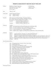
<strong>Todd</strong> <strong>Christopher</strong> <strong>Bailey</strong> 11160 Jollyville Road #434 · Austin, TX 78759512.795.8985 · bailey@che.utexas.eduObjectiveEducation<strong>Research</strong>Experience<strong>Research</strong> or development position in a dynamic and challenging environment withopportunities for professional and personal growth.<strong>The</strong> <strong>University</strong> of Texas, Austin, TX. Doctoral Candidate in Chemical Engineering;Ph.D. expected in February 2003. GPA 3.5/4.0Massachusetts Institute of Technology, Cambridge, MA. S.B., Chemical Engineering,June 1998. GPA 4.4/5.0.Hudson Valley Community College, Troy, NY. A.S. Engineering Science, May 1996.GPA 3.9/4.0<strong>The</strong> <strong>University</strong> of Texas at Austin. August 1998 – present. Advised by J.G. Ekerdt andC.G. <strong>Willson</strong>. Contributed to various aspects of Step and Flash Imprint Lithography(SFIL), a new, low-cost lithography technology that enables patterning at smallerdimensions than current optical projection lithographic techniques.Massachusetts Institute of Technology. January 1997 – June 1998. Advised by K.K.Gleason. Undergraduate research on pulsed plasma-enhanced chemical vapor depositionof fluoropolymers.Motorola Physical Sciences <strong>Research</strong> Labs, Tempe, AZ. May-August 2001. Graduatestudent intern in the Advanced Lithography group. Developed baseline processes forimprint template fabrication for use in Step and Flash Imprint Lithography.Philips Analytical, Natick, MA. June – October 1999. Graduate student intern assignedto serve as liaison with Sematech Interconnect <strong>Group</strong> during development of a tool thatuses impulsive stimulated thermal scattering technology. Interfaced daily with Sematechstaff and assignees to determine tool needs, and worked with Philips staff in MA todemonstrate tool capabilities.Advanced Micro Devices Submicron Development Center, Sunnyvale, CA. June -August 1998. Summer Intern in the Advanced Process Development Diffusion group.Developed a factorial DOE to map parameter space for a new RTP cluster tool.Experimented with various Si 3 N 4 and SiO 2 recipes, and dielectric stacks, and comparedthem to standard LPCVD films.Intel Corporation, Beaverton, OR. June - August 1997. Summer Intern, Tungsten CVDgroup. Created an on-line defect picture book for use within the fab. Helped isolateparticle-producing areas within the tools, and developed a troubleshooting system fordefects. Analyzed etch endpoint data to revise a process recipe.Cambridge Partnership for Public Education, Cambridge, MA. November 1996 -January 1998. Technology Trainer. Co-authored a training and certification program incomputer and related technologies to be used by teachers in the Cambridge Public Schoolsystem. Gave lessons in basic computing to members of the local community.Chi Chi's Mexican Restaurant, Albany, NY. August 1989 - February 1993. GeneralManager. Responsible for a $2.0M operating budget. Supervised 5 managers and inexcess of 100 employees. Developed and executed plan to build revenues and lowerfood/liquor/labor costs from 89% to 77%, which helped bring the restaurant intoprofitability.Publications T.C. <strong>Bailey</strong>, J.G. Ekerdt, and C.G. <strong>Willson</strong>, “Film Thickness Variation Implications onDefect Inspection for Imprint Lithography,” J. Microlith, Microfab, & Microsystems,(2002) submitted for publication.T.C. <strong>Bailey</strong>, et al., “Step and Flash Imprint Lithography: A Low-Pressure, Room
Temperature Nanoimprint Patterning Process”, in Alternative Lithography. Unleashingthe Potentials of Nanotechnology, C.S. Torres, Editor. 2003, Elsevier.T.C. <strong>Bailey</strong>, et al.; “Recent Advances in Step and Flash Imprint Lithography;” Proc.Arch Interface (2002).T.C. <strong>Bailey</strong>, et al.; “Step and Flash Imprint Lithography: An Efficient Nanoscale PrintingTechnology;” J. Photopolymer Sci. Tech. 15(3) (2002), p.481.W.J. Dauksher, et al.; “Characterization of and Imprint Results using ITO-based Step andFlash Imprint Lithography Templates;” J. Vac. Sci. Tech. B 20 (6) (2002), p.2857.D.J. Resnick, et al.; “High Resolution Templates for Step and Flash ImprintLithography;” Proc. SPIE: Emerging Lithographic Technologies VI, v.4688 (2002) ,p.2896.T.C. <strong>Bailey</strong>, et al.; “Template Fabrication Schemes for Step and Flash ImprintLithography”; Microelectronic Engineering v.61-62 (2002), p. 461.M. Colburn, et al.; “Development and Advantages of Step-and-Flash Lithography”; SolidState Technology; 46 (7) (2001); p. 67.T. <strong>Bailey</strong>, et al.; “Step and Flash Imprint Lithography: Defect Analysis”; J. Vac. Sci.Tech. B 19(6) (2001), p. 2806.T. <strong>Bailey</strong>, et al.; “Step and Flash Imprint Lithography: Template Surface Treatment andDefect Analysis”; J. Vac. Sci. Tech. B 18(6) (2000), p. 3572.M. Gostein, et al.. "Thickness measurement for Cu and Ta thin films usingoptoacoustics." Proceedings of the IEEE IITC, 2000. Burlingame / San Francisco, CA.(2000) p. 176.T. <strong>Bailey</strong>; Pulsed Plasma-Enhanced Chemical Vapor Deposition of Poly-Para-XylyleneFilms from [2,2]Paracyclophane, and <strong>The</strong> Effect of Pulsing Parameters and Peak PowerInput on Pulsed Plasma-Enhanced Chemical Vapor Deposited Fluorocarbon Films fromHexafluoropropylene Oxide; Bachelor <strong>The</strong>sis, Massachusetts Institute of Technology,1998.Patents US Patent Applications 20020093122, 20020094496, 20020115002World Patent Applications WO2002010721, WO2002006902, WO2002008835Honors/ActivitiesZ.D. Bonner Fellow (2000-2003)Member, Sigma Xi, <strong>The</strong> Scientific <strong>Research</strong> Society, MIT chapter (1998-present)Chair, Chemical Engineering Graduate Student Executive Committee (UT 1999-2000)<strong>University</strong> of Texas College of Engineering Thrust Fellow (1998-1999)AIChE Vice President (MIT 1997-1998)HVCC Honors Convocation Guest Speaker (1997)President's Award for Community Service (HVCC 1996)Student Senate President (HVCC 1995-1996)Faculty-Student Association Board member (HVCC 1995-1996)Founder and President, Engineering Science Association (HVCC 1994-1995).


