Design and Implementation of On-board Electrical Power ... - OUFTI-1
Design and Implementation of On-board Electrical Power ... - OUFTI-1
Design and Implementation of On-board Electrical Power ... - OUFTI-1
You also want an ePaper? Increase the reach of your titles
YUMPU automatically turns print PDFs into web optimized ePapers that Google loves.
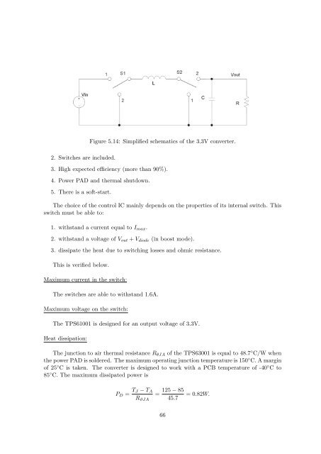
Figure 5.14: Simplified schematics <strong>of</strong> the 3.3V converter.2. Switches are included.3. High expected efficiency (more than 90%).4. <strong>Power</strong> PAD <strong>and</strong> thermal shutdown.5. There is a s<strong>of</strong>t-start.The choice <strong>of</strong> the control IC mainly depends on the properties <strong>of</strong> its internal switch. Thisswitch must be able to:1. withst<strong>and</strong> a current equal to I max .2. withst<strong>and</strong> a voltage <strong>of</strong> V out + V diode (in boost mode).3. dissipate the heat due to switching losses <strong>and</strong> ohmic resistance.This is verified below.Maximum current in the switch:The switches are able to withst<strong>and</strong> 1.6A.Maximum voltage on the switch:The TPS61001 is designed for an output voltage <strong>of</strong> 3.3V.Heat dissipation:The junction to air thermal resistance R θJA <strong>of</strong> the TPS63001 is equal to 48.7 ◦ C/W whenthe power PAD is soldered. The maximum operating junction temperature is 150 ◦ C. A margin<strong>of</strong> 25 ◦ C is taken. The converter is designed to work with a PCB temperature <strong>of</strong> -40 ◦ C to85 ◦ C. The maximum dissipated power isP D = T J − T A 125 − 85= = 0.82W.R ϑJA 45.766


