Design and Implementation of On-board Electrical Power ... - OUFTI-1
Design and Implementation of On-board Electrical Power ... - OUFTI-1 Design and Implementation of On-board Electrical Power ... - OUFTI-1
• Output voltage: 5V.• Maximum output current: 200mA.The output voltage is higher than the input voltage. A boost converter will be used.Choice control ICThe LTC3528 from Linear Technology was chosen for the control IC. The devices includesthe control and the switch. There is no need of external rectifier diode (an internal FET takethe place of the diode).The advantages of the LTC3528 model are:1. Very small size.2. High expected efficiency (90% to 95%).3. A special mode improves efficiency at light load.4. Power PAD and thermal shutdown.5. There is a soft-start.6. Low start-up voltage (700mV).The choice of the control IC mainly depends on the properties of its internal switch. Thisswitch must be able to:1. withstand a current equal to I max .2. withstand a voltage of V out + V diode .3. dissipate the heat due to switching losses and ohmic resistance.This is verified below.Maximum current in the switchThe switch is able to withstand 1A.Maximum voltage on the switch:The LTC3528 can be used for an output voltage from 1.6V to 5.25V.Heat dissipation:62
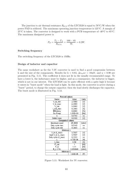
The junction to air thermal resistance R θJA of the LTC3528 is equal to 76 ◦ C/W when thepower PAD is soldered. The maximum operating junction temperature is 125 ◦ C. A margin of25 ◦ C is taken. The converter is designed to work with a PCB temperature of -40 ◦ C to 85 ◦ C.The maximum dissipated power isP D = T J − T A 100 − 85= = 0.2W.R ϑJA 76Switching frequencyThe switching frequency of the LTC3528 is 1MHz.Design of inductor and capacitorThe same worksheet as for the 7.2V converter is used to find a good compromise betweenk and the size of the components. Results for k = 0.84, ∆v m ax = 10mV, and η = 0.90 arepresented in Fig. 5.11. The coefficient k does not lie in the usually recommended range. Tohave a lower k, the inductance must be higher, and as a consequence, the inductor is bigger,which is not in our interest. The LTC3528 can be quite efficient with a quite high k becauseit enters in ”burst mode” when the load is light. In this mode, the converter is active during a”burst” period, to charge the output capacitor; then the load slowly discharges the capacitor.The burst mode is illustrated in Fig. 5.12.Figure 5.11: Worksheet for 5V converter.63
- Page 12 and 13: Chapter 2Requirements of the EPS2.1
- Page 14 and 15: • The Single-Event Upset (SEU)Thi
- Page 16 and 17: the P-POD. RBF pins must fit within
- Page 18 and 19: Figure 2.6: Top view of the PC104 c
- Page 20 and 21: Chapter 3Design of EPS architecture
- Page 22 and 23: • Voltage (4) and current (5) at
- Page 24 and 25: Figure 3.6: The equivalent circuit
- Page 26 and 27: of our Lithium-Polymer batteries va
- Page 28 and 29: Figure 3.12: I-V curve of a solar p
- Page 30 and 31: 3.3.3 CapacityA important value to
- Page 32 and 33: Parameter SLPB723870H4 SLPB554374HN
- Page 34 and 35: of the batteries is kept between -2
- Page 36 and 37: Over Charge Prohibition 4.275 ± 0.
- Page 38 and 39: supplied in 5V. The circuit will be
- Page 40 and 41: Chapter 4The Power Budget4.1 Introd
- Page 42 and 43: Figure 4.1: P-V curve of a solar pa
- Page 44 and 45: 4.3.2 Efficiency of convertersTo at
- Page 46 and 47: Figure 4.3: Consumptions in % in me
- Page 48 and 49: Chapter 5Electrical Design of EPS5.
- Page 50 and 51: V outV in= D. (5.1)Since D ≤ 1, t
- Page 52 and 53: The power losses in the inductor ar
- Page 54 and 55: ∆i L,1 + ∆i L,2 = 0, (5.16)V in
- Page 56 and 57: Using the value of ∆i L given by
- Page 58 and 59: There is no data about the case to
- Page 60 and 61: Capacitor selectionFour 10µF ceram
- Page 64 and 65: Figure 5.12: Burst mode operation (
- Page 66 and 67: Figure 5.14: Simplified schematics
- Page 68 and 69: Figure 5.15: Worksheet for 3.3V con
- Page 70 and 71: sequently, the k was chosen above 0
- Page 72 and 73: where G 1 is the initial control-to
- Page 74 and 75: Figure 5.21: Measured Bode diagram
- Page 76 and 77: Figure 5.26: Equivalence between th
- Page 78 and 79: C f =12πf f R 0f,L f = R 2 0f C f
- Page 80 and 81: Figure 5.37: Schematics of the firs
- Page 82 and 83: R KR >1.45V100mA − 1.3A35= 23.07
- Page 84 and 85: The schematics is shown on figure 5
- Page 86 and 87: A commercial model meets all requir
- Page 88 and 89: Figure 5.45: Schematics of the heat
- Page 90 and 91: PrefixX7X5Y5Z5SuffixTemperature ran
- Page 92 and 93: 6.2.1 The second dissipation system
- Page 94 and 95: • The antenna deployment system.
- Page 96 and 97: 6.3.3 TestsThe engineering model of
- Page 98 and 99: 7.3 ActivitiesAs OUFTI-1 is designe
- Page 100 and 101: 8.1.2 DesignA model of Li-Po batter
- Page 102 and 103: [15] Fabien Jordan, Phase B Electri
- Page 104 and 105: TaK = 273 + TaC;%Photo-current ther
- Page 106 and 107: Appendix BPower budget worksheetIn
- Page 108 and 109: 108
- Page 110 and 111: Appendix CPictures of the prototype
The junction to air thermal resistance R θJA <strong>of</strong> the LTC3528 is equal to 76 ◦ C/W when thepower PAD is soldered. The maximum operating junction temperature is 125 ◦ C. A margin <strong>of</strong>25 ◦ C is taken. The converter is designed to work with a PCB temperature <strong>of</strong> -40 ◦ C to 85 ◦ C.The maximum dissipated power isP D = T J − T A 100 − 85= = 0.2W.R ϑJA 76Switching frequencyThe switching frequency <strong>of</strong> the LTC3528 is 1MHz.<strong>Design</strong> <strong>of</strong> inductor <strong>and</strong> capacitorThe same worksheet as for the 7.2V converter is used to find a good compromise betweenk <strong>and</strong> the size <strong>of</strong> the components. Results for k = 0.84, ∆v m ax = 10mV, <strong>and</strong> η = 0.90 arepresented in Fig. 5.11. The coefficient k does not lie in the usually recommended range. Tohave a lower k, the inductance must be higher, <strong>and</strong> as a consequence, the inductor is bigger,which is not in our interest. The LTC3528 can be quite efficient with a quite high k becauseit enters in ”burst mode” when the load is light. In this mode, the converter is active during a”burst” period, to charge the output capacitor; then the load slowly discharges the capacitor.The burst mode is illustrated in Fig. 5.12.Figure 5.11: Worksheet for 5V converter.63


