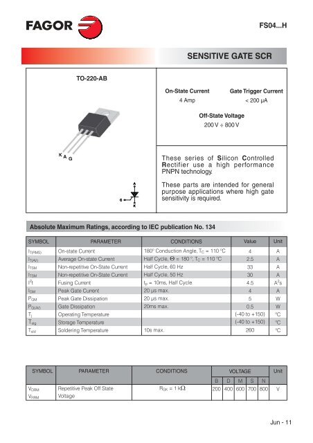
SENSITIVE GATE SCR
SENSITIVE GATE SCR
SENSITIVE GATE SCR

You also want an ePaper? Increase the reach of your titles
YUMPU automatically turns print PDFs into web optimized ePapers that Google loves.
FS04...H<strong>SENSITIVE</strong> <strong>GATE</strong> <strong>SCR</strong>TO-220-ABOn-State Current4 AmpGate Trigger Current< 200 µAOff-State Voltage200 V ÷ 800 VK A GThese series of Silicon ControlledRectifier use a high performancePNPN technology.These parts are intended for generalpurpose applications where high gatesensitivity is required.Absolute Maximum Ratings, according to IEC publication No. 134SYMBOLPARAMETER CONDITIONS Value UnitI T(RMS)I T(AV)I TSMI TSMI 2 tI GMP GMP G(AV)T jT stgT sldOn-state CurrentAverage On-state CurrentNon-repetitive On-State CurrentNon-repetitive On-State CurrentFusing CurrentPeak Gate CurrentPeak Gate DissipationGate DissipationOperating TemperatureStorage TemperatureSoldering Temperature180º Conduction Angle, T C = 110 ºCHalf Cycle, Q = 180 º, T C = 110 ºCHalf Cycle, 60 HzHalf Cycle, 50 Hzt p = 10ms, Half Cycle20 µs max.20 µs max.20ms max.10s max.42.533304.5450.5(-40 to +150)(-40 to +150)260AAAAA 2 sAWWºCºCºCR GK = 1 kW VSYMBOLPARAMETER CONDITIONS VOLTAGE UnitV DRM Repetitive Peak Off StateB200D400M600S700N800V RRM VoltageJun - 11
FS04...H<strong>SENSITIVE</strong> <strong>GATE</strong> <strong>SCR</strong>Electrical CharacteristicsSYMBOLPARAMETER CONDITIONS SENSITIVITY UnitV D = 12 V DC , R L = 140W. T j = 25 °CI GT Gate Trigger CurrentMIN 1 0 15I DRM / I RRM Off-State Leakage Current V D = V DRM , R GK = 1kW T j = 125 °C MAX1mAMAX 20 200 50 µ AV GT Gate Trigger Voltage V D = 12 V DC , R L = 140W, T j = 25 °C MAX0.8VV GD Gate Non Trigger Voltage V D = V DRM , R L = 3.3kW, R GK = 220W MIN0.1VT j = 125 °CV RGM Reverse Gate Voltage I RG = 10µA,MIN8VI H Holding CurrentI T = 500 mA,MAX 5mAI L Latching Current I G = 1.2 I GT MAX6mAdV / dt Critical Rate of Voltage Rise V D = 0.67 x V DRM , R GK =1 kW, MIN 10 5 15 V/µsT j = 125 °CdI / dt Critical Rate of Current Rise I G = 2 x I GT tr £ 100 ns, f = 60 Hz, MIN50A/µsT j = 125 °CV TM On-state Voltageat I T = 8 Amp, tp = 380 µs, T j = 25 °C MAX1.6 VV t (0) Threshold Voltage T j = 125 °CMAX 0.85 Vr d Dynamic resistance T j = 125 °CMAX 46 mWV R = V RRM ,T j = 25 °C MAX5µAR th(j-c)Thermal ResistanceJunction-Amb for DCfor AC 360° conduction angle01022.004ºC/WR th(j-a)Thermal ResistanceJunction-Amb for DCS = 1cm 260°C/WPART NUMBER INFORMATIONF S 04 02 B H 00TUFAGOR<strong>SCR</strong>CURRENTPACKAGINGFORMINGCASEVOLTAGESENSITIVITYJun - 11
FS04...H<strong>SENSITIVE</strong> <strong>GATE</strong> <strong>SCR</strong>Fig. 1: Maximum average power dissipationversus average on-state current.Fig. 2: Average and D.C. on-state currentversus case temperature.P (W)55I T(av) (A)44D.C.3232a = 180 º1360 º100 1 2 3 4 5 6 7aI T(av) (A)00 25 50 75 100 125T case (ºC)Fig. 3: Relative variation of thermal impedancejunction to case versus pulse duration.K = [Z th(j-c) / R th (j-c) ]1.00.50.20.1tp (s)1E+0Fig. 5: Relative variation of holding currentversus gate-cathode resistance (typicalvalues).Fig. 4: Relative variation of gate triggercurrent, holding and latching currentversus junction temperature.I GT , I H (T j ) / I GT , I H (T j = 25 ºC)2.01.81.6 I GT1.41.2I H & I1.0 L0.80.60.40.20.0T j (ºC)-40 -20 0 20 40 60 80 100 120 140Fig. 6: Relative variation of dV/dt immunityversus gate-cathode resistance (typical values).5I H [R GK ] / I H [R GK = 1kW] dV/dt [R GK ] / dV/dt [R GK = 220W]10.00T j = 25 °CT j = 125 °CVD = 0.67xV DRM431.0020.101R GK = (kW)01E-2 1E-1 1E+0 1E-1R GK = (kW)0.010 0.2 0.4 0.6 0.8 1.0 1.2 1.4 1.6 1.8 2.0Jun - 11
FS04...H<strong>SENSITIVE</strong> <strong>GATE</strong> <strong>SCR</strong>Fig. 7: Relative variation of dV/dt immunityversus gate-cathode resistance (typicalvalues).dV/dt [Cgk] / dV/dt [RGK = 220W]I TSM (A)1010 40VD = 0.67 x V DRMT j = 125 ºC35R GK = 220W830Fig. 8: Non repetitive surge peak on-statecurrent versus number of cycles.642Cgk(nF)00 2 4 6 8 10 12 14 16 18 20 22252015105Number of0cycles1 10 100 1000Fig. 9: Non repetitive surge peak on-statecurrent for a sinusoidal pulse with width:tp < 10 ms, and corresponding value of I 2 t.3010I TSM (A). I 2 t (A 2 s)50I TSM T j initial = 25 ºCFig. 10: On-state characteristics (maximumvalues).10I TM (A)T j maxV T(O) = 0.85 Vr d = 90mWT j =T j max5I 2 t1T j 25 ºC21tp(ms)1 2 5 100.10 0.5 1 1.5 2 2.5 3 3.5 4V TM (V)Jun - 11
FS04...H<strong>SENSITIVE</strong> <strong>GATE</strong> <strong>SCR</strong>PACKAGE MECHANICAL DATATO-220ABDøPQD1b2beEe1L1LA1A2ACH1REF.AA1A2bb2cDD1Eee1H1LL1PQDIMENSIONSMilimetersMin. Max.4.471.172.520.711.170.3114.658.5010.012.514.986.1513.403.563.7352.594.671.372.820.911.370.5315.358.9010.362.575.186.4513.963.963.9352.89Mounting Torque1 N.m(*) Limiting values and life support applications, see Web page.Jun - 11