Full 3D Statistical Simulation of Line Edge Roughness in sub-100nm ...
Full 3D Statistical Simulation of Line Edge Roughness in sub-100nm ...
Full 3D Statistical Simulation of Line Edge Roughness in sub-100nm ...

Create successful ePaper yourself
Turn your PDF publications into a flip-book with our unique Google optimized e-Paper software.
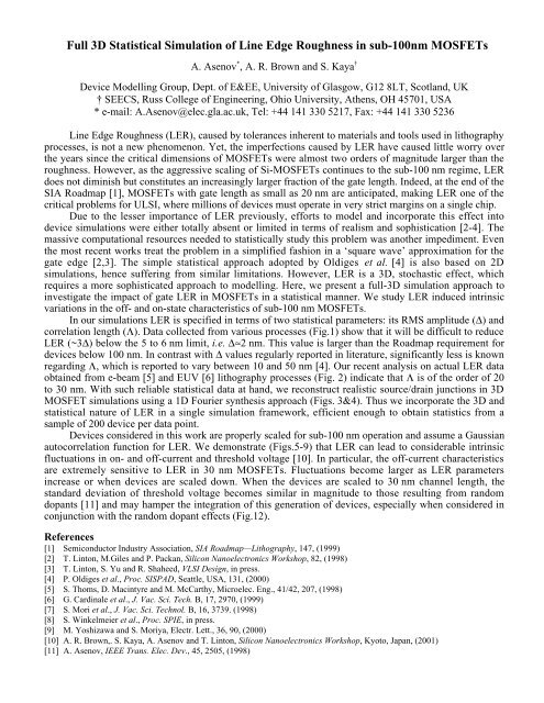
LER (3∆) [nm]151050ASET (i-l<strong>in</strong>e)IBM (i-l<strong>in</strong>e)IMEC (i-l<strong>in</strong>e)SANDIA (EUV)SONY (e-beam)SIA Roadmap (1999)50 100 150 200<strong>L<strong>in</strong>e</strong> Width [nm]Fig.1: Actual data from various advanced lithographyprocesses reported by different labs [4-9] show that LERdoes not scale with l<strong>in</strong>e width and exceeds Roadmaprequirements below 100 nm.Autocorrelation0.80.60.40.20DetectedΛ G=29.3 nmΛ E=25.3 nmOrig<strong>in</strong>al<strong>Edge</strong> Detected0 25 50 75 100 125Distance [nm]Fig. 2: Autocorrelation <strong>of</strong> LER captured from 100 nm EUVl<strong>in</strong>es [6]. Correlation lengths obta<strong>in</strong>ed from Gaussian (Λ G ) andexponential (Λ E ) fits to raw data extracted from edges detection<strong>of</strong> the orig<strong>in</strong>al SEM micrograph.S(q) [arb.]10864∆ = 2 nmΛ = 12 nmExponentialGaussian200 0.5 1 1.5 2wavenumber [10 9 m -1 ]H(x) [nm]6420-2-4-60 100 200 300 400 500Distance [nm]Fig. 3: LER model used <strong>in</strong> this work for <strong>3D</strong> devicesimulations. Both power spectra <strong>in</strong> reciprocal space (top)and correspond<strong>in</strong>g l<strong>in</strong>es obta<strong>in</strong>ed from <strong>in</strong>verse FFT(bottom) are shown for two spectral options.Fig. 4: Potential distribution <strong>in</strong> a 50×200 nm MOSFET withsource and dra<strong>in</strong> LER parameters correspond<strong>in</strong>g to ∆=3nm andΛ=10nm. No correlation between the two edges is assumed.6040Λ = 2.5 nmDra<strong>in</strong>Dra<strong>in</strong>20frequency604020Λ = 10 nm50nm50nm60Λ = 20 nm40202.5×10 -4 3.0×10 -4 3.5×10 -4 4.0×10 -4Current [A]Fig. 5: Histograms <strong>of</strong> on-current distributions <strong>in</strong> 20030×50 nm MOSFETs for 3 different values <strong>of</strong> correlationlength Λ and ∆=2nm The slight skew <strong>in</strong> the distributions isattributed to <strong>in</strong>creased short channel effects <strong>in</strong> shorterelements <strong>of</strong> the ensemble when effective channel length isshortened by LER.Source50nmSource50nmFig. 6: Two extreme cases <strong>of</strong> actual source/dra<strong>in</strong> junctionpr<strong>of</strong>iles <strong>in</strong> an ensemble <strong>of</strong> 200 50×50 nm MOSFETs with∆=3nm and Λ=20nm. <strong>Simulation</strong> experiments verify that thedra<strong>in</strong> current is maximum for the device on the left andm<strong>in</strong>imum for the one on the right.
12080V D= 1.0VV D= 0.1V4030V D= 1.0VV D= 0.1VσI D[%]40I <strong>of</strong>fI onσI D[%]2010I <strong>of</strong>fI on0001 2 3 0 5 10 15 20rms fluctuations, ∆ [nm]Correlation length, Λ [nm]Fig. 7: Dependence <strong>of</strong> the standard deviation <strong>of</strong> the dra<strong>in</strong>current, σI D , on the LER rms amplitude, ∆, for 30×50nmMOSFETs with Λ = 20nm. Results for on- and <strong>of</strong>f-currentat two dra<strong>in</strong> bias conditions are presented.Fig. 8: Dependence <strong>of</strong> the standard deviation <strong>of</strong> the dra<strong>in</strong>current fluctuations, σI D , on the LER correlation length, Λ, for30×50nm MOSFETs with ∆ = 2nm. Results for on- and <strong>of</strong>fcurrentat two dra<strong>in</strong> bias conditions are presented.σV T[mV]201510500V Tlower<strong>in</strong>g [mv]10864200 1 2 3∆ [nm]L=30 nmL=50 nm1 2 3rms fluctuations, ∆ [nm]Fig.9:Dependence <strong>of</strong> the standard deviation <strong>of</strong> the thresholdvoltage fluctuations, σV T , on the LER rms amplitude, ∆, for30×50nm and 50×50nm MOSFETs with Λ = 20nm and atthe same dra<strong>in</strong> biases as <strong>in</strong> Fig.7. Note that the averagethreshold voltage also exhibits a slight lower<strong>in</strong>g. Results fortwo dra<strong>in</strong> biases are presented.σI D[%]100010010<strong>of</strong>f currenton current / 10 -410 -510 -610 -710 -820 40 60 80 100120 40 60 80 100Channel Length [nm]Fig. 10: Dependence <strong>of</strong> the standard deviation <strong>of</strong> the dra<strong>in</strong>current , σI D , on the effective gate length <strong>in</strong> <strong>sub</strong>-100 nmMOSFETs. The <strong>in</strong>set shows ratio <strong>of</strong> average <strong>of</strong>f- and oncurrents.V D =1.0 V, W eff =50 nm, ∆=2 nm and Λ=20 nm. Notethat the leakage current is exceed<strong>in</strong>gly large below 50 nm.σI D[%]10010<strong>of</strong>f currenton current / 2.2×10 -72.0×10 -71.8×10 -71.6×10 -750 100 150 200150 100 150 200Channel Width [nm]Fig.11: Dependence <strong>of</strong> the standard deviation <strong>of</strong> current,σI D , on the effective channel width. The <strong>in</strong>set shows theratio <strong>of</strong> average <strong>of</strong>f- and on-currents. V D =1.0 V, L eff =50 nm,∆=2 nm and Λ=20 nm.Fig.12: Potential distribution <strong>in</strong> a 50×50 nm MOSFET, which<strong>in</strong>cludes both random dop<strong>in</strong>g and LER effects. Average dop<strong>in</strong>gis N A =5×10 18 cm -3 <strong>in</strong> the bulk and N D =1×10 20 cm -3 <strong>in</strong> the sourceand dra<strong>in</strong> regions, ∆=3 nm, Λ=10 nm.