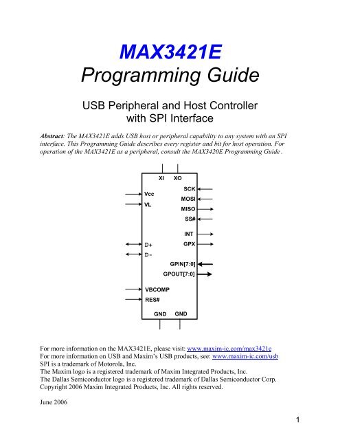
MAX3421E Programming Guide
MAX3421E Programming Guide
MAX3421E Programming Guide

You also want an ePaper? Increase the reach of your titles
YUMPU automatically turns print PDFs into web optimized ePapers that Google loves.
Table 2. All <strong>MAX3421E</strong> Register Bits, for both PERIPHERAL and HOST Modes(Shaded bits do not change during mode (HOST bit) changes.)Reg Perip.Name Host Name b7 b6 b5 b4 b3 b2 b1 b0 accR0 EP0FIFO — b7 b6 b5 b4 b3 b2 b1 b0 —R1 EP1OUTFIFO RCVFIFO b7 b6 b5 b4 b3 b2 b1 b0 RSCR2 EP2INFIFO SNDFIFO b7 b6 b5 b4 b3 b2 b1 b0 RSCR3 EP3INFIFO b7 b6 b5 b4 b3 b2 b1 b0 —R4 SUDFIFO SUDFIFO b7 b6 b5 b4 b3 b2 b1 b0 RSCR5 EP0BC — 0 b6 b5 b4 b3 b2 b1 b0 RSCR6 EP1OUTBC RCVBC 0 b6 b5 b4 b3 b2 b1 b0 RSCR7 EP2INBC SNDBC 0 b6 b5 b4 b3 b2 b1 b0 —R8 EP3INBC — 0 b6 b5 b4 b3 b2 b1 b0 —R9 EPSTALLS — 0 ACKSTAT STLSTAT STLEP3IN STLEP2IN STLEP1OUT STLEP0OUT STLEP0IN —R10 CLRTOGS — EP3DISAB EP2DISAB EP1DISAB CTGEP3IN CTGEP2IN CTGEP1OUT 0 0 —R11 EPIRQ — 0 0 SUDAVIRQ IN3BAVIRQ IN2BAVIRQ OUT1DAVIRQ OUT0DAVIRQ IN0BAVIRQ —R12 EPIEN — 0 0 SUDAVIE IN3BAVIE IN2BAVIE OUT1DAVIE OUT0DAVIE IN0BAVIE —R13 USBIRQ USBIRQ URESDNIRQ VBUSIRQ NOVBUSIRQ SUSPIRQ URESIRQ BUSACTIRQ RWUDNIRQ OSCOKIRQ RCR14 USBIEN USBIEN URESDNIE VBUSIE NOVBUSIE SUSPIE URESIE BUSACTIE RWUDNIE OSCOKIE RSCR15 USBCTL USBCTL HOSCSTEN VBGATE CHIPRES PWRDOWN CONNECT SIGRWU 0 0 RSCR16 CPUCTL CPUCTL PULSEWID1 PULSEWID0 0 0 0 0 0 IE RSCR17 PINCTL PINCTL EP3INAK EP2INAK EP1INAK FDUPSPI INTLEVEL POSINT GPXB GPXA RSCR18 REVISION REVISION b7 b6 b5 b4 b3 b2 b1 b0 RR19 FNADDR — 0 b6 b5 b4 b3 b2 b1 b0 —R20 IOPINS1 IOPINS1 GPIN3 GPIN2 GPIN1 GPIN0 GPOUT3 GPOUT2 GPOUT1 GPOUT0 RSCR21 IOPINS2 IOPINS2 GPIN7 GPIN6 GPIN5 GPIN4 GPOUT7 GPOUT6 GPOUT5 GPOUT4 RSCR22 GPINIRQ GPINIRQ GPINIRQ7 GPINIRQ6 GPINIRQ5 GPINIRQ4 GPINIRQ3 GPINIRQ2 GPINIRQ1 GPINIRQ0 RCR23 GPINIEN GPINIEN GPINIE7 GPINIE6 GPINIE5 GPINIE4 GPINIE3 GPINIE2 GPINIE1 GPINIE0 RSCR24 GPINPOL GPINPOL GPINPOL7 GPINPOL6 GPINPOL5 GPINPOL4 GPINPOL3 GPINPOL2 GPINPOL1 GPINPOL0 RSCR25 HIRQ HXFRDNIRQ FRAMEIRQ CONDETIRQ SUSDNIRQ SNDBAVIRQ RCVDAVIRQ RWUIRQ BUSEVENTIRQ RCR26 HIEN HXFRDNIE FRAMEIE CONDETIE SUSDNIE SNDBAVIE RCVDAVIE RWUIE BUSEVENTIE RSCR27 MODE MODE DPPULLDN DMPULLDN DELAYISO SEPIRQ SOFKAENAB HUBPRE LOWSPEED HOST RSCR28 PERADDR 0 b6 b5 b4 b3 b2 b1 b0 RSCR29 HCTL SNDTOG1 SNDTOG0 RCVTOG1 RCVTOG0 SIGRSM SAMPLEBUS FRMRST BUSRST LSR30 HXFR HS ISO OUTNIN SETUP EP3 EP2 EP1 EP0 LSR31 HRSL JSTATUS KSTATUS SNDTOGRD RCVTOGRD HRSLT3 HRSLT2 HRSLT1 HRSLT0 R4
ResetsThe <strong>MAX3421E</strong> has three reset sources:1. An internal Power-On-Reset (POR) circuit2. A RES# pin3. A register bit called CHIPRESThere is a fourth way in which a reset can occur. When the HOST bit changes state (switching tohost or peripheral operation), the SIE clears certain register bits.The following section explains the effect of each reset source.<strong>MAX3421E</strong> register bits are clocked from two sources:1. The internal 12MHz oscillator2. The SCLK signal that the CPU supplies to the SPI interface.Asserting the RES# or PWRDOWN reset stops the internal 12MH clock. Most register bits areasynchronously cleared. However, the register bits that are clocked from the SPI interface remainactive so the CPU can control the SPI configuration (e.g., the FDUPSPI bit), USB bus pulldownresistors, and the state of the PWRDOWN bit.Power-On ResetThe SIE clears every register bit. Once out of reset, the SIE sets the following bits to indicateavailable buffers:• IN3BAVIRQ (peripheral)• IN2BAVIRQ (peripheral)• IN0BAVIRQ (peripheral)• SNDBAVIRQ (host)Note: POR sets HOST = 0, defaulting to peripheral operation.Asserting the RES# Pin or Setting CHIPRES = 1These resets stop the internal 12MHz oscillator and clear most register bits, but leave the SPIclockedregister bits undisturbed and still accessible by the CPU. The SPI-clocked register bitsare:• HOSCSTEN• VBGATE• CHIPRES• PWRDOWN• CONNECT• SIGRWU• FDUPSPI6 <strong>MAX3421E</strong> <strong>Programming</strong> <strong>Guide</strong>
Accessing the <strong>MAX3421E</strong> RegistersAn SPI master controls the <strong>MAX3421E</strong> by writing and reading 21 internal registers, R0 throughR20. The SPI master begins every register access by asserting the <strong>MAX3421E</strong> SS# (slave select,active low) pin, and clocking in eight bits that comprise the SPI command byte. Figure 1 showsthe command byte format.b7 b6 b5 b4 b3 b2 b1 b0Reg4Reg3Reg2Reg1Reg00DIR1=wr 0=rdACKSTATFigure 1. SPI command byte. As for all SPI transfers, bit 7 is sent first. The ACKSTAT bit isvalid only in peripheral mode; the <strong>MAX3421E</strong> ignores it in host mode.Reg4:Reg0 set the register address, with valid values 0 to 31. The <strong>MAX3421E</strong> ignores Regvalues above 31. The direction bit sets the direction for subsequent bytes in the transfer. TheACKSTAT bit duplicates a USB control bit (R9 bit 6), and is valid only when the <strong>MAX3421E</strong>operates as a USB peripheral. The SIE ignores the ACKSTAT bit when HOST = 1.After sending the command byte, the SPI master transfers one or more bytes in the directionindicated by the DIR bit. Keeping SS# low, the SPI master provides additional bursts of eightSCK pulses for each byte. When the byte transfers are complete, the SPI master de-asserts SS#(drives high) and the transfer terminates.The <strong>MAX3421E</strong> has two register types, FIFOS and control registers. Repeated reads or writes toa register have different effects, depending on the register type.Registers R1, R2, and R4 access internal FIFOS. After selecting the register number with thecommand byte, the SPI master loads or unloads consecutive FIFO bytes by repeating reads orwrites during the same SPI transfer (maintaining SS# low). To write 45 bytes into theSENDFIFO, for example, the SPI master would perform the following steps:1. Set SS# = 0 to start the transfer.2. Issue eight SCLK pulses and send the command byte 00010010. This command byteselects R2 (SNDFIFO) for a write operation (DIR = 1).3. Issue eight SCK pulses, each clocking a data bit into the SNDFIFO register, one bit perSCK rising edge. Every byte the SIE writes the FIFO byte and advances an internal FIFOaddress pointer.4. Repeat Step 3 for 44 more times, clocking in a total of 45 bytes into the SNDFIFO.5. Set SS# = 1 to terminate the transfer.Registers R13 through R31 are <strong>MAX3421E</strong> control registers. If the SPI master repeatedly readsor writes R13 through R20 during the same SPI transfer (SS# low), every byte read or writeautomatically increments the internal register address. This action allows reading or writingconsecutive registers without writing a new command byte to set each new register address. Theregister address continues to increment in this manner until R20 is reached, at which point the8 <strong>MAX3421E</strong> <strong>Programming</strong> <strong>Guide</strong>
egister address “sticks” at R20. This feature gives the microprocessor quick access to the IOpins in R20. For example, to output a prestored waveform on a GPIO pin, the SPI master canwrite the command byte 10100010 (R20, Write) and then send multiple data bytes to R20 tooutput the waveform.If the SPI master explicitly addresses R21 or above, the register addresses again automaticallyincrement during the same SS# transfer until R31 is reached, at which point it “sticks” again atR31.MISO Values for the First Eight Bits in Full-Duplex ModeWhen FDUPSPI = 1, the <strong>MAX3421E</strong> operates its SPI port in full-duplex mode, meaning thatdata is simultaneously clocked in from the MOSI pin and out to the MISO pin on each SCLKrising edge. The first eight bits of an SPI access constitute the command byte, clocked into theMOSI pin. The <strong>MAX3421E</strong> sends status data on the MISO pin while the command byte isclocked into the MOSI pin. The status bits ,while operating in HOST mode, are shown inFigure 2.b7 b6 b5 b4 b3 b2 b1 b0HXFRDNIRQFRAMEIRQCONNIRQSUSDNIRQFigure 2. MISO data when FDUPSPI (HOST = 1).SNDBAVIRQRCVDAVIRQRSMREQIRQBUSEVENTIRQ9
<strong>Programming</strong> Host TransfersWhen HOST = 1, you need to think like a host. Instead of responding to host requests, yougenerate them. This means every packet you send out requires:• A function address in the FNADDR register• An endpoint number in EP[3:0] of the HXFR register• A Packet ID (PID) in the HXFR register• Some data: OUT data in the SNDFIFO (SNDBC bytes, to be exact), or IN data in theRCVFIFO (RCVBC bytes)The function address and endpoint FIFO data persist in the <strong>MAX3421E</strong> until the CPU changesthem. This means, for example, to resend an OUT packet (due to an error by the peripheral) theCPU does not need to load the SNDFIFO again. It just launches the same transfer by rewritingthe HXFR register.The <strong>MAX3421E</strong> does the USB housekeeping work. Set up the above bits, launch the transfer bywriting the HXFR register, wait for a completion interrupt, and check the HRSLT bits (HostResult) to see transfer results. Although the <strong>MAX3421E</strong> reports 16 host result conditions, youwill usually see one of the results shown in Table 3.Table 3. Host Result Codes for Normal USB OperationHSRLT Label Meaning0x00 hrSUCCESS Successful Transfer0x01 hrBUSY SIE is busy, transfer pending0x04 hrNAK Peripheral returned NAK0x05 hrSTALL Perpheral returned STALLAll 16 HRSL codes are shown on page36. None of the conditions in Table 3 represents electricalor signaling errors; they occur in normal USB operations. The hrBUSY result is for applicationsthat do not use the HXFRDN interrupt request to determine when a transfer completes, butinstead poll the HRSL register to check for transfer completion.The host can launch seven transfer types, shown in Table 4.Table 4. HXFR Register Bit Settings for Different Transfer TypesXfr Type HS ISO OUTNIN SETUP hexSETUP 0 0 0 1 0x10BULK-IN 0 0 0 0 0-epBULK-OUT 0 0 1 0 2-epHS-IN 1 0 0 0 0x80HS-OUT 1 0 1 0 0xA0ISO-IN 0 1 0 0 4-epISO-OUT 0 1 1 0 6-epThe CPU can write the HXFR register any time when the SIE is not busy with another transfer.The SIE takes care to avoid collisions with its automatically generated SOF/KA frame markers.10 <strong>MAX3421E</strong> <strong>Programming</strong> <strong>Guide</strong>
If the CPU writes the HXFR register late enough in a frame that the ensuing transfer wouldcollide with the frame marker, the SIE automatically defers sending the packet until after itgenerates the next frame marker.Note: A USB host transfers data over BULK and INTERRUPT endpoints using identicalmethods. The only difference between these two transfer types is when the packets arescheduled, a function of the controlling firmware. This document refers to BULK transfers withthe understanding that any BULK discussion also applies for INTERRUPT transfers.About <strong>MAX3421E</strong> Data TogglesUSB protocol tags every data packet with one of two PIDs (Packet ID’s) called DATA0 andDATA1. These PIDs help detect USB errors. Associated with every endpoint is a data togglevalue, which determines which DATA PIDs to use. The first data packet (after reset) to or froman endpoint is sent using the DATA0 PID. When both sides, the sending and receiving ends,agree that the data is accurate (by generating/receiving the ACK handshake), they bothcomplement their toggle values. Therefore, consecutive data packets sent to or received from anendpoint normally will have toggling PID values—DATA0, DATA1, DATA0, etc.The <strong>MAX3421E</strong> provides four bits to maintain the data toggles. After a data transfer to anendpoint, the SIE updates bits RCVTOGRD and SNDTOGRD (page 36) to indicate the togglevalues for the selected endpoint. The CPU reads and stores these bits to re-initialize the togglevalue for the same endpoint when necessary. To initialize the toggle state before transferring toan endpoint, the CPU sets one of the bit pairs SNDTOG1-SNDTOG0 for OUT data, orRCVTOG1-RCVTOG0 for IN data (page 59). Only one of these bit pairs should be set at a time.The CPU does not need to initialize an endpoint’s toggle value for multiple consecutive transfersto the same endpoint. The <strong>MAX3421E</strong> updates the data toggle value as it performs transfers tothe endpoint. Only when the CPU switches endpoints does it need to restore the data toggle bitsto the values that it saved for the endpoint.11
<strong>Programming</strong> BULK-OUT TransfersThe <strong>MAX3421E</strong> sends BULK data to a peripheral using OUT packets, SNDFIFO data, andhandshakes.The CPU first checks for SNDBAVIRQ = 1 (page 56) to see if the send buffer is available forloading. (The SIE sets this interrupt request bit whenever an OUT transfer successfullycompletes.) If the buffer is available, the CPU writes up to 64 data bytes into the SNDFIFO(page 58) by repeatedly writing R2. Then the CPU writes the byte count (the number of bytes itloaded into the SNDFIFO) into the SNDBC register (page 57). Loading the SNDBC registercauses the SIE to negate the SNDBAVAIRQ bit.Note: If the second buffer of the double-buffered SNDFIFO is free, the SIE immediatelyreasserts the SNDBAVIRQ bit.The CPU may need to initialize the data toggle value for the desired endpoint:• If the transfer is to a new endpoint, the CPU initializes the data toggle to the last savedvalue for the endpoint.• If the endpoint is the same as for the last transfer, the CPU does not need to initialize thedata toggle value. The SIE updates the data toggle after each transfer.Finally, the CPU loads the HXFR register with the value 0010eeee (Table 4) where eeee is theendpoint number to which it is sending the data. The HXFR register is load-sensitive, whichmeans that when the CPU loads the HXFR register, the SIE initiates the transfer.The SIE sends an OUT token, the address in the PERADDR register, the endpoint number inEP[3:0], a CRC5, and EOP. The SIE immediately follows this by sending a DATA0 or DATA1PID (depending on the state of the toggle bit), SNDBC bytes from the SNDFIFO, and a CRC16.Then the SIE waits 6.5 bit times for the peripheral to respond.Note: If SNDBC = 0, the SIE sends no data bytes, but does send the DATA0/1 PID.When the SIE receives a handshake or bus timeout, it sets HXFRDNIRQ = 1 and indicates theresults in the HRSLT[3:0] bits (page 36).If the peripheral returns the ACK handshake, the SIE also complements the data toggle, indicatesa successful transfer (HRSLT[3:0] = 0000), and asserts the SNDBAVIRQ indicating “SendBuffer Available.”If the peripheral did not ACK the transfer, the data may need to be resent. For example, a NAKhandshake is a common response used by a peripheral to indicate that it is not ready to accept thedata. The CPU discovers the cause of a non-ACK’d OUT transfer by examining the HRSLT bits.The CPU relaunches the OUT transfer simply by rewriting HXFR = 0010eeee. The SIE uses thesame values of PERADDR and SNDBC to send the same data in the SNDFIFO.12 <strong>MAX3421E</strong> <strong>Programming</strong> <strong>Guide</strong>
<strong>Programming</strong> BULK-IN TransfersThe CPU issues an IN token to request a peripheral to send it BULK data . Then the SIEtransfers data into its RCVFIFO, and ACKS the transfer.The CPU writes HXFR = 0000eeee (Table 4) to initiate the IN transfer, where eeee is thedesired endpoint address.The SIE sends an IN token, the address in the PERADDR register, the endpoint number inEP[3:0], and a CRC5. It then waits 6.5 bit times for the peripheral to respond. If the peripheralresponds with a DATA0 or DATA1 PID followed by data, the SIE loads the received data bytesinto the RCVFIFO and counts the bytes. At the end of the packet the SIE checks the packet forerrors, updates the RCVBC register and HRSLT bits, and then asserts the HXFRDNIRQ bit.Depending on the transfer outcome, the SIE may or may not assert the RCVDAVIRQ.If the IN data was error-free (HRSLT = 0000), the SIE sends an ACK token, complements thedata toggle, and asserts the RCVDAVIRQ to indicate that new IN data is valid.If the IN data was error-free but there was a data toggle mismatch (the DATA0 or DATA1 PIDsend by the peripheral did not match the endpoint toggle value), the SIE sends the ACKhandshake, but it does not complement the data toggle or assert the RCVDAVIRQ. The SIE setsHRSL = 0110 (Toggle Error) for this condition. This situation would happen if the peripheralreceived a corrupted ACK handshake from the previous IN transfer. In this case the host ignoresthe data in the RCVDATA FIFO, because it represents data that the peripheral mistakenly resentwhen it missed the last ACK handshake. By ACK-ing the transfer and not updating its owntoggle bit, the SIE causes the peripheral to complement its toggle bit, thus forcing the data togglemechanism back into sync.If the HRSLT bits indicate a data error, the SIE does not send the ACK, complement the datatoggle, or assert the RCVDAVIRQ bit.The CPU responds to the HXFRDNIRQ indication by examining the result bits in HRSLT[3:0].If the result is 0000 (success), the CPU reads RCVBC to determine the byte count, and thenreads that number of bytes using repeated reads to the RCVFIFO register (page 48). After theCPU retrieves the data, it clears the RCVDAVIRQ bit (by writing 1 to it). If there is anotherbuffer of IN data in the double-buffered RCVFIFO, the SIE immediately re-asserts theRCVDAVIRQ bit.Note: The SIE does not automatically retry an IN transfer that indicates an error. Instead, itnotifies the CPU (through the HXFRDNIRQ and HRSLT bits) of the error and generates thecorrect USB response. Usually the CPU will simply resend the IN packet by reloading the HXFRregister.13
<strong>Programming</strong> a CONTROL TransferA host sends a CONTROL transfer in two or three stages:1. A SETUP packet, which sends 8 bytes of “op-code” to the peripheral2. An optional data stage, usually a BULK IN request3. A status stageThe host sends CONTROL transfers to a peripheral’s default control endpoint zero.1. SetupThe CPU writes the 8-byte SETUP data into the SUDFIFO. There is no byte count registerassociated with the SUDFIFO because the SETUP packet payload is always 8 bytes. Then theCPU loads the HXFR register with the value 00010000 (Table 4), which instructs the SIE todispatch a SETUP packet to endpoint zero.The SIE then sends a SETUP packet consisting of a SETUP PID, the address in the PERADDRregister, endpoint 0000, a CRC5, and EOP, and follows with a DATA0 packet containing the 8bytes in the SUDFIFO. The SIE waits 18 bit times for the device to respond or time out, andfinally terminates the transfer by asserting the HXFRDNIRQ bit and updating the HSRLT bits(page 36). The USB spec says that a peripheral must always ACK a SETUP packet.Note: The SIE sends fixed DATA0 and DATA1 PID tokens for the various stages of aCONTROL transfer, regardless of the setting of the internal data toggle.2. Data (optional)If a data stage is required, it is programmed as a BULK-IN or BULK-OUT transfer. SomeCONTROL transfers, such as Set_Address, do not require a data stage because the commanddata fits into the 8 bytes in the SETUP packet.3. StatusUnique to CONTROL transfers, the status stage provides an added measure of protection forthese mission-critical transfers. A status stage consists of an IN or OUT packet in the oppositedirection as the preceding stage.A STATUS packet is a BULK-OUT or BULK-IN transfer that contains no data and whichalways uses the DATA1 PID. The programmer could send these transfers by programmingstandard BULK transfers. For convenience, however, the <strong>MAX3421E</strong> provides special HS-OUTand HS-IN launch codes for handshakes so the SIE can do the work.HS-OUTThe host sends the OUT handshake to terminate a CONTROL-READ request such asGet_Descriptor. To send an OUT handshake packet, the CPU loads the HXFR register with thevalue 0xA0 (Table 4).The SIE sends the OUT PID, the address in PERADDR, endpoint zero, and a CRC5 value. TheSIE then sends a DATA1 PID, and waits 6.5 bit times for the peripheral to respond or time out.14 <strong>MAX3421E</strong> <strong>Programming</strong> <strong>Guide</strong>
Note that this is identical to a BULK-OUT packet with no data and a fixed DATA1 PID. Whenthe SIE receives a handshake or bus timeout, it sets HXFRDNIRQ = 1 and indicates the resultsin the HRSLT[3:0] bits (page 36).HS-INThe host sends the IN handshake to terminate a CONTROL-WRITE request such asSet_Address. To send an IN handshake packet, the CPU loads the HXFR register with the value0x80 (Table 4).The SIE sends the IN PID, the address in PERADDR, endpoint zero, and a CRC5 value, thenwaits 6.5 bit times for the peripheral to respond. Then the SIE updates the HRSLT bits andasserts the HXFRDNIRQ bit. If the peripheral returns the DATA1 PID (with no data), the SIEautomatically sends an ACK handshake indicating successful termination of the CONTROLtransfer.About ISO TransfersUSB ISOCHRONOUS transfers are characterized by on-time delivery without the handshakesthat accompany the other USB transfer types. Once a USB host enumerates a device and grantsits ISO bandwidth requirements (bandwidth indicates the number of bytes allocated to the ISOendpoint in every 1-millisecond frame), the USB spec requires the host to deliver or consumethat number of bytes every frame.This gives rise to special consideration for the <strong>MAX3421E</strong>, which may be connected to a slowSPI interface or CPU. The controller must keep pace with the scheduling requirements. If there isa speed mismatch, the <strong>MAX3421E</strong> has two ways to indicate the problem, as set by theDELAYISO bit.Double BufferingThe <strong>MAX3421E</strong> SNDFIFO and RCVFIFO are double-buffered, meaning that each has two setsof 64-byte FIFOS and byte count registers. This double-buffering is essential for performing ISOtransfers larger than one maximum packet size of 64 bytes. The double-buffer feature is invisibleto the programmer:• INs: If the CPU clears the RCVDAVIRQ (Receive Data Available IRQ) bit afterunloading the RCVFIFO, and if there is another packet of data waiting in the otherbuffer, the SIE immediately re-asserts the RCVDAVIRQ bit.• OUTs: If the CPU clears the SNDBAVIRQ (Send Buffer Available IRQ) by loading theSNDBC register with the number of bytes which it loaded into the SNDFIFO, and if theother buffer is available for loading, the SIE immediately re-asserts the SNDBAVIRQbit.Although the SNDFIFO and RCVFIFO are 64 bytes, the SIE can send and receive ISO datapackets of any size (up to the USB spec limit of 1023 bytes) by concatenating data fromconsecutive loads/reads of these FIFOS into one large data packet, as long as the CPU suppliesor consumes the data in time.15
The SIE detects the end of an ISO IN data packet by detecting the EOP (End-Of-Packet) buscondition. For OUT transfers, the SIE normally detects the end of a data payload when the CPUloads a FIFO with fewer than 64 bytes. This works either for a single packet (63 or fewer bytes),or a data payload that spans multiple 64-byte buffer loads where the last buffer contains 63 orfewer bytes. However, there is a special case when the last packet of data is exactly 64 bytes.The SIE needs to know whether this represents another 64 bytes in a multibuffer load, or if it isthe last 64 bytes in a transfer whose length is an exact multiple of 64 bytes. The CPU informs theSIE that a 64 byte packet represents the end of the OUT transfer by loading SNDBC = 0. This isa special signal to the SIE, which does not take its normal action of switching buffers when theSNDBC register is loaded.<strong>Programming</strong> ISO-IN TransfersThe CPU writes HXFR = 0100eeee to initiate an ISO IN transfer.The SIE sends an OUT token using the address in the PERADDR register, the endpoint numberin EP[3:0], a CRC5, and EOP. It then waits 6.5 bit times for a DATA0 PID or bus timeout. If theSIE receives the DATA0 PID, it begins loading data into the RCVFIFO. When the FIFO fillswith 64 bytes (or the end-of-packet signal is indicated on the bus), the SIE writes the byte countto RCVBC and asserts the SNDBAVIRQ, thereby indicating that a FIFO is available for theCPU to load more data if necessary. At the end of the ISO IN transfer (EOP), the SIE updates theHRSLT bits and asserts the HXFRDNIRQ.<strong>Programming</strong> ISO-OUT TransfersThe SIE master sends an OUT packet to the peripheral, followed by a data packet using the fixedDATA0 PID. There are three cases to consider:1. OUT data payload sizes of fewer than 64 bytes2. Exactly 64 bytes3. More than 64 bytes.1. OUT Payload Fewer than 64 BytesThe CPU programs this similarly to a BULK transfer. The CPU loads bytes into the SNDFIFO,and writes the byte count into SNDBC. Then it writes the HXFR register with 0110eeee (Table4) to launch the transfer.The SIE sends an OUT token using the address in the PERADDR register, the endpoint numberin EP[3:0], a CRC5, and EOP. The SIE immediately follows by sending a DATA0 PID, SNDBCbytes from the SNDFIFO, and a CRC16. Then, recognizing SNDBC
OUT Payload Greater than 64 BytesThe CPU loads the SNDFIFO with 64 bytes of data, then writes SNDBC = 64. If SNDBAVIRQ= 1, it can load the second portion of the data packet into the SNDFIFO, after which it againwrites the SNDBC register with the byte count. To launch the transfer it loads HXFR registerwith 0110eeee.As a FIFO becomes available, the SIE continues to assert SNDBAVIRQ, asking for the nextchunk of ISO OUT data. The double-buffering allows the SIE to send OUT data from one FIFOwhile the CPU loads the other one.The SIE terminates the ISO OUT transfer by updating the HRSLT bits and asserting theHXFRDNIRQ. An ISO OUT transfer terminates after the SIE transmits the last byte of a FIFOwith an associated SNDBC
Active Bits in Peripheral and Host ModesSome <strong>MAX3421E</strong> features are available for both peripheral and host operation. These featuresinvolve non-USB system aspects such as how the SPI master is configured, how the interrupt pinoperates, and the state of the IO pins. These features can be grouped as follows:• Interface Configurationo FDUPSPIo GPX[B:A]o INTLEVELo POSINT• IO Pin configuration and Output Valueso GPIN pins—interrupt polarity and enableso GPOUT pin stateso VBCOMP pin detected level• Global Chip Operationso CHIPRESo PWRDOWNo OSCOK (Oscillator OK)• Some IRQ Bits and the IE BitTable 2 shows the registers and bits that persist when the SPI master commands a <strong>MAX3421E</strong>mode change, either from peripheral to host or from host to peripheral. Therefore, a mode changedoes not disturb the SPI interface configuration or the GPOUT pin values. The IE bit and theGPIN interrupt bits (GPINIRQ and GPINIE) remain unchanged through a mode change. Thismeans that if a GPIN interrupt is pending before the mode change, it will be pending after themode change.Note: There are two ways to command the <strong>MAX3421E</strong> to switch from HOST to PERIPHERALoperation. First, the SPI master can write a zero to the HOST bit in the MODE register R27.Second, the SPI master can set, then clear the CHIPRES bit in the USBCTL register R16. UsingCHIPRES is the preferred way if you want to start with a “clean” peripheral.18 <strong>MAX3421E</strong> <strong>Programming</strong> <strong>Guide</strong>
BUSEVENTIRQ, BUSEVENTIEMeaning: BUSEVENTIRQ: One of two bus events has occurred.BUSEVENTIE: Enable the BUSEVENTIRQ.Mode:Host onlyThe SIE sets the BUSEVENTIRQ bit when it completes signaling one of two USB bus events:• Bus Reset (when BUSRST 1→0)• Bus Resume (when BUSRSM 1→0)The CPU clears the BUSEVENTIRQ bit by writing a 1 to it.The CPU sets and clears the BUSEVENTIE bit. When BUSEVENTIE = 1, the BUSEVENTIRQis enabled as a source to activate the INT pin.<strong>Programming</strong> NotesThis interrupt is shared by two sources: completion of bus reset signaling, or bus resumesignaling. As this is a shared interrupt, it is good practice to clear the BUSEVENTIRQ bit beforeinitiating either of the two bus signals (before setting BUSRST = 1 or BUSREM = 1).19
BUSRSTMeaning:Mode:Issue a Bus Reset to a USB peripheral.Host onlyThe CPU sets this bit to initiate a 50ms bus reset (SE0) signal to the peripheral.The SIE clears this bit at the conclusion of the bus reset signaling.The CPU may also clear this bit to prematurely terminate the 50ms SE0 bus signal. Terminatingthe reset signal in this manner causes the BUSEVENTIRQ to assert.<strong>Programming</strong> NotesThe CPU sets this bit to instruct the SIE to issue a bus reset on the D+ and D- lines. After settingthis bit, the CPU can detect the end of the 50ms interval either by polling the BUSRST bit forzero, or by responding to the BUSEVENTIRQ. To program a bus reset, follow this sequence ofsteps:1. Set BUSRST = 1.2. Test for BUSRST = 0 or respond to the BUSEVENTIRQ.3. Turn on frame markers by setting SOFKAENAB = 1.4. Wait for at least one FRAMEIRQ.Step 4 ensures that the host logic is ready to generate the first host transaction.20 <strong>MAX3421E</strong> <strong>Programming</strong> <strong>Guide</strong>
CHIPRESMeaning:Mode:Chip ResetPeripheral and HostThe CPU sets this bit to reset the chip. Its effect is identical to driving the RES# pin low.The CPU clears this bit to take the chip out of reset.<strong>Programming</strong> NotesThe CPU can clear this bit immediately after setting it. Resetting the <strong>MAX3421E</strong> either at poweron or by setting the CHIPRES bit clears most register bits, including the HOST bit, and thereforesets up the <strong>MAX3421E</strong> to operate as a USB peripheral device.Setting CHIPRES = 1 stops the internal oscillator. After removing the reset by settingCHIPRES = 0, the CPU should check the OSCOK interrupt request. The CPU should proceedonly after this interrupt asserts, an indication that the oscillator and PLL have stabilized.21
CONDETIRQ, CONDETIEMeaning: CONDETIRQ: Peripheral Connect/Disconnect Interrupt RequestCONDETIE: Peripheral Connect/Disconnect Interrupt EnableMode:Host onlyThe SIE sets the CONDETIRQ bit to indicate that a peripheral has either plugged in orunplugged. The CPU clears the CONDETIRQ bit by writing a 1 to it. The conditions thatactivate the CONDETIRQ bit are:• The bus makes a transition from the J-state or K-state to 25 microseconds of SE0. Thisindicates that a peripheral device has disconnected.• The bus makes a transition from 8 SE0 bit times to 25 microseconds of the J-state or K-state. This indicates that a peripheral device has connected.The CPU sets and clears the CONDETIE bit. When CONDETIE = 1 the CONDETIRQ isenabled as a source to activate the INT pin.<strong>Programming</strong> NotesTo detect a peripheral connect or disconnect, the CPU should first set HOST = 1 to put the<strong>MAX3421E</strong> into host mode. It should then set DPPULLDN = 1 and DMPULLDN = 1 toestablish logic low levels for the D+ and D- signals.To determine whether connect or disconnect occurred, the CPU reads the HSRL register andexamines the JSTATUS and KSTATUS bits. Normally these status bits update when the CPUsets the SAMPLEBUS bit, but they also automatically update when the CONDETIRQ interruptasserts.22 <strong>MAX3421E</strong> <strong>Programming</strong> <strong>Guide</strong>
ISO OUTS with DELAYISO = 0If an ISO-OUT data packet transfer is underway when it is time for the SIE to generate the nextSOF packet, the SIE truncates the data packet and generates the SOF. The SIE indicates this lossof-datacondition by setting HRSLT[3:0] = 0x03, followed by the FRAMEIRQ. It does not assertthe HXFRDNIRQ in this case.ISO OUTS with DELAYISO = 1The SIE delays sending the OUT data packet if the CPU writes the HXFR register at a time thatwould not allow the SIE to transfer 256 bytes before the end of the frame. In this case the SIEsends the next SOF packet (and asserts FRAMEIRQ); it then sends the delayed ISO packet andterminates the transfer, asserting the HXFRDNIRQ with code 0x00 (hrSUCCESS). The CPUdetects a deferred packet by sampling the SNDBAVIRQ bit just after the FRAMEIRQ. IfSNDBAVIRQ is zero, the SNDFIFO buffer is still committed to USB transfer and the packetwas therefore delayed.ISO IN-SOF ConflictsThe SIE handles IN transfer conflicts somewhat differently than for OUTS, because the hostcannot command a peripheral to stop sending data to avoid colliding with the next SOF packet.Therefore, in the conflict condition the SIE either reads the remaining ISO IN data and does notgenerate the SOF packet, or it delays sending the IN request until after it generates the next SOFpacket.Note: Another ISO error condition is a data over-run, indicated by the result codeHRSLT = 0x06. A data over-run occurs when the SIE has ISO IN data available but nowhere toput it. This happens because no RCVFIFOS are available (the CPU has not unloaded theRCVFIFO in time.ISO INS with DELAYISO = 0If an ISO-IN request results in the peripheral sending a data packet that runs past the SOFgeneration time, the SIE continues to receive the IN data and suppresses sending the SOF packetfor that frame. In this case the SIE sets HRSLT[3:0] = 0x03, does not assert the HXFRDNIRQwhen the IN transfer completes, but does assert the FRAMEIRQ for that frame. The CPU candetect this error case by recognizing that a FRAMEIRQ occurred without an HXFRDNIRQbefore it.Note: The SIE always increments the frame count, whether or not an SOF packet is actually sent.ISO INS with DELAYISO = 1If the CPU initiates the ISO-IN transfer at a time that would not allow a 256 byte data packet tobe received before colliding with the next SOF, the SIE defers sending the IN packet until afterthe next frame. In this case the SIE asserts the FRAMEIRQ for the next frame, sends the ISO-INpacket, transfers the IN data, and asserts the HXFRDNIRQ with HRSLT[3:0] = 0x00(hrSUCCESS).24 <strong>MAX3421E</strong> <strong>Programming</strong> <strong>Guide</strong>
Note: If ISO scheduling problems are detected, the system must be modified to dispatch the ISOpackets earlier in each frame, perhaps by speeding up the SPI interface, tuning the firmware, orboth.25
FDUPSPIMeaning:Mode:Full-Duplex SPI port operationPeripheral and HostThe CPU sets this bit to operate the SPI port in full-duplex mode.The CPU clears this bit to operate in half-duplex mode.POR: FDUPSPI = 0 (half-duplex)Chip Reset: No changeBus Reset: No changePwr Down: Read-write<strong>Programming</strong> NotesHalf-duplex SPIIn half-duplex mode (FDUPSPI = 0), the MOSI (Master Out, Slave In) pinbecomes a bidirectional IO pin, and the MISO (Master In, Slave Out) pin is tri-stated.FDUPSPI=0 (default)8-bit SRMOSISPI DirectionMISOFigure 3. Half-duplex SPI interface.Full-Duplex SPIFull-duplex mode (FDUPSPI = 1) provides separate MOSI and MISO pins. This configurationhas the added feature that while the first byte of every transfer (the command byte) is clocked in,eight bits of status information are simultaneously clocked out.FDUPSPI=1MOSI8-bit SRMISOFigure 4. Full-duplex SPI interface.27
The SPI Command ByteThe first byte clocked into the SPI interface is a command byte that sets: the register address; thedirection; and when operating as a USB peripheral device, a bit that directly sets the ACKSTATbit. In all SPI transactions, whether in or out, the bit ordering is b7 first, b0 last.MOSI Bit Signal7 REG46 REG35 REG24 REG13 REG02 01 Direction (1= Wr, 0 = Rd)0 ACKSTAT (peripheral)Figure 5. The SPI command byte.An SPI cycle starts with the SPI master driving CS# low, then driving eight SPI clocks whoserising edges strobe in the command byte. REG[4:0] set the register address, and the direction bitsets the read or write direction for the SPI cycle. For USB peripheral operation, the ACKSTATbit writes the corresponding bit in the EPSTALLS register.Following the command byte, the SPI master issues one or more groups of 8-SCK clocks toclock byte data into or out of the <strong>MAX3421E</strong>. When accessing a FIFO, as long as CS# remainslow, the register address clocked in with the command remains in effect. This ability to burstbytes is convenient when reading or writing the endpoint FIFOS. For example, to load 37 bytesinto the EP0FIFO (peripheral mode), the SPI master writes the command byte 00000010 whichselects R0 (EP0FIFO) for a write operation (direction bit is 1). Then it writes 37 bytes to the SPIport, and finally drives CS# high to complete the SPI cycle.Note: Both MOSI and MISO data are sampled on the rising edge of SCK. Data changes on thefalling edge of SCK.The SPI cycle terminates when the SPI master return CS# to its high state.SPI ModesThe SPI standard defines four clocking modes, reflecting two mode signals called CPOL (clockpolarity) and CPHA (clock phase). These signals are represented in the form (CPOL, CPHA). Aninterface that expects both positive edge SCKS and the MOSI data to be available before the firstpositive clock edge, can operate in modes (0,0) and (1,1) without alteration. This property allowsthe <strong>MAX3421E</strong> to operate in mode (0,0) or (1,1) without requiring a mode pin.The scope traces below illustrate identical data transfers between a microprocessor and the<strong>MAX3421E</strong>. Figure 6 uses SPI mode (0,0) and Figure 7 uses SPI mode (1,1). The difference is28 <strong>MAX3421E</strong> <strong>Programming</strong> <strong>Guide</strong>
the inactive level of the SCK signal, low for mode (0,0) and high for mode (1,1). In both modesthe MOSI and MISO data sampled by the rising edge of SCK is the same.Figure 6. SPI interface operating in mode (0,0).Figure 7. SPI interface operating in mode (1,1,).29
FRAMEIRQ, FRAMEIEMeaning: FRAMEIRQ: Frame Generator Interrupt RequestFRAMEIE: Frame Generator Interrupt EnableMode:Host onlyThe SIE sets the FRAMEIRQ bit whenever it generates a 1-millisecond frame marker, thatconsists of a full-speed SOF packet or a low-speed keep-alive pulse. The CPU clears theFRAMEIRQ bit by writing a 1 to it.The CPU sets and clears the FRAMEIE bit. When FRAMEIE = 1, the FRAMEIRQ is enabled asa source to activate the INT pin.<strong>Programming</strong> NotesAt full speed, the SIE sets the FRAMEIRQ interrupt at the beginning of the SOF packet.30 <strong>MAX3421E</strong> <strong>Programming</strong> <strong>Guide</strong>
FRMRSTMeaning:Mode:Reset the SOF frame counterHost onlyThe CPU sets this bit to clear the frame counter.The SIE clears this bit to indicate that it has completed the operation.<strong>Programming</strong> NotesThis bit has meaning only when the <strong>MAX3421E</strong> is operating as a full-speed host. (Whenoperating as a low-speed host, there is no SOF packet or frame count.) After settingFRMRST = 1, the next SOF packet will contain a frame count of zero.The <strong>MAX3421E</strong> clocks its frame counter using an internal prescaler. Setting FRMRST = 1 resetsthe frame count but not the prescaler, thus ensuring a steady stream of SOF packets everymillisecond.31
GPIN(0-7), GPINPOL(0-7)GPINIRQ(0-7), GPINIE (0-7)Meaning: GPIN General-Purpose Input pins 0 through 7GPINPOL General-Purpose IN Interrupt Polarity 0 though 7GPINIRQ General-Purpose IN Interrupt Request 0 through 7GPINIE General-Purpose IN Interrupt Enable 0 through 7Mode:Peripheral and HostGPINThe CPU reads the GPIN pin states by reading the GPIN register bits. Only the outside circuitrycan control these register bit states. All eight GPIN pins are pulled up to V CC with weak (~20kΩ) internal resistors.GPINPOLThe CPU sets the GPINPOL bits to set the edge polarity of the interrupt requests for each of theGPIN pins (Table 5). These bits are cleared at power-on. They retain their states either whenCHIPRES = 1 or after a mode change.Table 5. Edge Polarity for the GPIN InterruptsGPINPOL Polarity0 neg edge1 pos edgeGPINIRQThe <strong>MAX3421E</strong> sets a GPIN Interrupt Request bit when a signal on the GPIN pin makes apositive or negative transition. The GPINPOL bit (Table 5) controls the active edge polarity.The GPINIRQ bits are active whether or not the individual GPIN interrupt enables or the IE bitis set.GPINIEThe CPU sets a GPIN Interrupt Enable bit to pass the corresponding IRQ bit through to theinterrupt logic feeding the <strong>MAX3421E</strong> INT pin. If IE = 1, an enabled IRQ appears either on theINT pin if SEPIRQ = 0, or on the GPX pin if SEPIRQ = 1 and GPX[B:A] = 10.Note: During normal operation, the GPIN interrupts are OR’d with all the other <strong>MAX3421E</strong>interrupt sources indicated on the INT pin. It is also possible to detach the eight GPIN interruptrequest bits as INT pin sources and make them separately available as a group on the GPX pin.In this mode, the GPX pin serves as a second <strong>MAX3421E</strong> INT output pin. This mode may bepreferred in systems that need to minimize detection time for external events. The SEPIRQ bitenables this separation of interrupt sources.32 <strong>MAX3421E</strong> <strong>Programming</strong> <strong>Guide</strong>
GPOUT(0 through 7)Meaning: General-Purpose Output pins 0 through 7Mode:Peripheral and HostThe CPU sets and clears these bits.<strong>Programming</strong> NotesThe CPU writes these bits to control the states of the GPOUT pins. The output voltages arereferenced to the voltage on the VL pin. The CPU can also read these bits. Reading the bitindicates the state of the output flip-flop that drives the output buffer. Therefore, if the output pinis driving a large load (e.g., an LED) which compromises the logic level, the CPU will read thecorrect logic state of the output pin.33
GPXB, GPXAMeaning:Mode:Two bits, GPXB and GPXA, determine the output of the GPX pin.Peripheral and HostThe CPU sets and clears these bits.<strong>Programming</strong> NotesThe GPX pin can output one of four internal signals, as shown in the table below:GPXB GPXA GPX Pin0 0 OPERATE (complement of internal POR)0 1 VBUS Detect1 0 BUSACT or INIRQ*1 1 SOF (0-1 transition when SOF packetarrives, 50% duty-cycle signal)* If SEPIRQ = 1The default setting for the GPX output when GPXB = 1 and GPXA = 0 is BUSACT. However, ifthe SEPIRQ bit is set to 1, the BUSACT signal is replaced by an interrupt request signal that isactive whenever one of the eight GPIN pins makes a 0-1 or 1-0 transition. In this case the GPXpin serves as a second interrupt pin (along with INT), with the same configuration (level or edge,edge polarity) as the INT pin. See page 53 for more information about the SEPIRQ bit.34 <strong>MAX3421E</strong> <strong>Programming</strong> <strong>Guide</strong>
HOSTMeaning:Mode:<strong>MAX3421E</strong> host or peripheral operationPeripheral and HostThe CPU sets HOST = 1 to operate the <strong>MAX3421E</strong> as a USB host.The CPU sets HOST = 0 to operate the <strong>MAX3421E</strong> as a USB peripheral (default).<strong>Programming</strong> NotesAt power-on or after a RES# pin reset, the <strong>MAX3421E</strong> defaults to peripheral operation with theHOST bit set to 0. In this mode the <strong>MAX3421E</strong> operates as a MAX3420E peripheral-onlycontroller.The CPU sets HOST = 1 to operate the <strong>MAX3421E</strong> as a host. It uses the register set shown inTable 1.<strong>Programming</strong> information for operating when HOST = 0 is found in the MAX3420E<strong>Programming</strong> <strong>Guide</strong>. For reference, Table 2 shows all <strong>MAX3421E</strong> register bits, for bothperipheral and host operation.35
HRSL RegisterHRSLT[3:0]SNDTOGRD, RCVTOGRDMeaning:Mode:These bits indicate the results of a host transfer:• HRSLT[3:0] indicate the result code.• SNDTOGRD and RCVTOGRD indicate the resulting data toggle values forOUT and IN transfers, respectively.Host onlyThe SIE sets and clears these bits.<strong>Programming</strong> NotesThe SIE updates these bits at completion of a host transfer. The CPU reads the HRSL registerafter receiving the HXFRDNIRQ or after polling the HRSL register and reading an HRSLTvalue other than hrBUSY. The HRSLT bits indicate the result of the host transfer, as shown inTable 6.Table 6. HRSLT[3:0] CodesHSRLT Label Meaning0x00 hrSUCCESS Successful Transfer0x01 hrBUSY SIE is busy, transfer pending0x02 hrBADREQ Bad value in HXFR reg0x03 hrUNDEF (reserved)0x04 hrNAK Peripheral returned NAK0x05 hrSTALL Perpheral returned STALL0x06 hrTOGERR Toggle error/ISO over-underrun0x07 hrWRONGPID Received the wrong PID0x08 hrBADBC Bad byte count0x09 hrPIDERR Receive PID is corrupted0x0A hrPKTERR Packet error (stuff, EOP)0x0B hrCRCERR CRC error0x0C hrKERR K-state instead of response0x0D hrJERR J-state instead of response0x0E hrTIMEOUT Device did not respond in time0x0F hrBABBLE Device talked too longThe SNDTOGRD (for an OUT transfer) and RCVTOGRD (for an IN transfer) indicate the datatoggle values resulting from the transfer. The CPU should read and store these values wheneverit finishes a consecutive sequence of transfers to the same endpoint. Doing this allows the CPUto restore the toggle value the next time the CPU transfers data to the same endpoint. The CPUinitializes the endpoint toggle value using the SNDTOG0/1 and RCVTOG0/1 bits in the HCTLregister (page 59).36 <strong>MAX3421E</strong> <strong>Programming</strong> <strong>Guide</strong>
HUBPREMeaning:Mode:Send the PRE PID to a LS device operating through a USB hub.Host onlyThe CPU sets and clears this bit.<strong>Programming</strong> NotesIf the host firmware detects (during enumeration) that it is talking to a low-speed peripheralthrough a USB hub, it sets HUBPRE = 1. This instructs the SIE to precede every low-speedpacket with a full-speed PRE PID, and to do the necessary signaling required by the USBspecification.37
HXFR RegisterEP[3:0]HS, ISO, OUTNIN, SETUPMeaning:Mode:The CPU writes this register to launch a host transfer.Host onlyThe CPU sets and clears these bits.<strong>Programming</strong> NotesThis register is load-sensitive. This means that when the CPU writes it, the SIE launches atransfer. The CPU loads values shown in Table 7 to launch the various USB transfer types.Table 7. HXFR Register Bit Settings for Different Transfer TypesXfr Type HS ISO OUTNIN SETUP hexSETUP 0 0 0 1 10BULK-IN 0 0 0 0 0-epBULK-OUT 0 0 1 0 2-epHS-IN 1 0 0 0 8-epHS-OUT 1 0 1 0 A-epISO-IN 0 1 0 0 4-epISO-OUT 0 1 1 0 6-epThe BULK-IN and BULK-OUT entries apply for transfers either to a BULK or INTERRUPTendpoint. These two transfer types are identical, differing only by when the host firmwareschedules them.The ‘-ep’ field in the ‘hex’ column indicates the value of EP[3:0].For details about each of these transfer types, see “<strong>Programming</strong> Host Transfers” on page 10.38 <strong>MAX3421E</strong> <strong>Programming</strong> <strong>Guide</strong>
HXFRDNIRQ, HXFRDNIEMeaning: HXFRDNIRQ: Host Transfer Done Interrupt RequestHXFRDNIE: Host Transfer Done Interrupt EnableMode:Host onlyThe SIE sets the HXFRDNIRQ bit when it has completed a host transfer. The CPU clears theHXFRDNIRQ by writing a 1 to it.The CPU sets and clears the HXFRDNIE bit. When HXFRDNIE = 1, the HXFRDNIRQ isenabled as a source to activate the INT pin.<strong>Programming</strong> NotesWhen this interrupt asserts, the CPU determines the result of the host transfer by reading theHSRLT bits in the HRSL register (page 36).39
IEMeaning:Mode:Enable the INT pin.Peripheral and HostThe CPU sets this bit to activate the INT output pin. The characteristics of the INT output pin aredetermined by the INTLEVEL, POSINT and PULSEWID[1:0] bits (page 41).The CPU clears this bit to disable the INT output pin.<strong>Programming</strong> NotesWhen IE = 0, the state of the INT pin is inactive (open for level mode, high for negative edge,low for positive edge).The internal IRQ bits operate independent of the state of the IE bit. The IE bit only controlsactivation of the INT output pin.40 <strong>MAX3421E</strong> <strong>Programming</strong> <strong>Guide</strong>
INTLEVELPOSINTPULSEWID1, PULSEWID0Meaning: INTLEVEL: Sets the INT output pin to level-active (1) or edge-active (0).POSINT: Edge polarity of the edge-active INT pin.PULSEWID: These two bits set the IRQ inactive time in edge mode (see below).Mode:Peripheral and HostINTLEVELThe CPU sets the INTLEVEL bit to make the INT output pin level-active. When INTLEVEL= 1the INT pin drives low if one or more enabled interrupts are pending. In this mode the INT pin isopen-drain, so the system must include a pullup resistor to VL.The CPU clears the INTLEVEL bit to make the INT pin edge active. When INTLEVEL= 0, theedge polarity is set by the POSINT bit. In edge output mode the INT pin driver is push-pull, sono pullup resistor to VL is required.POSINTThis bit has effect only when the CPU has programmed the INT pin to be edge-active(INTLEVEL= 0). When POSINT= 1 the INT pin signals pending interrupts with a positive edge,and when POSINT= 0, the INT pin signals pending interrupts with a negative edge.PULSEWID1[0]These bits have effect only when the CPU has programmed the INT pin to be edge-active(INTLEVEL = 0). They control the inactive INT pin time intervals between the CPU clearingone IRQ bit and the INT pin re-asserting due to one or more pending interrupts (Figure 8).41
<strong>Programming</strong> NotesSingleIRQClearIRQFirst IRQActiveSecond IRQActiveClear first IRQ,second IRQstill activeClear lastpending IRQINTLEVEL=1POSINT=XINTLEVEL=0POSINT=XINTLEVEL=0POSINT=X(1)(2)(1) Width determined by clearing the IRQ. Width determined by PULSEWID[1:0].Figure 8. INT pin behavior depending on INTLEVEL and POSINT bits.The waveforms in Figure 8 show the INT pin behavior for different settings of the INTLEVELand POSINT bits.In level mode (top diagram) the INT pin stays low until no interrupt requests are pending. TheINTLEVEL mode is open-drain and requires a pullup resistor from the INT pin to VL.In edge mode the INT pin delivers an edge whenever a new interrupt request occurs or aninterrupt request bit is cleared while others are pending. If an interrupt is pending when anotheris cleared in edge mode, the INT pin momentarily goes inactive, then active again to deliver theedge. The inactive time, shown as (2) in the Figure 8, is programmable to four values, shown inthe table below.PULSEWID1PULSEWID0INT PulseWidth uS0 0 10.60 1 5.31 0 2.61 1 1.3Note: The MAX3420E does not have the PULSEWID[1:0] bits. The MAX3420E time is fixed at10.6μS.When SEPIRQ = 1, the <strong>MAX3421E</strong> removes the eight interrupts associated with the eight GPINpins from the INT pin. The <strong>MAX3421E</strong> then routes them to the GPX pin, which serves as asecond interrupt output pin when GPX[B:A] = 10. When the GPX pin operates in this manner itscharacteristics as an INT output pin are set by the INTLEVEL, POSINT, and PULSEWID[1:0]bits.42 <strong>MAX3421E</strong> <strong>Programming</strong> <strong>Guide</strong>
LOWSPEEDMeaning:Mode:Sets the host for low-speed operationHost onlyThe CPU sets and clears this bit.<strong>Programming</strong> NotesThe CPU sets this bit to enable operation as a low-speed USB host. The CPU will normally setthis bit when it discovers that a peripheral has plugged in (activating CONDETIRQ) and that thequiescent bus state is D+ = 0, D- = 1.This bus condition is indicated by:• LOWSPEED = 1 and a J-state is detected.• LOWSPEED = 0 and a K-state is detected.See page 50 for information about detecting the bus state.43
OSCOKIRQ, OSCOKIEMeaning:Mode:OSCOKIRQ: Oscillator OK Interrupt RequestOSCOKIE: Oscillator OK Interrupt EnablePeripheral and HostAn internal OSCOK signal indicates that the internal 12MHz oscillator and 48MHz PLL arestable and that the chip is ready to operate. The SIE sets the OSCOKIRQ bit when the OSCOKsignal makes a 0-1 transition, indicating that the chip is ready to operate. The CPU clears theOSCOKIRQ bit by writing a 1 to it.The CPU sets and clears the OSCOKIE bit. When OSCOKIE = 1 the OSCOKIRQ is enabled asa source to activate the INT pin.<strong>Programming</strong> NotesWhenever the CPU stops the <strong>MAX3421E</strong> oscillator by resetting the chip (setting CHIPRES = 1then CHIPRES = 0), it should wait for the OSCOKIRQ to assert before continuing operation.44 <strong>MAX3421E</strong> <strong>Programming</strong> <strong>Guide</strong>
PERADDR RegisterMeaning:Mode:Peripheral Address to which packets are to be sent.Host onlyThe CPU writes this register; the SIE reads it.<strong>Programming</strong> NotesWhen the SIE sends a token packet after the CPU loads the HXFR register, it takes the peripheraladdress from this register. If the CPU talks only to one device address, the SIE can initialize thisregister once for all transfers to the device. The CPU normally issues a Set_Address request tothe device during enumeration, and then loads the requested address into this register.45
PWRDOWNMeaning:Mode:Power Down the <strong>MAX3421E</strong>.Peripheral and HostThe CPU sets the PWRDOWN bit to put the chip into a low-power state, and clears thePWRDOWN bit to resume operation.<strong>Programming</strong> NotesThis bit is designed only for peripheral mode usage, although it is accessible in host mode. TheCPU should never set POWERDOWN = 1 when operating as a host.46 <strong>MAX3421E</strong> <strong>Programming</strong> <strong>Guide</strong>
RCVBC RegisterMeaning:Mode:Receive FIFO Byte Count RegisterHost only<strong>Programming</strong> NotesAfter loading a data packet from the bus into the RCVFIFO, the SIE updates this register withthe received byte count and asserts the INDAVIRQ bit.After the CPU has read the number of bytes indicated in the RCVBC register, it clears theRCVDAVIRQ bit by writing a 1 to it. This readies the empty buffer for USB access.47
RCVDAVIRQ, RCVDAVIEMeaning: RCVDAVIRQ: Receive FIFO Data Available Interrupt RequestRCVDAVIE: Receive FIFO Data Available Interrupt EnableMode:Host onlyThe SIE sets the RCVDAVIRQ bit when new peripheral data is in the RCVFIFO as a result of ahost IN request. After receiving this interrupt, the CPU clears the RCVDAVIRQ bit, reads thebyte count in the RCVBC register, and does successive reads to the RCVFIFO register (R1) toretrieve the data. The SIE handles all retries (due to PID, CRC, data toggle, or timeout errors),and only interrupts when it generates the ACK handshake to the peripheral.The CPU sets and clears the RCVDAVIE bit. When RCVDAVIE = 1, the RCVDAVIRQ isenabled as a source to activate the INT pin.<strong>Programming</strong> Notes1. The CPU must clear this IRQ bit (by writing a 1 to it) before reading the RCVFIFO data.2. If any error occurs, the HXVRDNIRQ asserts, while the RCVDAVIRQ does not.48 <strong>MAX3421E</strong> <strong>Programming</strong> <strong>Guide</strong>
RCVFIFO RegisterMeaning:Mode:Receive FIFO.Host onlyAs a peripheral sends data over the bus in response to a host IN request, the SIE fills an internalFIFO with data. The CPU reads bytes from the FIFO by repeatedly reading the RCVFIFOregister.The CPU should never write the RCVFIFO, because it would corrupt the received data.<strong>Programming</strong> NotesAfter an error-free data packet arrives, the SIE loads the RCVBC register with the number ofreceived bytes and asserts the RCVDAVIRQ bit (Receive Data Available IRQ). The CPUresponds first by reading the RCVBC register to determine the number of bytes in the RCVFIFO,clearing the RCVDAVIRQ bit, and finally reading the bytes with repeated reads to theRCVFIFO register.The RCVFIFO register connects to two internal 64-byte FIFOs. The two FIFOs allow the SIE toload IN data transmitted by a peripheral into one FIFO, while the CPU concurrently empties theother FIFO. If the CPU clears the RCVDAVIRQ bit when there is another packet waiting in theother FIFO, the SIE immediately re-asserts the RCVDAVIRQ bit.The CPU should read RCVFIFO bytes only when USB received data is available, indicated byRCVDAVIRQ = 1.49
REVISION RegisterMeaning:Mode:<strong>MAX3421E</strong> Revision NumberPeripheral and HostThis read-only register indicates the chip revision code. Consult the Maxim website for currentrevision information. Writing this register has no effect.50 <strong>MAX3421E</strong> <strong>Programming</strong> <strong>Guide</strong>
RWUIRQ, RWUIEMeaning: RWUIRQ: Remote Wakeup Interrupt RequestRWUIE: Remote Wakeup Interrupt EnableMode:Host onlyThe SIE sets the RWUIRQ bit when it receives a remote wakeup signal from a peripheral device.The CPU clears the RWUIRQ bit by writing a 1 to it.The CPU sets and clears the RWUIE bit. When RWUIE = 1, the RWUIRQ is enabled as a sourceto activate the INT pin.<strong>Programming</strong> NotesAfter the CPU suspends bus signaling by setting SOFKAEN = 0, a peripheral device that isenabled for remote wakeup (RWU) can assert the RWU bus state to request the host to resumebus activity. When the SIE detects the RWU signal of 10 milliseconds of the bus K-statefollowed by an EOP, it asserts the RWUIRQ bit.51
SAMPLEBUSJSTATUS, KSTATUSMeaning:Sample the state of the USB bus.SAMPLEBUS:JSTATUS, KSTATUS:Sample the bus.Indicate the state.Mode:Host onlyThe CPU sets the SAMPLEBUS bit to instruct the SIE to sample the state of the D+ and D-lines. The SIE clears the SAMPLEBUS bit when it completes the operation.The JSTATUS bits are read-only, set and cleared by the SIE.<strong>Programming</strong> NotesThe JSTATUS and KSTATUS bits update under two conditions:1. The CPU sets SAMPLEBUS = 12. The CONDETIRQ asserts.The second case indicates either a device attach or detach condition. The CPU should respond tothe CONDETIRQ by reading the JSTATUS and KSTATUS bits to determine which eventoccurred.The JSTATUS and KSTATUS bits are encoded as shown in Table 8.Table 8. Encoding of the JSTATUS and KSTATUS BitsJSTATUS KSTATUS Meaning0 0 SE00 1 K1 0 J1 1 N/AThe fourth entry in Table 8 is a non-defined USB bus condition.Note: The meaning of the J and K states depends on the setting of the LOWSPEED bit. WhenLOWSPEED = 0, then J means D+ high and D- low; when LOWSPEED = 1, J means D+ lowand D- high.52 <strong>MAX3421E</strong> <strong>Programming</strong> <strong>Guide</strong>
SEPIRQMeaning:Mode:Provides the GPIN IRQS on a separate pin (GPX).Peripheral and HostThe CPU sets and clears these bits.<strong>Programming</strong> NotesThe <strong>MAX3421E</strong> INT pin goes active whenever any of the internal interrupts, USB or GPIN,asserts (assuming that the IRQ is enabled and IE = 1). This default case is shown in the top figurebelow, when SEPIRQ = 0.INTLEVELPOSINTUSB IRQSGPIN IRQSIRQ Logic(Generates Pulseor Level Output)INT pinBUSACTSEPIRQ = 00123GPXB=1GPXA=0GPX pinINTLEVELPOSINTUSB IRQSIRQ Logic(Generates Pulseor Level Output)INT pinGPIN IRQSSEPIRQ = 10123GPXB=1GPXA=0GPX pinWhen the CPU sets SEPIRQ = 1, the eight GPIN IRQ signals are removed as an interrupt sourceto the INT pin, and routed to the GPX pin to serve as a second <strong>MAX3421E</strong> interrupt pin (bottomfigure). The GPX[B:A] setting of 2 normally connects the BUSACT signal to the GPX pin.53
Setting SEPIRQ = 1 replaces this signal with a signal indicating any of the eight GPIN interrupts.The dotted line in the bottom figure indicates that when the GPX pin functions as this secondinterrupt pin, its characteristics (as determined by INTLEVEL and POSINT) are the same as forthe INT pin.54 <strong>MAX3421E</strong> <strong>Programming</strong> <strong>Guide</strong>
SIGRSMMeaning:Mode:Signal a bus resume event.Host onlyThe CPU sets this bit to signal a bus resume event.The SIE clears this bit to indicate that it has completed the resume signaling.<strong>Programming</strong> NotesA USB host suspends a peripheral, putting it into a low-power state, by stopping bus activity.The CPU does this by setting SOFKAENAB = 0, which stops the MAX23421E fromautomatically generating full-speed SOF packets or low-speed keep-alive pulses everymillisecond.To resume bus activity, the host sends a Resume signal consisting of a 20 millisecond K-statefollowed by a low-speed EOP. The CPU accomplishes this by setting SIGRSM = 1, and thenchecking for SIGRSM = 0. Then the CPU restarts the millisecond frame markers by settingSOFKAENAB = 1.The CPU can also check for the end of <strong>MAX3421E</strong> resume signaling by using the BUSEVENTinterrupt request bit BUSEVENTIRQ (page 19). The SIE sets this bit when the SIGRSM bitmakes a 1-0 transition.55
SNDBAVIRQ, SNDBAVIEMeaning:Mode:Send Buffer Available Interrupt RequestSend Buffer Available Interrupt EnableHost onlyThe SIE sets the SNDBAVIRQ bit after it sends the data in the SNDFIFO to a peripheral andtwo conditions result:1. The peripheral answered with an ACK handshake.2. No low-level errors (valid PID, CRC, EOP, Stuff) occurred.The CPU clears the SNDBAVIRQ bit by writing the SNDBC register.The CPU sets and clears the SNDBAVIE bit. When SNDBAVIE = 1 the SNDBAVIRQ isenabled as a source to activate the INT pin.<strong>Programming</strong> NotesThe SIE clears its FIFO pointers at the termination of any host transfer. Therefore, if the hostreads a nonzero HRSLT after an IN transfer (for example HRSLT[3:0] = 0x04 when theperipheral returns a NAK handshake), the CPU can retry the IN transfer simply by reloading theHXFR register with the appropriate value. Because the FIFO data persists until rewritten, andbecause the SIE FIFO pointer is reset, the host can repeatedly send the same SNDFIFO data inthis manner without reloading the FIFO data every time.The CPU clears the SNDBAVIRQ by writing the SNDBC register. The CPU should neverdirectly clear the SNDBAVIRQ bit.56 <strong>MAX3421E</strong> <strong>Programming</strong> <strong>Guide</strong>
SNDBC RegisterMeaning:Mode:Send FIFO Byte Count Register.Host onlyThe CPU loads this register to indicate the number of bytes it loaded into the SNDFIFO, and tocommit the FIFO to sending OUT data over the bus.<strong>Programming</strong> NotesWhen the CPU loads the SNDBC register, the SIE clears the SNDBAVIRQ bit. If the secondFIFO is available, the SIE immediately re-asserts the SNDBAVIRQ bit.Unlike the RCVDAVIRQ bit, which the CPU directly clears when finished unloading the FIFO,the CPU clears the SNDBAVIRQ by writing the SNDBC register. The CPU should neverdirectly clear the SNDBAVIRQ bit.57
SNDFIFO RegisterMeaning:Mode:Send FIFO.Host onlyThe CPU fills an internal FIFO with data for transmission as an OUT transfer by repeatedlywriting the SNDFIFO register.<strong>Programming</strong> NotesIf the CPU reads the SNDFIFO register after writing 64 bytes to the FIFO, the bytes are readback.After loading the SNDFIFO, the CPU writes the SNDBC (Send Byte Count) register with thenumber of bytes loaded. When the CPU writes the byte count register, the SIE negates theSNDBAVIRQ (Send Buffer Available IRQ) and commits the FIFO to USB transmission.The SNDFIFO register connects to two internal 64-byte FIFOs. The two FIFOs allow the CPU toload OUT data into one FIFO while the SIE concurrently sends data from the other FIFO overUSB. If the CPU writes the SNDBC register and the other buffer is available, the SIE negates theSNDBAVIRQ bit and then immediately re-asserts it to indicate availability of the second buffer.The CPU should load the SNDFIFO only when a SEND buffer is available, indicated bySNDBAVIRQ = 1.58 <strong>MAX3421E</strong> <strong>Programming</strong> <strong>Guide</strong>
SNDTOG1, SNDTOG0RCVTOG1, RCVTOG0Meaning:Mode:Set or clear the data toggle value for a data transfer.Host onlyThe CPU writes a 1 to one of these bit pairs to initialize the data toggle value for a data transfer.Writing a 0 to these bits has no effect. Writing 1s to both bits of either bit pair has no effect.<strong>Programming</strong> NotesThe <strong>MAX3421E</strong> contains two data toggle flip-flops, which it uses to implement USB signalingprotocol during SNDFIFO and RCVFIFO data transfers. Before transferring data to an endpoint,the CPU initialized the data toggle value for the endpoint by using these bits. After transferringdata to the endpoint, the CPU reads the toggle value in the SNDTOGRD or RCVTOGRD bit(page 36) and stores this value in CPU local storage. For multiple endpoints, the CPU maintainsan array of toggle bit values, one per endpoint.When the CPU returns to an endpoint to transfer more data, it must first initialize the data togglevalue to the last value saved for the endpoint. The CPU uses the SNDTOG1/0 and RCVTOG1/0bits to set the data toggle to the saved last value for the endpoint.During consecutive transfers to the same endpoint, the SIE maintains the toggle values. TheCPU needs to save and reinitialize toggle values only when switching endpoints.See About <strong>MAX3421E</strong> Data Toggles (page 11) for more information about data toggles.59
SOFKAENABMeaning:Mode:Enable automatic generation of full-speed SOF packets or low-speed Keep-Alivepulses.Host onlyThe CPU sets and clears this bit.<strong>Programming</strong> NotesWhen the CPU sets SOFKAENAB = 1, the SIE automatically generates 1-millisecond framemarkers. If the bit LOWSPEED = 0, the SIE generates SOF packets. If LOWSPEED = 1, the SIEgenerates keep-alive pulses.The SOF or KA pulses start after the SOFKAENAB bit has asserted for 1 millisecond. If theCPU sets SOFKAENAB = 0 while the SIE is generating a frame marker, the SIE completes thesignaling before shutting off the frame markers.SOF PacketsEvery millisecond the SIE sends the SOF PID, the contents of an internal 11-bit frame counter,and a CRC5 value. After sending the packet it increments the frame counter and asserts theFRAMEIRQ. The SIE does not update any HRSLT bits in the HRSL register, thus giving theCPU all the time needed to read the result of the last transfer.The power-on default value of the frame counter is zero. The CPU can reset the frame counter atany time by setting the bit FRMRST = 1 (page 31).Keep-Alive PulsesWhen operating as a low-speed host and when SOFKAENAB = 1, the SIE generates a keep-alivepulse that consists of one low-speed EOP every millisecond60 <strong>MAX3421E</strong> <strong>Programming</strong> <strong>Guide</strong>
SUDFIFO RegisterMeaning:Mode:Set Up Data FIFO Register.Host onlyThe CPU writes the SUDFIFO register eight times to load an internal 8-byte FIFO with data tobe included in a SETUP packet.<strong>Programming</strong> NotesThe SUDFIFO has no associated byte-count register because the payload is always eight bytes.If the CPU reads this register after writing eight bytes, the FIFO bytes are read back.61
SUSDNIRQ, SUSDNIEMeaning:Mode:SUSDNIRQ: Suspend operation Done IRQSUSDNIE: Suspend operation Done IEHost onlyThe SIE asserts the SUSDNIRQ bit to indicate 3 milliseconds of bus activity. This usually occurs3 milliseconds after the SPU sets SOFKAENAB = 0. The CPU clears the SISDNIRQ bit bywriting a 1 to it.The CPU sets and clears the SUSDNIE bit. When SUSDNIE = 1, the SUSDNIRQ is enabled as asource to activate the INT pin.62 <strong>MAX3421E</strong> <strong>Programming</strong> <strong>Guide</strong>
VBUSIRQ, VBUSIENOVBUSIRQ, NOVBUSIEMeaning: VBUSIRQ: V BUS Detect Interrupt RequestVBUSIE: V BUS Detect Interrupt EnableNOVBUSIRQ: V BUS Absence Interrupt RequestNOVBUSIE: V BUS Absence Interrupt EnableMode:Peripheral and HostThe SIE sets the VBUSIRQ and NOVBUSIRQ bits when the output of the internal V BUScomparator makes a 0-1 (VBUSIRQ) or 1-0 (NOVBUSIRQ) transition. This comparatorindicates the voltage on the VBCOMP (V BUS Comparator) pin. The CPU clears the VBUSIRQand NOVBUSIRQ bits by writing a 1 to them.The CPU sets and clears the VBUSIE and NOVBUSIE bits which, when set, enable therespective IRQ bits to activate the INT pin.<strong>Programming</strong> NotesThese bits are active both in peripheral and host modes. In peripheral mode, they can be used inself-powered designs to detect attaching and detaching from a USB host. They are not normallyrequired as V BUS detect bits in host mode, because the host supplies (and controls) V BUS power tothe USB connector. In this case the VBCOMP pin can be used as a general-purpose input, withseparate interrupts for each edge: 0-1 (VBUSIRQ) or 1-0 (NOVBUSIRQ). The VBCOMP pinhas a weak (~100kΩ) pulldown resistor to ground, so no termination resistor is required whenusing the VBCOMP pin as a general-purpose input pin.Some <strong>MAX3421E</strong> applications may implement both an A (host) and B (peripheral) USBconnector, and automatically configure the <strong>MAX3421E</strong> to reflect which connector has anattached cable (the A-connector to a USB peripheral, or the B-connector to a USB host). In thiscase the A-connector V BUS pin can be sourced by a local 5V supply, and the D+ and D-<strong>MAX3421E</strong> pulldown resistors can be switched on to detect a peripheral device plugging intothe A connector. Host designs should use a current limiter/detector/switch such as the MAX4793on the A connector V BUS pin. The V BUS pin on the B connector can connect to the <strong>MAX3421E</strong>VBCOMP pin. This lets the circuit sense the presence of V BUS and thus detect when it is pluggedinto a USB host. In this manner the system can self-configure to either peripheral or host.Because most of the Interrupt Enable bits are cleared during a USB bus reset, the initializationroutine that turns on the interrupt enable bits should be called as part of servicing a USB busreset.63