Industrial technology of multicrystalline silicon solar cells
Industrial technology of multicrystalline silicon solar cells Industrial technology of multicrystalline silicon solar cells
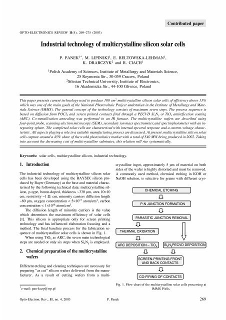
OPTO-ELECTRONICS REVIEW 11(4), 269–275 (2003) Industrial technology of multicrystalline silicon solar cells P. PANEK 1* , M. LIPINSKI 1 , E. BELTOWSKA-LEHMAN 1 , K. DRABCZYK 2 and R. CIACH 1 1 Polish Academy of Sciences, Institute of Metallurgy and Materials Science, 25 Reymonta Str., 30-059 Cracow, Poland 2 Silesian Technical University, Institute of Electronics, 16 Akademicka Str., 44-100 Gliwice, Poland This paper presents current technology used to produce 100 cm 2 multicrystalline silicon solar cells of efficiency above 13% which was one of the main goals of the National Photovoltaic Project undertaken in the Institute of Metallurgy and Materials Science (IMMS). The general concept of the technology consists of maximum seven steps. The process sequence is based on diffusion from POCl 3 and screen printed contacts fired through a PECVD Si xN y or TiO x antireflection coating (ARC). Co-metallisation annealing was performed in an IR furnace. The multicrystalline wafers are described using four-point probe, scanning electron microscopy (SEM), secondary ion mass spectrometer, and spectrophotometer with an integrating sphere. The completed solar cells are characterized with internal spectral response and a current-voltage characteristic. All aspects playing a role in a suitable manufacturing process are discussed. At present, multicrystalline silicon solar cells capture around a 45% share of the world photovoltaics market with a total of 540 MW being produced in 2002. Taking into account the decreasing cost of multicrystalline substrates, this relation will rise systematically. Keywords: solar cells, multicrystalline silicon, industrial technology. 1. Introduction The industrial technology of multicrystalline silicon solar cells has been developed using the BAYSIX silicon produced by Bayer (Germany) as the base and material characterised by the following technical data: multicrystalline silicon, p-type, boron-doped, thickness ~330 µm, area 10´10 cm, resistivity ~1 W cm, minority carriers diffusion length ~80 µm, oxygen concentration < 5´10 17 atom/cm 3 , carbon concentration < 1´10 18 atom/cm 3 . The diffusion length of minority carriers is the value which determines the maximum efficiency of solar cells [1]. This silicon is appropriate only for screen printing technology and has influenced elaboration focusing and a method. The final baseline process for the fabrication sequence of multicrystalline solar cells is shown in Fig. 1. When using TiO x as ARC, the seven main technological steps are needed or only six steps when Si xN y is employed. 2. Chemical preparation of the multicrystalline wafers Different etching and cleaning techniques are necessary for preparing “as cut” silicon wafers delivered from the manufacturer. As a result of cutting wafers from a multi- * e-mail: pan-kozy@wp.pl Contributed paper crystalline ingot, approximately 5 µm of material on both sides of the wafer is highly distorted and must be removed. A commonly used method, chemical etching in KOH or NaOH solution, is selective for grains with different crys- Fig. 1. Flow chart of the multicrystalline solar cells processing at IMMS PASs. Opto-Electron. Rev., 11, no. 4, 2003 P. Panek 269
- Page 2 and 3: Industrial technology of multicryst
- Page 4 and 5: Industrial technology of multicryst
- Page 6 and 7: Industrial technology of multicryst
- Page 8: Chair: H.C.Liu Co-chairs: S.D.Gunap
OPTO-ELECTRONICS REVIEW 11(4), 269–275 (2003)<br />
<strong>Industrial</strong> <strong>technology</strong> <strong>of</strong> <strong>multicrystalline</strong> <strong>silicon</strong> <strong>solar</strong> <strong>cells</strong><br />
P. PANEK 1* , M. LIPINSKI 1 , E. BELTOWSKA-LEHMAN 1 ,<br />
K. DRABCZYK 2 and R. CIACH 1<br />
1 Polish Academy <strong>of</strong> Sciences, Institute <strong>of</strong> Metallurgy and Materials Science,<br />
25 Reymonta Str., 30-059 Cracow, Poland<br />
2 Silesian Technical University, Institute <strong>of</strong> Electronics,<br />
16 Akademicka Str., 44-100 Gliwice, Poland<br />
This paper presents current <strong>technology</strong> used to produce 100 cm 2 <strong>multicrystalline</strong> <strong>silicon</strong> <strong>solar</strong> <strong>cells</strong> <strong>of</strong> efficiency above 13%<br />
which was one <strong>of</strong> the main goals <strong>of</strong> the National Photovoltaic Project undertaken in the Institute <strong>of</strong> Metallurgy and Materials<br />
Science (IMMS). The general concept <strong>of</strong> the <strong>technology</strong> consists <strong>of</strong> maximum seven steps. The process sequence is<br />
based on diffusion from POCl 3 and screen printed contacts fired through a PECVD Si xN y or TiO x antireflection coating<br />
(ARC). Co-metallisation annealing was performed in an IR furnace. The <strong>multicrystalline</strong> wafers are described using<br />
four-point probe, scanning electron microscopy (SEM), secondary ion mass spectrometer, and spectrophotometer with an integrating<br />
sphere. The completed <strong>solar</strong> <strong>cells</strong> are characterized with internal spectral response and a current-voltage characteristic.<br />
All aspects playing a role in a suitable manufacturing process are discussed. At present, <strong>multicrystalline</strong> <strong>silicon</strong> <strong>solar</strong><br />
<strong>cells</strong> capture around a 45% share <strong>of</strong> the world photovoltaics market with a total <strong>of</strong> 540 MW being produced in 2002. Taking<br />
into account the decreasing cost <strong>of</strong> <strong>multicrystalline</strong> substrates, this relation will rise systematically.<br />
Keywords: <strong>solar</strong> <strong>cells</strong>, <strong>multicrystalline</strong> <strong>silicon</strong>, industrial <strong>technology</strong>.<br />
1. Introduction<br />
The industrial <strong>technology</strong> <strong>of</strong> <strong>multicrystalline</strong> <strong>silicon</strong> <strong>solar</strong><br />
<strong>cells</strong> has been developed using the BAYSIX <strong>silicon</strong> produced<br />
by Bayer (Germany) as the base and material characterised<br />
by the following technical data: <strong>multicrystalline</strong> <strong>silicon</strong>,<br />
p-type, boron-doped, thickness ~330 µm, area 10´10<br />
cm, resistivity ~1 W cm, minority carriers diffusion length<br />
~80 µm, oxygen concentration < 5´10 17 atom/cm 3 , carbon<br />
concentration < 1´10 18 atom/cm 3 .<br />
The diffusion length <strong>of</strong> minority carriers is the value<br />
which determines the maximum efficiency <strong>of</strong> <strong>solar</strong> <strong>cells</strong><br />
[1]. This <strong>silicon</strong> is appropriate only for screen printing<br />
<strong>technology</strong> and has influenced elaboration focusing and a<br />
method. The final baseline process for the fabrication sequence<br />
<strong>of</strong> <strong>multicrystalline</strong> <strong>solar</strong> <strong>cells</strong> is shown in Fig. 1.<br />
When using TiO x as ARC, the seven main technological<br />
steps are needed or only six steps when Si xN y is employed.<br />
2. Chemical preparation <strong>of</strong> the <strong>multicrystalline</strong><br />
wafers<br />
Different etching and cleaning techniques are necessary for<br />
preparing “as cut” <strong>silicon</strong> wafers delivered from the manufacturer.<br />
As a result <strong>of</strong> cutting wafers from a multi-<br />
* e-mail: pan-kozy@wp.pl<br />
Contributed paper<br />
crystalline ingot, approximately 5 µm <strong>of</strong> material on both<br />
sides <strong>of</strong> the wafer is highly distorted and must be removed.<br />
A commonly used method, chemical etching in KOH or<br />
NaOH solution, is selective for grains with different crys-<br />
Fig. 1. Flow chart <strong>of</strong> the <strong>multicrystalline</strong> <strong>solar</strong> <strong>cells</strong> processing at<br />
IMMS PASs.<br />
Opto-Electron. Rev., 11, no. 4, 2003 P. Panek 269
<strong>Industrial</strong> <strong>technology</strong> <strong>of</strong> <strong>multicrystalline</strong> <strong>silicon</strong> <strong>solar</strong> <strong>cells</strong><br />
tallographic orientation on the surface and this causes discontinuities<br />
at the grain boundaries. However, this texturisation<br />
enhanced the light absorption but not to the same<br />
extent as in the case <strong>of</strong> (100) monocrystalline <strong>silicon</strong>. Some<br />
other proposals such as laser scribing, mechanical<br />
V-grooving or reactive ion etching (RIE) cannot be easy<br />
implemented in an industrial process which needs primarily<br />
high throughput at low cost. The acid etching, being an<br />
isotropic method, is still under investigation [2,3]. The<br />
well-prepared surfaces <strong>of</strong> the wafers must, as far as possible,<br />
be free <strong>of</strong> contaminants K + ions from the etching solution,<br />
heavy metals and organic impurities. The chemical<br />
procedure for cleaning the wafers before the donor doping<br />
process is given in Table 1.<br />
Following the etching and cleaning processes, the wafers<br />
were rinsed with 18 MWcm deionised water DIH 2Oin<br />
a cascade system as the final stage. During chemical treatment,<br />
the wafers were placed in a Teflon holder which<br />
could contain 25 slices.<br />
3. The p-n junction formation<br />
Emitter diffusion is one <strong>of</strong> the crucial steps in the manufacturing<br />
process <strong>of</strong> <strong>silicon</strong> <strong>solar</strong> <strong>cells</strong>. The donor source can<br />
be applied by techniques such as: screen printing, spray-on,<br />
spin-on or CVD (POCl 3) [4]. The emitter was generated at<br />
temperatures in the range 845–890°C for 40 min. in an<br />
open quartz tube using liquid POCl 3 as the doping source.<br />
This results is an emitter with a sheet resistance from 20<br />
W/� to 40 W/� as shown in Fig. 2. Sheet resistance was<br />
measured with automatic four-point probe which is the fundamental<br />
method used to control the diffusion process in<br />
industry. The selected wafers, measured at nine points, had<br />
emitters with homogeneity around 5% standard deviation.<br />
Table 1. Chemical processing applied to “as-cut” <strong>silicon</strong> wafers.<br />
Chemical process Chemical recipe<br />
This is acceptable taking into account that the wafer area is<br />
100 cm 2 and the diffusion furnace SD-3/158M has a quartz<br />
tube <strong>of</strong> 158 mm diameter. The diffusion pr<strong>of</strong>iles have been<br />
determined by secondary ion mass spectroscopy (SIMS)<br />
measurements.<br />
Table 2. The main electrical parameters <strong>of</strong> the <strong>solar</strong> <strong>cells</strong> in dependence<br />
on phosphorous concentration pr<strong>of</strong>ile adequate to<br />
shown in Fig. 2.<br />
Sheet resistance R s<br />
W/�<br />
I sc<br />
(A)<br />
V oc<br />
(V)<br />
FF<br />
E ff<br />
(%)<br />
20 2.749 0.561 0.748 11.53<br />
32 2.885 0.576 0.732 12.17<br />
40 2.979 0.578 0.731 12.60<br />
270 Opto-Electron. Rev., 11, no. 4, 2003 © 2003 COSiW SEP, Warsaw<br />
Time<br />
(min)<br />
Temperature<br />
(°C)<br />
Distorted layer removing 30% KOH 15 80<br />
Rinsing DIH 2O 25 25<br />
Rinsing IPA 15 25<br />
Texturisation IPA : 40%KOH : DIH 2O in vol. ratio 3:1:46 15 80<br />
Rinsing DIH 2O 25 25<br />
Neutralisation <strong>of</strong> potassium traces and<br />
metallic contamination removing<br />
95% H2SO4 :H2O in vol. ratio 1:1<br />
15 25<br />
Rinsing DIH2O 25 25<br />
Metallic contamination removing 2% HCl 15 25<br />
Rinsing DIH 2O 25 25<br />
Native oxide removing 10% HF 2 25<br />
Rinsing DIH 2O 25 25<br />
Fig. 2. Determined by SIMS phosphorous concentration pr<strong>of</strong>iles at<br />
diffusion time <strong>of</strong> 40 minutes in relation to diffusion temperature<br />
after process using POCl 3.
The <strong>cells</strong> obtained with the different emitters were analysed<br />
and, as can be seen in Table 2, the emitter with a<br />
sheet resistance in the range 40–50 W/� is optimal for<br />
screen-printing <strong>technology</strong>. The form <strong>of</strong> donor doping,<br />
shown in Fig. 2, obviously depends on temperature and<br />
time, but also on the diffusion <strong>technology</strong> realised with<br />
pre-oxidation before the pre-diffusion step. The second<br />
kind <strong>of</strong> diffusion technique was the formation <strong>of</strong> a n + /p<br />
structure using phosphorus-doped silica paste, marked by<br />
Soltech as 1. This was screen-printed onto wafers with a<br />
220-mesh screen and after drying the wafers were placed in<br />
an IR furnace where the diffusion occurs in 5 min at a temperature<br />
above 900°C [5]. Phosphorus from paste diffuses<br />
into the desired front side <strong>of</strong> the wafer. The average results<br />
for 100 cm 2 <strong>solar</strong> <strong>cells</strong> with emitter formed with 1 paste,<br />
covered TiO x, have reached the following value: I sc = 2.589<br />
A, V oc = 0.599 V, FF = 0.74 and E ff = 11.5% what is below<br />
the parameters characterised by <strong>solar</strong> <strong>cells</strong> after processing<br />
with POCl 3 as it can be seen in Tables 3 and 5.<br />
4. Parasitic junction removal and chemical<br />
etching<br />
After diffusion from POCl 3, the wafers are covered by<br />
phosphorus-silicate glass xSiO 2 � yP 2O 5 and have donor-doping<br />
layer on both sides and edges. At first, the parasitic<br />
junction was removed by means <strong>of</strong> a special Teflon<br />
clamp in which the <strong>silicon</strong> wafers previously immersed in a<br />
glycerine-water solution were stacked surface by surface<br />
with EVA foil separation. Next, the clamp was immersed<br />
in 65%HNO 3:40%HF:80%CH 3COOH solution in the volume<br />
ratio 5:3:3 for 1 min. followed by rinsing in DI H 2O.<br />
Then xSiO 2 � yP 2O 5 was removed by immersion in a bath<br />
<strong>of</strong> 10% HF for 2 min. Finishing all wet chemical baths, the<br />
wafers were dried in a spin-drier with the highly purified<br />
air. It is more difficult to obtain a clean and non-wetting<br />
wafer surface by chemical etching after using 1 paste and<br />
the phosphorus glass layer has to be removed in 25% HF<br />
using an ultrasonic cleaner.<br />
5. Passivation process<br />
Surface passivation was achieved by the growth <strong>of</strong> a thin,<br />
invisible passivating oxide SiO 2 at a temperature <strong>of</strong> 800°C<br />
for 15 min. in a controlled O 2 and N 2 atmosphere. Increasing<br />
the time did not increase the short circuit current<br />
I sc significantly and the shorter did not give an expected<br />
improvement as it can be seen in Fig. 3 and Table 3.<br />
The oxygen and nitrogen used for the thermal annealing<br />
and diffusion processes were dried to a dryness <strong>of</strong> 0.005<br />
mg/l and purified with 5A Molecular Sieves system to remove<br />
impurities that have effective molecular diameter <strong>of</strong><br />
less than 5 angstroms.<br />
The improvement in the cell efficiency depends among<br />
others on the open circuit voltage V oc and for maximising<br />
the V oc it is very important to reduce the recombination ve-<br />
locity at the surface, under contacts and in the bulk. A thermal<br />
oxide is effective in reducing the surface recombination<br />
velocity whilst bulk passivation is possible by, for example,<br />
<strong>silicon</strong> nitride.<br />
6. Antireflection coatings deposition<br />
Contributed paper<br />
Table 3. The parameters current-voltage characteristic <strong>solar</strong> <strong>cells</strong><br />
realised in <strong>technology</strong> including TiO x as ARC with and without<br />
passivated layer SiO 2 grows for the time 15 min.<br />
Solar cell I sc [A] V oc [V] FF E ff [%]<br />
Without SiO 2 2.461 0.545 0.737 9.91<br />
With SiO 2 2.903 0.583 0.736 12.47<br />
Change [%] +17.9 +6.9 0 +25.8<br />
Fig. 3. Short circuit current <strong>of</strong> <strong>solar</strong> <strong>cells</strong> with TiO x for different dry<br />
oxidation time.<br />
The Si surface reflects 35–50% <strong>of</strong> the light, depending upon<br />
its wavelength in the range 400–1100 nm on which the photovoltaic<br />
conversion depends. Obtaining the lower reflective<br />
surface on the <strong>multicrystalline</strong> <strong>silicon</strong> <strong>solar</strong> cell is difficult because<br />
<strong>of</strong> the presence <strong>of</strong> randomly oriented crystallites. An<br />
improvement can be only achieved by forming an antireflection<br />
coating (ARC) to reduce the <strong>solar</strong> cell reflection to below<br />
10% [1]. In industry two antireflection coatings are widely<br />
applied: titanium oxide TiO x and <strong>silicon</strong> nitride Si xN y. Both<br />
were deposited before contacts were screen-printed. It is very<br />
important for soldering <strong>of</strong> the <strong>solar</strong> <strong>cells</strong> because before connecting<br />
them in a module there is no necessity to remove<br />
ARC from the front busbar electrode. The Si xN y was deposited<br />
by plasma enhanced chemical vapour deposition<br />
(PECVD). It has following advantages [6]:<br />
by changing the deposition conditions: power, temperature,<br />
pressure and NH 3/SiH 4 ratio Si xN y can be obtained<br />
with the required optical and material parameters best<br />
suited for <strong>solar</strong> <strong>cells</strong>. Specifically a refractive index <strong>of</strong><br />
1.9 for 600 nm wavelength, extinction coefficient above<br />
400 nm wavelength sharply decreasing to 0, control <strong>of</strong><br />
hydrogen content and a positive charge present on the<br />
<strong>solar</strong> cell surface,<br />
Opto-Electron. Rev., 11, no. 4, 2003 P. Panek 271
<strong>Industrial</strong> <strong>technology</strong> <strong>of</strong> <strong>multicrystalline</strong> <strong>silicon</strong> <strong>solar</strong> <strong>cells</strong><br />
the Si xN y film deposition has a role as a bulk and surface<br />
passivator as well as providing the antireflection<br />
coating,<br />
it gives possibilities <strong>of</strong> simultaneous firing <strong>of</strong> front and<br />
back contacts,<br />
it reduces the production process to six steps as it allows<br />
the thermal oxidation process to be omitted.<br />
The TiO x layers have excellent optical properties as<br />
ARCs for <strong>multicrystalline</strong> <strong>solar</strong> <strong>cells</strong>. Namely, the refractive<br />
index <strong>of</strong> about 2.38 at a wavelength <strong>of</strong> 600 nm and an<br />
extinction coefficient remaining near zero under the wavelength<br />
<strong>of</strong> 400 nm [7]. A TiO x film produced at the temperature<br />
below 300°C is primarily amorphous which makes the<br />
metallisation <strong>of</strong> the front contacts easier. According to the<br />
flow chart presented in Fig. 1, after dry passivation, the<br />
TiO x was deposited by spraying at 280°C with tetraethylorthotitanat<br />
(C 2H 5O) 4Ti using purified air as a carrier gas.<br />
Figure 4 shows internal quantum efficiency and reflectance<br />
for <strong>solar</strong> cell done with TiO x.<br />
Fig. 4. Internal quantum efficiency (IQE) and reflectance for <strong>solar</strong><br />
cell with SiO 2 passivated layer and ARC with TiO x.<br />
7. Screen-printing front and back contacts<br />
The screen-printing process is very simple and commonly<br />
used in industrial production. A few types <strong>of</strong> the<br />
photovoltaic pastes were tested and eventually silver<br />
paste PV145, manufactured by Du Pont, was used on the<br />
front and aluminium T-14002A, produced by Engelhard,<br />
was used on the back and were printed using 330 mesh<br />
screens. The front paths designed on the screen were 120<br />
µm wide with 3.3 mm spacing which gives, together with<br />
the two main collection busbars 1 mm wide, a 5.6% front<br />
shadow. Back contact covering the full rear surface was<br />
deposited with pure Al paste. The two collection back<br />
busbarr contacts were printed with a Polish silver paste<br />
P-124 containing 3% aluminium. The collection back<br />
bur contacts must not have a greater quantity <strong>of</strong> aluminium<br />
in the paste because soldering for interconnecting<br />
<strong>cells</strong> would be impossible.<br />
8. Co-firing <strong>of</strong> metal contacts<br />
Table 4. Parameters set for the co-firing process in the IR furnace.<br />
I zone<br />
temperature (°C)<br />
II zone<br />
temperature (°C)<br />
Fig. 5. Schematic structure <strong>of</strong> <strong>solar</strong> cell with TiO x layer as ARC. If<br />
the <strong>silicon</strong> nitride is used as ARC the layer indicated as<br />
“passivation oxide” is not present.<br />
A conveyor belt IR furnace with fitted tungsten filament<br />
lamps, heating the top and bottom <strong>of</strong> the belt, was used for<br />
simultaneous metallisation for the front and back electrodes<br />
[5]. The three following heating zones are 18 cm, 36 cm<br />
and 18 cm long and the belt speed is in the range 50–200<br />
cm/min. The technical parameters <strong>of</strong> the annealing treatment<br />
are given in Table 4 while the thermal pr<strong>of</strong>iles are<br />
shown in Fig. 6.<br />
After drying in air at 150°C the printed pastes were<br />
co-fired in the IR belt furnace. The wafers during<br />
metallisation are at a temperature above 577°C for about 13<br />
seconds and obviously this process can be classified as<br />
rapid thermal annealing. This process can be qualified by<br />
the current-voltage characteristic parameters: fill factor, series<br />
and shunt resistance [1]. This IR annealing process<br />
gives an acceptable value <strong>of</strong> 10 mW for the series resistance<br />
and a shunt resistance <strong>of</strong> 0.035 kW resulting in a fill<br />
factor <strong>of</strong> 0.74.<br />
To obtain a good back surface field (BSF) a thick aluminium<br />
layer ~20 µm is required but it cause the wafer to<br />
be bent after firing due to the different expansion coefficients<br />
<strong>of</strong> Si and Al. The degree <strong>of</strong> curvature depends on the<br />
thickness <strong>of</strong> the wafer and the 200 µm is the limit before<br />
the degree <strong>of</strong> curvature makes the <strong>cells</strong> interconnection in a<br />
III zone<br />
temperature (°C)<br />
Belt speed<br />
(cm/min)<br />
Solar <strong>cells</strong> with TiO x 550 550 880 160<br />
Solar <strong>cells</strong> with Si xN y 550 750 880 200<br />
272 Opto-Electron. Rev., 11, no. 4, 2003 © 2003 COSiW SEP, Warsaw
Fig. 6. Temperature pr<strong>of</strong>iles vs. elapsed time for <strong>solar</strong> cell<br />
metallisation in the IR furnace.<br />
standard module impossible. The Al layer not only produces<br />
a BSF but also helps to passivate defects in the bulk<br />
Si, especially when <strong>silicon</strong> nitride is applied [8].<br />
9. Measurements and results<br />
The illuminated I-V parameters were measured under standard<br />
simulated AM 1.5 (100 mW/cm 2 ) radiation and an example<br />
report is shown in Fig. 8. A reference cell was calibrated<br />
at IMEC, Belgium. To confirm the repeatability <strong>of</strong><br />
the <strong>technology</strong> a few experimental <strong>solar</strong> <strong>cells</strong> series were<br />
produced following the procedures given in Fig. 1. Two<br />
Contributed paper<br />
Fig. 7. SEM micrograph <strong>of</strong> cross-section <strong>multicrystalline</strong> <strong>solar</strong> cell<br />
after co-firing <strong>of</strong> metal contacts in IR furnace. The Aluminium<br />
back contact is 30-µm thick. The front electrode grid line is 160-µm<br />
wide and 25-µm high. The cell thickness is 290 µm.<br />
were selected as examples; one with TiO x and second with<br />
Si xN y. The results are presented in Figs. 9 and 10 showing<br />
the Gauss distribution and in Table 4.<br />
As it can be seen good average short circuit current<br />
density, around 30 mA/cm 2 , and the required photovoltaic<br />
conversion efficiency above 13% were obtained. In the<br />
case <strong>of</strong> <strong>cells</strong> with Si xN y, the best I sc around 3.2 A and noticeable<br />
voltage 600 mV has been obtained thanks to excellent<br />
surface and bulk passivation by a hydrogenation process<br />
at temperatures <strong>of</strong> 600–800°C. An average value <strong>of</strong> 10<br />
mW for the series resistance and 0.035 kW for the shunt re-<br />
Fig. 8. The measured I-V report for <strong>multicrystalline</strong> <strong>silicon</strong> <strong>solar</strong> cell with Si xN y. The numerical fitting was realized by applying double<br />
exponential model containing seven modelling parameters [9].<br />
Opto-Electron. Rev., 11, no. 4, 2003 P. Panek 273
<strong>Industrial</strong> <strong>technology</strong> <strong>of</strong> <strong>multicrystalline</strong> <strong>silicon</strong> <strong>solar</strong> <strong>cells</strong><br />
Fig. 9. Gauss distribution <strong>of</strong> efficiency for series 200 <strong>solar</strong> <strong>cells</strong><br />
with TiO x.<br />
sistance is good and give a fill factor <strong>of</strong> 0.74. The <strong>silicon</strong><br />
nitride allows the omission <strong>of</strong> the dry oxidation process and<br />
reduces the main fabrication steps to six. This would appear<br />
to be particularly attractive since there are no other industrial<br />
alternatives [10].<br />
Photovoltaic cell production grew by 35% in 2002 year<br />
with a total <strong>of</strong> 540 MW being produced and <strong>multicrystalline</strong><br />
<strong>silicon</strong> <strong>solar</strong> <strong>cells</strong> have captured around 45% <strong>of</strong> the<br />
world market [11].<br />
10. Conclusions<br />
A simple industrial procedure for manufacturing high<br />
efficiency <strong>solar</strong> <strong>cells</strong> on 100-cm 2 <strong>multicrystalline</strong> <strong>silicon</strong><br />
has been developed.<br />
Multicrystalline <strong>silicon</strong> <strong>solar</strong> <strong>cells</strong> with an average cell<br />
efficiency above 12% with TiO x and 13% with Si xN y<br />
have been manufactured.<br />
Fig. 10. Gauss distribution <strong>of</strong> efficiency for series 40 <strong>solar</strong> <strong>cells</strong><br />
with Si xN y.<br />
The <strong>technology</strong> including TiO x as antireflection coating<br />
can be easy transferred to a production line without incurring<br />
high costs.<br />
The <strong>technology</strong> for manufacturing <strong>multicrystalline</strong> <strong>silicon</strong><br />
<strong>solar</strong> <strong>cells</strong> with Si xN y requires purchase <strong>of</strong> an industrial<br />
PECVD device for Si xN y deposition with a minimum<br />
throughput 500 <strong>silicon</strong> slices per hour. The use <strong>of</strong><br />
this device reduced the process steps to six and opens<br />
new scientific areas.<br />
Acknowledgements<br />
This work was supported by the Polish State Committee for<br />
Scientific Research (KBN) under Project No. 05/T11/98.<br />
The authors would like to thank E. Bielañska from IMMS<br />
PAS in Cracow for the SEM investigation and H.<br />
Czternastek from University <strong>of</strong> Mining and Metallurgy in<br />
Cracow for reflectance measurements. We gratefully acknowledge<br />
J. Szlufcik from IMEC for his valuable contributions<br />
to this work.<br />
Table 5. The average values calculated from Gauss distribution <strong>of</strong> the main parameters current-voltage (I-V) characteristic for 200<br />
pieces <strong>solar</strong> <strong>cells</strong> with TiO x and 40 pieces <strong>solar</strong> <strong>cells</strong> with Si xN y and the best <strong>multicrystalline</strong> 100 cm 2 <strong>solar</strong> <strong>cells</strong> in a particular series.<br />
Average value<br />
I sc (A) V oc (V) FF E ff (%)<br />
Solar <strong>cells</strong> with TiO x 2.960 0.575 0.722 12.29<br />
Solar <strong>cells</strong> with Si x N y 3.058 0.594 0.726 13.19<br />
Best value<br />
I sc (A) V oc (V) FF E ff (%)<br />
Solar <strong>cells</strong> with TiO x 3.009 0.581 0.749 13.09<br />
Solar <strong>cells</strong> with Si x N y 3.177 0.600 0.721 13.70<br />
274 Opto-Electron. Rev., 11, no. 3, 2003 © 2003 COSiW SEP, Warsaw
References<br />
1. A. Goetzberger, J. Knobloch, and B. Voss, Crystalline Silicon<br />
Solar Cells, John Wiley & Sons, Chichester, England, 1998.<br />
2. M. Lipinski, P. Panek, Z. Swi¹tek, E. Beltowska, and R.<br />
Ciach, “Double porous <strong>silicon</strong> layer on multi-crystalline Si<br />
for photovoltaic application”, Solar Energy Materials & Solar<br />
Cells 72, 271–276 (2002).<br />
3. V.Y Yerokhov, M. Lipinski, R. Ciach, H. Nagel, A.<br />
Mylyanych, and P. Panek, “Cost-effective methods <strong>of</strong> texturing<br />
for <strong>silicon</strong> <strong>solar</strong> <strong>cells</strong>”, Solar Energy Materials & Solar<br />
Cells 72, 291–298 (2002).<br />
4. K. Waczynski, K. Drabczyk, M. Lipinski, and P. Panek,<br />
“Doping <strong>technology</strong> using silica glasses investigation <strong>of</strong> the<br />
emitter layer <strong>of</strong> the <strong>silicon</strong> <strong>solar</strong> cell”, Proc. Int. Conf.<br />
IMAPS XXVI, 221–224 (2002).<br />
5. P. Panek, M. Lipinski, R. Ciach, K. Drabczyk, and E.<br />
Bielanska, “The infrared processing in <strong>multicrystalline</strong> <strong>silicon</strong><br />
<strong>solar</strong> cell low-cost <strong>technology</strong>”, Solar Energy Materials<br />
& Solar Cells 76, 529–534 (2003).<br />
Contributed paper<br />
6. F. Duerinckx, J. Szlufcik, A. Ziebakowski, J. Nijs, and R.<br />
Mertens, “Simple and efficient screen printing process for<br />
<strong>multicrystalline</strong> <strong>silicon</strong> <strong>solar</strong> <strong>cells</strong> based on firing through<br />
<strong>silicon</strong> nitride”, Proc. European Photovoltaic Solar Energy<br />
Conf. 14, 792–795 (1997).<br />
7. B.S. Richards, J.E. Cotter, C.B. Honsberg, and S.R.<br />
Wenham, “Novel uses <strong>of</strong> TiO 2 in crystalline <strong>silicon</strong> <strong>solar</strong><br />
<strong>cells</strong>”, Proc. IEEE 28, 375–378 (2000).<br />
8. S. Bowden, F. Duerinckx, J. Szlufcik, and J. Nijs, “Rear<br />
passivation <strong>of</strong> thin <strong>multicrystalline</strong> <strong>silicon</strong> <strong>solar</strong> <strong>cells</strong>”,<br />
Opto-Electron. Rev. 8, 307–310 (2000).<br />
9. T. Zdanowicz, “The interactive computer program to fit I-V<br />
curves <strong>of</strong> <strong>solar</strong> <strong>cells</strong>”, Proc. European Photovoltaic Solar<br />
Energy Conf. 12, 1311–1314 (1994).<br />
10. J. Szlufcik, F. Duerinckx, J. Horzel, E. van Kerschaver, R.<br />
Einhaus, K. De Clercq, H. Dekkers, and J. Nijs, “Advanced<br />
concept <strong>of</strong> industrial technologies <strong>of</strong> crystalline <strong>silicon</strong> <strong>solar</strong><br />
<strong>cells</strong>”, Opto-Electron. Rev. 8, 299–306 (2000).<br />
11. Information in “News” <strong>of</strong> Renewable Energy World 8, 12<br />
(2003).<br />
Opto-Electron. Rev., 11, no. 4, 2003 P. Panek 275
Chair: H.C.Liu<br />
Co-chairs: S.D.Gunapala & H.Schneider<br />
Advisory committee:<br />
Sumith Bandara – JPL USA<br />
Pallab Bhattacharya – U. Michigan USA<br />
Ph. Bois – Thales France<br />
Gail Brown – AFRL USA<br />
Anna Carbone – Polito Italy<br />
Dave Cardimona – AFRL USA<br />
E. Finkman – Technion Israel<br />
Bernhard Hirschauer – Acreo Sweden<br />
Vincent Larochelle – DRDC Canada<br />
Paul LeVan – AFRL USA<br />
Barbara McQuiston – QWIPTech USA<br />
Unil Perera – GSU USA<br />
Gabby Sarusi – Elop Israel<br />
Meimei Tidrow – BMDO USA<br />
Benny Toomarian – JPL USA<br />
Workshop coordinator:<br />
Tania Oogarah, Tel: 613 993–7116,<br />
Fax: 613 990 0202,<br />
E-mail: Tania.Oogarah@nrc.ca<br />
QWIP2004<br />
International Workshop on Quantum Well<br />
Infrared Photodetectors<br />
August 9–12, 2004<br />
The Canadian Rockies<br />
Delta Lodge at Kananaskis, Alberta<br />
Introduction:<br />
This workshop is the third one <strong>of</strong> the series following<br />
QWIP2000 in Dana Point (USA) and QWIP2002 in<br />
Torino (Italy). QWIP is now a <strong>technology</strong> for infrared<br />
imaging, after rapid development in the past 15 years.<br />
It is also because <strong>of</strong> this rapid advance, some areas are<br />
not yet completely resolved and potentials are not fully<br />
exploited. The primary goal <strong>of</strong> this workshop is to<br />
gather all the experts in the QWIP R&D, government<br />
sponsors, industrial engineers, instrument technologists,<br />
end users, etc., and then discuss the current issues,<br />
formulate directions, and establish collaborations.<br />
Scope:<br />
QWIP physics; for example, advanced or fully<br />
quantum mechanical QWIP model, realistic grating<br />
and optical coupler model, solutions to the slow<br />
response in low temperature and low background<br />
QWIP <strong>technology</strong>, for example, multicolor and<br />
multiband arrays<br />
QWIP applications, for example, military,<br />
medical/health, and commercial<br />
QWIP novel direction, for example, ultrahigh speed,<br />
two-photon response<br />
Related new approaches, for example quantum dots<br />
and other materials<br />
Related devices<br />
Format:<br />
The workshop is intended to provide a forum where<br />
ample time is allotted for presentation and discussion.<br />
The number <strong>of</strong> participants is limited to facilitate this<br />
goal. A good/basic prior knowledge <strong>of</strong> QWIP is<br />
assumed.<br />
Tentative dates:<br />
Abstract deadline: April 23, 2004<br />
Notification <strong>of</strong> acceptance/rejection: May 14, 2004<br />
Registration: June 23, 2004<br />
276 Opto-Electron. Rev., 11, no. 4, 2003 © 2003 COSiW SEP, Warsaw


