SCAN90004 4-Channel LVDS Buffer/Repeater with Pre-Emphasis ...
SCAN90004 4-Channel LVDS Buffer/Repeater with Pre-Emphasis ...
SCAN90004 4-Channel LVDS Buffer/Repeater with Pre-Emphasis ...

Create successful ePaper yourself
Turn your PDF publications into a flip-book with our unique Google optimized e-Paper software.
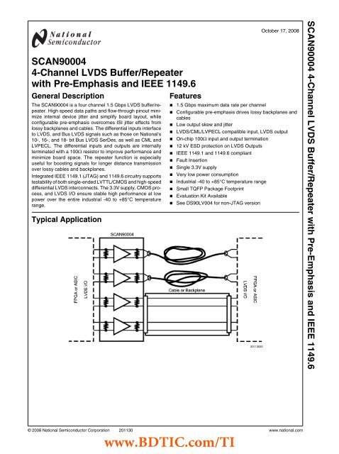
<strong>SCAN90004</strong>4-<strong>Channel</strong> <strong>LVDS</strong> <strong>Buffer</strong>/<strong>Repeater</strong><strong>with</strong> <strong>Pre</strong>-<strong>Emphasis</strong> and IEEE 1149.6General DescriptionThe <strong>SCAN90004</strong> is a four channel 1.5 Gbps <strong>LVDS</strong> buffer/repeater.High speed data paths and flow-through pinout minimizeinternal device jitter and simplify board layout, whileconfigurable pre-emphasis overcomes ISI jitter effects fromlossy backplanes and cables. The differential inputs interfaceto <strong>LVDS</strong>, and Bus <strong>LVDS</strong> signals such as those on National's10-, 16-, and 18- bit Bus <strong>LVDS</strong> SerDes, as well as CML andLVPECL. The differential inputs and outputs are internallyterminated <strong>with</strong> a 100Ω resistor to improve performance andminimize board space. The repeater function is especiallyuseful for boosting signals for longer distance transmissionover lossy cables and backplanes.Integrated IEEE 1149.1 (JTAG) and 1149.6 circuitry supportstestability of both single-ended LVTTL/CMOS and high-speeddifferential <strong>LVDS</strong> interconnects. The 3.3V supply, CMOS process,and <strong>LVDS</strong> I/O ensure stable high performance at lowpower over the entire industrial -40 to +85°C temperaturerange.Typical ApplicationFeaturesOctober 17, 2008■ 1.5 Gbps maximum data rate per channel■ Configurable pre-emphasis drives lossy backplanes andcables■ Low output skew and jitter■ <strong>LVDS</strong>/CML/LVPECL compatible input, <strong>LVDS</strong> output■ On-chip 100Ω input and output termination■ 12 kV ESD protection on <strong>LVDS</strong> Outputs■ IEEE 1149.1 and 1149.6 compliant■ Fault Insertion■ Single 3.3V supply■ Very low power consumption■ Industrial -40 to +85°C temperature range■ Small TQFP Package Footprint■ Evaluation Kit Available■ See DS90LV004 for non-JTAG version20113020<strong>SCAN90004</strong> 4-<strong>Channel</strong> <strong>LVDS</strong> <strong>Buffer</strong>/<strong>Repeater</strong> <strong>with</strong> <strong>Pre</strong>-<strong>Emphasis</strong> and IEEE 1149.6© 2008 National Semiconductor Corporation 201130 www.national.comwww.BDTIC.com/TI
BDTIC 半 导 体 事 业 部www.BDTIC.com/NSCNSC 国 家 半 导 体 公 司 产 品 部 门www.BDTIC.com/TI
<strong>SCAN90004</strong>Block and Connection DiagramsPinout - Top View2011300220113001<strong>SCAN90004</strong> Block Diagramwww.national.com 2www.BDTIC.com/TI
Pin DescriptionsPinNameDIFFERENTIAL INPUTSIN0+IN0−IN1+IN1−IN2+IN2−IN3+IN3−DIFFERENTIAL OUTPUTSOUT0+OUT0−OUT1+OUT1−OUT2+OUT2−OUT3+OUT3-TQFP PinNumber13141516192021224847464542414039DIGITAL CONTROL INTERFACEI/O, TypeDescriptionI, <strong>LVDS</strong> <strong>Channel</strong> 0 inverting and non-inverting differential inputs.I, <strong>LVDS</strong> <strong>Channel</strong> 1 inverting and non-inverting differential inputs.I, <strong>LVDS</strong> <strong>Channel</strong> 2 inverting and non-inverting differential inputs.I, <strong>LVDS</strong> <strong>Channel</strong> 3 inverting and non-inverting differential inputs.O, <strong>LVDS</strong> <strong>Channel</strong> 0 inverting and non-inverting differential outputs. (Note 1)O, <strong>LVDS</strong> <strong>Channel</strong> 1 inverting and non-inverting differential outputs. (Note 1)O, <strong>LVDS</strong> <strong>Channel</strong> 2 inverting and non-inverting differential outputs. (Note 1)O, <strong>LVDS</strong> <strong>Channel</strong> 3 inverting and non-inverting differential outputs. (Note 1)PWDN 12 I, LVTTL A logic low at PWDN activates the hardware power down mode.PEM0PEM112I, LVTTL <strong>Pre</strong>-emphasis Control Inputs (affects all <strong>Channel</strong>s)TDI 34 I, LVTTL Test Data Input to support IEEE 1149.1 featuresTDO 35 O, LVTTL Test Data Output to support IEEE 1149.1 featuresTMS 27 I, LVTTL Test Mode Select to support IEEE 1149.1 featuresTCK 26 I, LVTTL Test Clock to support IEEE 1149.1 featuresTRST 25 I, LVTTL Test Reset to support IEEE 1149.1 featuresPOWERV DD 3, 4, 5, 7, 10, 11, 28, 29, 32, 33 I, Power V DD = 3.3V, ±5%GND 8, 9, 17, 18, 23, 24, 37, 38, 43, 44 I, Power GroundN/C 6, 30, 31, 36 No Connect<strong>SCAN90004</strong>Note 1: The <strong>LVDS</strong> outputs do not support a multidrop (B<strong>LVDS</strong>) environment. The <strong>LVDS</strong> output characteristics of the <strong>SCAN90004</strong> device have been optimizedfor point-to-point backplane and cable applications.3 www.national.comwww.BDTIC.com/TI
<strong>SCAN90004</strong>Absolute Maximum Ratings (Note 2)Supply Voltage (V DD )CMOS Input Voltage<strong>LVDS</strong> Input Voltage (Note 3)<strong>LVDS</strong> Output Voltage−0.3V to +4.0V-0.3V to (V DD +0.3V)-0.3V to (V DD +0.3V)-0.3V to (V DD +0.3V)<strong>LVDS</strong> Output Short Circuit Current+40 mAJunction Temperature+150°CStorage Temperature−65°C to +150°CLead Temperature (Solder, 4sec) 260°CMax Pkg Power Capacity @ 25°C 1.64WThermal Resistance (θ JA )76°C/WPackage Derating above +25°C13.2mW/°CESD Last Passing Voltage (<strong>LVDS</strong> output pins)HBM, 1.5kΩ, 100pFEIAJ, 0Ω, 200pF12kV250VESD Last Passing Voltage (All other pins)HBM, 1.5kΩ, 100pFEIAJ, 0Ω, 200pFRecommended OperatingConditions8kV250VSupply Voltage (V CC ) 3.15V to 3.45VInput Voltage (V I ) (Note 3)Output Voltage (V O )Operating Temperature (T A )Industrial0V to V CC0V to V CC−40°C to +85°CNote 2: Absolute maximum ratings are those values beyond which damageto the device may occur. The databook specifications should be met, <strong>with</strong>outexception, to ensure that the system design is reliable over its power supply,temperature, and output/input loading variables. National does notrecommend operation of products outside of recommended operationconditions.Note 3: V ID max < 2.4VElectrical CharacteristicsOver recommended operating supply and temperature ranges unless other specified.Symbol Parameter Conditions MinLVTTL DC SPECIFICATIONS (PWDN, PEM0, PEM1, TDI, TDO, TCK, TMS, TRST)Typ(Note 4)V IH High Level Input Voltage 2.0 V DD VV IL Low Level Input Voltage GND 0.8 VI IH High Level Input Current V IN = V DD = V DDMAX −10 +10 µAI IL Low Level Input Current V IN = V SS , V DD = V DDMAX −10 +10 µAI ILR Low Level Input Current TDI, TMS, TRST -40 -200 µAC IN1 Input Capacitance Any Digital Input Pin to V SS 3.5 pFC OUT1 Output Capacitance Any Digital Output Pin to V SS 5.5 pFV CL Input Clamp Voltage I CL = −18 mA −1.5 −0.8 VV OHV OLHigh Level Output Voltage(TDO)Low Level Output Voltage(TDO)MaxI OH = −12 mA, V DD = 3.15 V 2.4 VI OH = −100 µA, V DD = 3.15 V V DD -0.2 VI OL = 12 mA, V DD = 3.15 V 0.5 VI OL = 100 µA, V DD = 3.15 V 0.2 VI OS Output Short Circuit Current TDO −15 −125 mAI OZ Output TRI-STATE Current TDO −10 +10 µA<strong>LVDS</strong> INPUT DC SPECIFICATIONS (INn±)V THV TLDifferential Input High Threshold(Note 5)Differential Input Low Threshold(Note 5)V CM = 0.8V to 3.4V,V DD = 3.45VV CM = 0.8V to 3.4V,V DD = 3.45VUnits0 100 mV−100 0 mVV ID Differential Input Voltage V CM = 0.8V to 3.4V, V DD = 3.45V 100 2400 mVV CMR Common Mode Voltage Range V ID = 150 mV, V DD = 3.45V 0.05 3.40 VC IN2 Input Capacitance IN+ or IN− to V SS 5.2 pFI IN Input Current V IN = 3.45V, V DD = V DDMAX −10 +10 µAV IN = 0V, V DD = V DDMAX −10 +10 µAwww.national.com 4www.BDTIC.com/TI
Symbol Parameter Conditions Min<strong>LVDS</strong> OUTPUT DC SPECIFICATIONS (OUTn±)V ODΔV ODDifferential Output Voltage,0% <strong>Pre</strong>-emphasis (Note 5)Change in V OD betweenComplementary StatesR L = 100Ω external resistor between OUT+ andOUT−Typ(Note 4)MaxUnits250 500 600 mV-35 35 mVV OS Offset Voltage (Note 6) 1.05 1.18 1.475 VΔV OSChange in V OS betweenComplementary States-35 35 mVI OS Output Short Circuit Current OUT+ or OUT− Short to GND −60 −90 mAC OUT2 Output Capacitance OUT+ or OUT− to GND when TRI-STATE 5.5 pFSUPPLY CURRENT (Static)I CC Supply Current All inputs and outputs enabled and active,I CCZSupply Current - Power DownModeSWITCHING CHARACTERISTICS—<strong>LVDS</strong> OUTPUTSt LHTt HLTt PLHDt PHLDDifferential Low to HighTransition TimeDifferential High to LowTransition TimeDifferential Low to HighPropagation DelayDifferential High to LowPropagation Delayterminated <strong>with</strong> external differential load of 100Ωbetween OUT+ and OUT-, 0% pre-emphasisPWDN = L, 0% pre-emphasisUse an alternating 1 and 0 pattern at 200 Mb/s,measure between 20% and 80% of V OD . (Note11)Use an alternating 1 and 0 pattern at 200 Mb/s,measure at 50% V OD between input to output.117 140 mA2.7 6 mA210 300 ps210 300 ps2.0 3.2 ns2.0 3.2 nst SKD1 Pulse Skew |t PLHD –t PHLD | (Note 11) 25 80 pst SKCC Output <strong>Channel</strong> to <strong>Channel</strong> Skew Difference in propagation delay (t PLHD or t PHLD )among all output channels. (Note 11)t SKP Part to Part Skew (Note 11) Common edge, parts at same temp and V CC (Note11)t JITJitter (0% <strong>Pre</strong>-emphasis)(Note 7)50 125 ps1.1 nsRJ - Alternating 1 and 0 at 750 MHz (Note 8) 1.1 1.5 psrmsDJ - K28.5 Pattern, 1.5 Gbps (Note 9) 43 62 psp-pTJ - PRBS 2 23 -1 Pattern, 1.5 Gbps (Note 10) 35 85 psp-pt ON <strong>LVDS</strong> Output Enable Time Time from PWDN to OUT± change from TRI-STATE to active.t OFF <strong>LVDS</strong> Output Disable Time Time from PWDN to OUT± change from active toTRI-STATE.300 ns12 ns<strong>SCAN90004</strong>5 www.national.comwww.BDTIC.com/TI
<strong>SCAN90004</strong>Symbol Parameter Conditions MinSWITCHING CHARACTERISTICS—SCAN FEATURESTyp(Note 4)f MAX Maximum TCK Clock Frequency R L = 500Ω,25.0 MHzt S TDI to TCK, H or L C L = 35 pF3.0 nst H TDI to TCK, H or L 0.5 nst S TMS to TCK, H or L 2.5 nst H TMS to TCK, H or L 0.5 nst W TCK Pulse Width, H or L 10.0 nst W TRST Pulse Width, L 2.5 nst REC Recovery Time, TRST to TCK 1.0 nsMaxUnitsNote 4: Typical parameters are measured at V DD = 3.3V, T A = 25°C. They are for reference purposes, and are not production-tested.Note 5: Differential output voltage V OD is defined as ABS(OUT+–OUT−). Differential input voltage V ID is defined as ABS(IN+–IN−).Note 6: Output offset voltage V OS is defined as the average of the <strong>LVDS</strong> single-ended output voltages at logic high and logic low states.Note 7: Jitter is not production tested, but guaranteed through characterization on a sample basis.Note 8: Random Jitter, or RJ, is measured RMS <strong>with</strong> a histogram including 1500 histogram window hits. The input voltage = V ID = 500mV, 50% duty cycle at750MHz, t r = t f = 50ps (20% to 80%).Note 9: Deterministic Jitter, or DJ, is measured to a histogram mean <strong>with</strong> a sample size of 350 hits. The input voltage = V ID = 500mV, K28.5 pattern at 1.5 Gbps,t r = t f = 50ps (20% to 80%). The K28.5 pattern is repeating bit streams of (0011111010 1100000101).Note 10: Total Jitter, or TJ, is measured peak to peak <strong>with</strong> a histogram including 3500 window hits. Stimulus and fixture jitter has been subtracted. The inputvoltage = V ID = 500mV, 2 23 -1 PRBS pattern at 1.5 Gbps, t r = t f = 50ps (20% to 80%).Note 11: Not production tested. Guaranteed by a statistical analysis on a sample basis at the time of characterization.www.national.com 6www.BDTIC.com/TI
Feature DescriptionsINTERNAL TERMINATIONSThe <strong>SCAN90004</strong> has integrated termination resistors on boththe input and outputs. The inputs have a 100Ω resistor acrossthe differential pair, placing the receiver termination as closeas possible to the input stage of the device. The <strong>LVDS</strong> outputsalso contain an integrated 100Ω ohm termination resistor, thisresistor is used to reduce the effects of Near End Crosstalk(NEXT) and does not take the place of the 100 ohm terminationat the inputs to the receiving device. The integratedterminations improve signal integrity and decrease the externalcomponent count resulting in space savings.OUTPUT CHARACTERISTICSThe output characteristics of the <strong>SCAN90004</strong> have been optimizedfor point-to-point backplane and cable applications,and are not intended for multipoint or multidrop signaling.POWERDOWN MODEThe PWDN input activates a hardware powerdown mode.When the powerdown mode is active (PWDN=L), all input andoutput buffers and internal bias circuitry are powered off anddisabled. Outputs are tri-stated in powerdown mode. JTAGCircuitry is active per the IEEE standard, but does not switchunless TCK is toggling. When exiting powerdown mode, thereis a delay associated <strong>with</strong> turning on bandgap references andinput/output buffer circuits as indicated in the <strong>LVDS</strong> OutputSwitching CharacteristicsPRE-EMPHASIS<strong>Pre</strong>-emphasis dramatically reduces ISI jitter from long orlossy transmission media. Two pins are used to select the preemphasislevel for all outputs: off, low, medium, or high.<strong>Pre</strong>-emphasis Control Selection TablePEM1 PEM0 <strong>Pre</strong>-<strong>Emphasis</strong>0 0 Off0 1 Low1 0 Medium1 1 HighINPUT FAILSAFE BIASINGExternal pull up and pull down resistors may be used to provideenough of an offset to enable an input failsafe underopen-circuit conditions. This configuration ties the positive<strong>LVDS</strong> input pin to V DD thru a pull up resistor and the negative<strong>LVDS</strong> input pin is tied to GND by a pull down resistor. The pullup and pull down resistors should be in the 5kΩ to 15kΩ rangeto minimize loading and waveform distortion to the driver. Thecommon-mode bias point ideally should be set to approximately1.2V (less than 1.75V) to be compatible <strong>with</strong> theinternal circuitry. Please refer to application note AN-1194“Failsafe Biasing of <strong>LVDS</strong> Interfaces” for more information.Design-for-Test (DfT) FeaturesIEEE 1149.1 (JTAG) SUPPORTThe <strong>SCAN90004</strong> supports a fully compliant IEEE 1149.1 interface.The Test Access Port (TAP) provides access toboundary scan cells at each LVTTL I/O on the device for interconnecttesting. Differential pins are included in the sameboundary scan chain but instead contain IEEE1149.6 cells.IEEE1149.6 is the improved IEEE standard for testing highspeeddifferential signals.Refer to the BSDL file located on National’s website for thedetails of the <strong>SCAN90004</strong> IEEE 1149.1 implementation.IEEE 1149.6 SUPPORTAC-coupled differential interconnections on very high speed(1+ Gbps) data paths are not testable using traditional IEEE1149.1 techniques. The IEEE 1149.1 structures and methodsare intended to test static (DC-coupled), single ended networks.IEEE1149.6 is specifically designed for testing highspeeddifferential, including AC coupled networks.The <strong>SCAN90004</strong> is intended for high-speed signalling up to1.5 Gbps and includes IEEE1149.6 on all differential inputsand outputs.FAULT INSERTIONFault Insertion is a technique used to assist in the verificationand debug of diagnostic software. During system testingfaults are "injected" to simulate hardware failure and thus helpverify the monitoring software can detect and diagnose thesefaults. In the <strong>SCAN90004</strong> an IEEE1149.1 "stuck-at" instructioncan create a stuck-at condition, either high or low, on anypin or combination of pins. A more detailed description of thestuck-at feature can be found in NSC Applications noteAN-1313.<strong>SCAN90004</strong>7 www.national.comwww.BDTIC.com/TI
<strong>SCAN90004</strong>Application InformationINPUT INTERFACINGThe <strong>SCAN90004</strong> accepts differential signals and allow simpleAC or DC coupling. With a wide common mode range, the<strong>SCAN90004</strong> can be DC-coupled <strong>with</strong> all common differentialdrivers (i.e. LVPECL, <strong>LVDS</strong>, CML). The following three figuresillustrate typical DC-coupled interface to common differentialdrivers. Note that the <strong>SCAN90004</strong> inputs are internallyterminated <strong>with</strong> a 100Ω resistor.Typical <strong>LVDS</strong> Driver DC-Coupled Interface to <strong>SCAN90004</strong> Input20113031Typical CML Driver DC-Coupled Interface to <strong>SCAN90004</strong> Input20113032Typical LVPECL Driver DC-Coupled Interface to <strong>SCAN90004</strong> Input20113033www.national.com 8www.BDTIC.com/TI
OUTPUT INTERFACINGThe <strong>SCAN90004</strong> outputs signals that are compliant to the<strong>LVDS</strong> standard. Their outputs can be DC-coupled to mostcommon differential receivers. The following figure illustratestypical DC-coupled interface to common differential receiversand assumes that the receivers have high impedance inputs.While most differential receivers have a common mode inputrange that can accommodate <strong>LVDS</strong> compliant signals, it isrecommended to check respective receiver's data sheet priorto implementing the suggested interface implementation.<strong>SCAN90004</strong>Typical <strong>SCAN90004</strong> Output DC-Coupled Interface to an <strong>LVDS</strong>, CML or LVPECL Receiver201130349 www.national.comwww.BDTIC.com/TI
<strong>SCAN90004</strong>Typical Performance CharacteristicsPower Supply Current vs. Bit Data RateTotal Jitter (T J ) vs. Bit Data Rate2011304120113042Dynamic power supply current was measured while running a clock or PRBSTotal Jitter measured at 0V differential while running a PRBS 2 23 -1 pattern <strong>with</strong>2 23 -1 pattern <strong>with</strong> all 4 channels active. V CC = 3.3V, T A = +25°C, V ID = 0.5V, a single channel active. V CC = 3.3V, T A = +25°C, V ID = 0.5V, 0% <strong>Pre</strong>-emphasisV CM = 1.2VTotal Jitter (U.I.) vs. Bit Data Rate<strong>SCAN90004</strong> as DriverTotal Jitter (U.I.) vs. Bit Data Rate<strong>SCAN90004</strong> as Receiver2011301120113012Total Jitter measured while <strong>SCAN90004</strong> output is driving a PRBS 2 7 -1 NRZ pat-Totatern <strong>with</strong> a single active channel across a Belden 1700A cable. V CC = 3.3V, T A = 2 7 -1 NRZ pattern over the specified cable length. V CC = 3.3V, T A = +25°C, V ID =Jitter measured at <strong>SCAN90004</strong> receiver outputs after receiving a PRBS+25°C, V ID = 0.5V, 0% <strong>Pre</strong>-emphasis. Data measured at end of specified cable0.5V, data collected at receiver outputs, receiver located at end of specifiedlength.Belden 1700A cable length.www.national.com 10www.BDTIC.com/TI
Total Jitter (T J ) vs. TemperaturePositive Edge Transition vs. <strong>Pre</strong>-emphasis Level<strong>SCAN90004</strong>2011304420113043Total Jitter measured at 0V differential while running a PRBS 2 23 -1 pattern <strong>with</strong>a single channel active. V CC = 3.3V, V ID = 0.5V, V CM = 1.2V, 1.5 Gbps data rate,0% <strong>Pre</strong>-emphasis11 www.national.comwww.BDTIC.com/TI
<strong>SCAN90004</strong>Physical Dimensions inches (millimeters) unless otherwise noted48-TQFPNS Package Number VBC48aOrder Number <strong>SCAN90004</strong>TVS (250 piece Tray)www.national.com 12www.BDTIC.com/TI
Notes<strong>SCAN90004</strong>13 www.national.comwww.BDTIC.com/TI
<strong>SCAN90004</strong> 4-<strong>Channel</strong> <strong>LVDS</strong> <strong>Buffer</strong>/<strong>Repeater</strong> <strong>with</strong> <strong>Pre</strong>-<strong>Emphasis</strong> and IEEE 1149.6NotesFor more National Semiconductor product information and proven design tools, visit the following Web sites at:ProductsDesign SupportAmplifiers www.national.com/amplifiers WEBENCH www.national.com/webenchAudio www.national.com/audio Analog University www.national.com/AUClock Conditioners www.national.com/timing App Notes www.national.com/appnotesData Converters www.national.com/adc Distributors www.national.com/contactsDisplays www.national.com/displays Green Compliance www.national.com/quality/greenEthernet www.national.com/ethernet Packaging www.national.com/packagingInterface www.national.com/interface Quality and Reliability www.national.com/quality<strong>LVDS</strong> www.national.com/lvds Reference Designs www.national.com/refdesignsPower Management www.national.com/power Feedback www.national.com/feedbackSwitching Regulators www.national.com/switchersLDOs www.national.com/ldoLED Lighting www.national.com/ledPowerWise www.national.com/powerwiseSerial Digital Interface (SDI) www.national.com/sdiTemperature Sensors www.national.com/tempsensorsWireless (PLL/VCO) www.national.com/wirelessTHE CONTENTS OF THIS DOCUMENT ARE PROVIDED IN CONNECTION WITH NATIONAL SEMICONDUCTOR CORPORATION(“NATIONAL”) PRODUCTS. NATIONAL MAKES NO REPRESENTATIONS OR WARRANTIES WITH RESPECT TO THE ACCURACYOR COMPLETENESS OF THE CONTENTS OF THIS PUBLICATION AND RESERVES THE RIGHT TO MAKE CHANGES TOSPECIFICATIONS AND PRODUCT DESCRIPTIONS AT ANY TIME WITHOUT NOTICE. NO LICENSE, WHETHER EXPRESS,IMPLIED, ARISING BY ESTOPPEL OR OTHERWISE, TO ANY INTELLECTUAL PROPERTY RIGHTS IS GRANTED BY THISDOCUMENT.TESTING AND OTHER QUALITY CONTROLS ARE USED TO THE EXTENT NATIONAL DEEMS NECESSARY TO SUPPORTNATIONAL’S PRODUCT WARRANTY. EXCEPT WHERE MANDATED BY GOVERNMENT REQUIREMENTS, TESTING OF ALLPARAMETERS OF EACH PRODUCT IS NOT NECESSARILY PERFORMED. NATIONAL ASSUMES NO LIABILITY FORAPPLICATIONS ASSISTANCE OR BUYER PRODUCT DESIGN. BUYERS ARE RESPONSIBLE FOR THEIR PRODUCTS ANDAPPLICATIONS USING NATIONAL COMPONENTS. PRIOR TO USING OR DISTRIBUTING ANY PRODUCTS THAT INCLUDENATIONAL COMPONENTS, BUYERS SHOULD PROVIDE ADEQUATE DESIGN, TESTING AND OPERATING SAFEGUARDS.EXCEPT AS PROVIDED IN NATIONAL’S TERMS AND CONDITIONS OF SALE FOR SUCH PRODUCTS, NATIONAL ASSUMES NOLIABILITY WHATSOEVER, AND NATIONAL DISCLAIMS ANY EXPRESS OR IMPLIED WARRANTY RELATING TO THE SALEAND/OR USE OF NATIONAL PRODUCTS INCLUDING LIABILITY OR WARRANTIES RELATING TO FITNESS FOR A PARTICULARPURPOSE, MERCHANTABILITY, OR INFRINGEMENT OF ANY PATENT, COPYRIGHT OR OTHER INTELLECTUAL PROPERTYRIGHT.LIFE SUPPORT POLICYNATIONAL’S PRODUCTS ARE NOT AUTHORIZED FOR USE AS CRITICAL COMPONENTS IN LIFE SUPPORT DEVICES ORSYSTEMS WITHOUT THE EXPRESS PRIOR WRITTEN APPROVAL OF THE CHIEF EXECUTIVE OFFICER AND GENERALCOUNSEL OF NATIONAL SEMICONDUCTOR CORPORATION. As used herein:Life support devices or systems are devices which (a) are intended for surgical implant into the body, or (b) support or sustain life andwhose failure to perform when properly used in accordance <strong>with</strong> instructions for use provided in the labeling can be reasonably expectedto result in a significant injury to the user. A critical component is any component in a life support device or system whose failure to performcan be reasonably expected to cause the failure of the life support device or system or to affect its safety or effectiveness.National Semiconductor and the National Semiconductor logo are registered trademarks of National Semiconductor Corporation. All otherbrand or product names may be trademarks or registered trademarks of their respective holders.Copyright© 2008 National Semiconductor CorporationFor the most current product information visit us at www.national.comNational SemiconductorAmericas TechnicalSupport CenterEmail: support@nsc.comTel: 1-800-272-9959National Semiconductor EuropeTechnical Support CenterEmail: europe.support@nsc.comGerman Tel: +49 (0) 180 5010 771English Tel: +44 (0) 870 850 4288National Semiconductor AsiaPacific Technical Support CenterEmail: ap.support@nsc.comNational Semiconductor JapanTechnical Support CenterEmail: jpn.feedback@nsc.comwww.national.comwww.BDTIC.com/TI
BDTIC 半 导 体 事 业 部www.BDTIC.com/NSCNSC 国 家 半 导 体 公 司 产 品 部 门www.BDTIC.com/TI