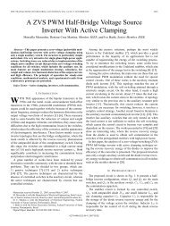
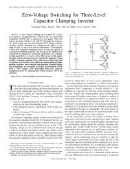
Power Electronics Congress - Ivo Barbi
Power Electronics Congress - Ivo Barbi
Power Electronics Congress - Ivo Barbi

You also want an ePaper? Increase the reach of your titles
YUMPU automatically turns print PDFs into web optimized ePapers that Google loves.
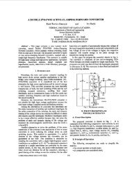
A Different Approach to BUM an Uninterruptible <strong>Power</strong> Snppty Systemwith <strong>Power</strong> Factor Correction.N. Vbzquez* C. AguilaP* J. Alvarez*** R. Cbc~es**** I. <strong>Barbi</strong>**** J. Arau*** fnstituto Tecnol6giro de **CENIDETCelaya<strong>Electronics</strong> EngineeringComputer Sciem Dpt.Celaya, McxiooDPt.Guemavaca MexicoPhone: 521 (73 1) 175-75 Phone: 52 (73 1) 87741Fax: 52 (73 1) 179-79 Fax: 52 (73 1) 224-34E-Mail: nvazque@tc,mx E-Mail: j.amu@itee.org+*** Federal University ofSanta casarina**+CINVESTAV-PN.Electrid Engineering Dpt.Mexico, D.F.Phone: 52 (5) 747-7000Fax: 52 (5) 747-7089&Mail: Fax: 5548-234.5422jalvarez@arI.cinvestav.mx &Mail: hro@incp.ufscbr<strong>Power</strong> <strong>Electronics</strong> InstituteMandpolis -Se- BrazilPfione: 55-48-23 1-9204Besides, the power in- stage is donebased on the full bridge buck inverter (FB-BI).In tbis case the output voltage is always lowerthan the DC input voltage, therefire it isnecessary to add an extra stage to adequaw itsinput voltage. There are two alternatives toachieve this objectiveI. INTRODUC~IONTo add an external UPS is the traditionalapproach used to provide "uptible powerfor applications such as personal computers,medical equipment, telecommunicationsystems, control systems, etc. On the otherhand, it is desirable to inelude power fhctorcorrection (PFC) because of the well knownadvantages that this improvement repraamts.However, in order to get this capacity, it isnecessary to add an extra power stage as it c8nbe observed in Fig, I.The first possibility is to build the inverterstas throughwt the FB-BI and the bOOSthgfunction by using a heavy and bm lowfresuemcy transformer (Fig 2a). The secondpossibility is to use a DC-W boost converterin order to adequate the inverter input voltage(Fig 2b).INMRIfflI---- -TBATTERY SETOWST CONVERTERiF TRANSFORMERINERTERkW -(.' - -T' I ,BATICRY xiFig 1. Traditional unintaruptlble power suppiy systemwith active PFC-TBATTERY SETFig. 2. Traditional dbfn&ves to implement theinvaterstage,(a) low firesuencv AC lid (b) hi& tiesuenCy Dc link.0-7803-5006-5/98/$10.00@'1998 IEEE.119
MA,N {TACTIVE POWER FAC 3R1 ElTp-t-W LGADEAfTEAYcnAwEa-LcTBATE RY SETBGOST CONVERTERINVERTERFig. 3. Unintertuptible powe supply system with active power factcn correction and high hquency DC link.The last option is more suitable due tobenefits such as reduced sh: and low weight.The UPS using a two sage PFC-batterycharger and a two-stage hi:$ fiequency DClink-inverter is shown in Fig 1 .As it can be observed in Fig. 3, the UPSscheme consists of four jower conversionstages resulting in poor efIi;iency, high costand low reliability. In this paper, a novelscheme of an uninterptible power supplysystem based on two power :6nVersiOn stagesis presented. The proposed mfiguration hashigh efficiency and low c.ost. Besides, itexhibits a close unity power E ictor.- INTEGRATEDvac 'I., BnTSERv WARGEU- TWOLOGYPROPOSED SYSTEMThe proposed UPS basell on two powerconversion stages is shown in Fig. 4 (thisapproach was previouSly presented atPESC'97 by the authors 111) The UPS offersexcellent festures, such as: simple structure,high power hctor, low total harmonicdistortion, fast dynamic respnse at the outputvoltage, high efficiency and low cost. Thesefeatures make it a better solution than theclassical approach.INVERTER2/" "INThe first stage of the proposed UPSconsists of an integrated battery charger whichwas presented in [2]. This topology uses adiscontinuous conduction mode (DCM) flybackconverter in ordg to provide high power fictor,battery charging, and high fiequency isolationbetween both the main input and the battery setto the load. This structure does the functions ofbattery charging and power factor correctionusing just one magnetic structure, reducing thecost and accomplishing high reliability andsimplicity of the converter. However, due to theuse of the DCM flyback converter, it issuitable for low power applications (1 500Watts).The second stage is an integrated invertertopology with both boosting and mvertiugfunction. This topology was previouslyintroduced in [3]. The boost DC - ACconverter, refmed to as boost inverter, has anexcellent property: it naturally generates anoutput AC voltage lower or larger than the DCinput voltage, depending on its duty cycle [3-51. This property is not found in the classicalvoltage source inverter which produces aninstantaneous AC output voltage always lowerthan the input DC voltage. In the nextparagraphs the operation principles of eachstage of the proposed UPS structure will bedeSCribed.III. BATTERY CHARGER-PFC STAGEThe bask C~C& Of the ba- ~harger-PFC isshown in Fig. 5. As it caube seen m this figure,the converter acceQt two input powers: onethrough the AC line and the other thoughthe120. .
U - - - -1- 'qi[6]. In backup operation mode the equivalentcircuit is a well know DC-DC flybackconverter. However, as the battery voltage islow, the peak and average curreat are higherthan these ones in normal and chargingoperation mode. Therefore, we must be carefulduring the selection of the battery voltage bus.Fig 5 Integrated battery chargex ts polo@ as input stageof the proposed 1 IPS.A. Experimental resultsIn order to veri@ the battery charger-PFCstage an experimental prototype was designedand built.-The specifications were thefollowing: output power = 250 Watts, inputvoltage 120 volts, VMT = 48 volts, andoutput voltage = 48 volts. The converter wasimplemented in DCM using a mixed device aspower switch in order to increase theefficiency.The experimental input voltage and currentwaveforms in n d ojeration mode areshown in Fig. 6. As it cau be seen, the voltageand current waveforms are in phase. Therefore,a close to one power factor and low THD areobtained.la normal and charging operation modes,the equivalent circuit of the integrated batterycharger topology is 8 ilyback converteroperating in DCM. Therefoie, it behaves in anatural way as a linear km 3 to the utility lineThe converter was tested in chargingoperation mode too. The experimental inputvoltage and current waveforms during thisoperation mode are shown in Fig. 7. As it canbe seen in this figure, the input currentwaveform has a dead time crossing duringzero. This effect is due to the rebrtively high. . . . + ' . , ,' . II, . . .. . . .. . .. . .Fig. 6. @utvoItage and current * vavehrms in normaloperation mod :Fig. 7. Input voltage and current w aveh in chargingoperationmode.121
attery voltage bus [7], causing a reduction ofthe power factor and highs "HD than those innormal operation mode. H8)wever, a higherV, voltage means a higher efficiency inbackup operation mode.The boost inverter acheves DC - ACconversion as follows: the pa wer stage consistsof two current bi-directional boost converterand the load is connected differentially acrossthem (see Fig. 8). These corwrters produce aDC - biased sinusoidal waveform, so that eachconverter produces an unipplar voltage. Themodulation of each con vat^ is 180 dew=out of phase with respect tc the other, whichmaximizes the voltage excwion over the load(Fig. 9).For the purpose of optimizing the boostinverter dynamics, while ensuring correctopea-ittion in any working wrdition, the slidingmode controfler is one of ihe most suitableapproaches f8,9]. The maim advantage, overthe classical cohtral schemes is its robustnessfbr plant parameter variaticns and inwuiantsteady state respowes in the ideal case.ic+ vo -t;;A. Sliding mode controller.Two controllers are used, one for eachboost converter, as a result of this an easiermodel of the system is obtained since one ofthem is modeled as an ideal source. The designsteps [ 10-121 can be Summanzsd - as follow:i) Propose a sliding surfaceii) Verify the existence of sliding modeiii) VerifL stability into the sliding swface.These points are explained in 1121.There€ore only some definitions are mentioned.The propwed sliding surface is:s = sx - sxr = sexWhere:s = [SIsz], controller parametersX = state variablesX, 5 reference variablesex= [ex,The proposed control law is:U=%+*Where: uoq = equivalent control,UN=-SgilGB. Simulation results.(1)The system has been simuiated with thefollowing parameters: L== 360 pH, C=28pF,R=32,4Q, Vin = 50 Volts, Vo = 180 Vac,e60 Hz. In figure 10 and 11 is shown thecapacitor voltage under resistive load and loadvariation respectively.Fig. 8. Boost inverter with slid ng mode coatrolFig 9. Output voltage fbr each I: C-DC converter.Fig. 10 .Simuletions with resistive load122
Fig. 11. Simulation with load NU iation SI 50.8 y spl.C. Etperitnental results.In order to validate the proposed idea, 81300W prototype of the bast inverter wasimplemented, The followiq parametas wereadopted: L = 360 CrH, C =: 28 pF, Vin = 48 V,Vo = 120 Vac, fo = 60 Hz, js mB( = 30 IsHzThe invezter was testec undy no load,linear, nonlineat artd load va riation conditions.The output voltage under to load conditionwith a THD = 0.7% is show in figure 12.The converter d er resb jve load is shownin figures 13 and 14. The c utput voltage andcurreflt is shown in figure 13 and the capacitorvoltage is shown in figure 4 4Fig. 14. C+tavoltage, Pe200W.In order to show the system mp&, it wastested under non linear load and load variation.The output voltage and cunent under aonljneafload that demands 133 VA (C=220pF,R=240S2) is shown in figure 15. The THDobtained in this case is 3.61%.In figure 16 is shown the output voltagetMd cuttent under load variation, the settlingtime when the load decreases and afterincreases is 760pS and 98OpS respectively.In figures 17 and 18 are shown theefficiency and the THD versus the outputpower.Fig. 15 Output vd@p and"liner loadFig. 13. Output voltage and CUI rent, P62OoW... .... ..'.,...,I. I I...,..Fig. 16. Output voltage and mat, load variation.123
’60 100 1M 200 250 300out pat pow^Fig. 17 EfIiciency vs. ou put power.THD%0402‘.ik0 0 50 100 1% :XI _t_i w) MOoutputpmFig 18 THD vs. ouw 1 power.v. CONCLUS14 INSNowadays, it is very imilortant to achievehigh efficiency, low cost and high reliability inUPS design, and at the same time to fblfill thepower quality standard (coicerning PF atndTHD characteristics). This paper presents anovel approach in order to meet theseobjectives which is based or the reduction ofthe power conversion stages in both the batterycharger and the inverter stage 1.A boost inverter torology used inapplications such as UPS is analyzed. Thisconverter is different fi-0~1 the traditionalinverter because it is able to lwst and invert asignal at the same time. This :onverter requiresa k t response, robustnes and stabilityproperties in order to reduce the distortion ofthe output voltage.In order to show the peiformance of thedesigned controller, some simulations andexperhmts have been mde. It can beobserved a good dynarmc resoonse, robustnessand stability properties when the control basedon sliding mode has been appl id.II!IREFERENCES[I] R Ctkeres, N. VgzqueZ C. Aguilar, J. Alvarez, L<strong>Barbi</strong> and J. Arau, “A High Performance of anUnintermptible <strong>Power</strong> Supply System with <strong>Power</strong>Factor Correction”. IEEE <strong>Power</strong> <strong>Electronics</strong>S’ialists CoMerence PESC’97, Vol. 1, pp 304-309.[2] C. Aguilar, F. Canales, J. Arab J. Sebastih and J.Uoeda, “An Integrated Battery ChargedDiwhgerwith <strong>Power</strong> Factor correction”, IEEE <strong>Power</strong><strong>Electronics</strong> Specialist Confwence PESC ’95, pp. 714-719.[3] R CBceres and <strong>Ivo</strong> <strong>Barbi</strong>, ”A Boost DC - ACGmverter: Operation, Analysis, Control andExperimentation”, Proceedings of internationalConference on Industrial <strong>Electronics</strong>, Control andInstrumentation -IECON’95, pp. 946 - 5S1.141 R CBCeres and <strong>Ivo</strong> <strong>Barbi</strong>, ”A Boast DC - ACConverter: Principle of operation, Simulation andImplementation” (in Portuguese), Proceedings of thePmer Electronic Brazilian <strong>Congress</strong> -COBEP’95,pp. 86 - 91.[SI R Wes and <strong>Ivo</strong> <strong>Barbi</strong>, ‘‘Sliding Mode Controllerkr The Boost Inverter”. Proceedings of the IEEEInternational <strong>Power</strong> <strong>Electronics</strong> <strong>Congress</strong> -CIEP-96, p ~. 247 - 252.[6] R Erickson, M. Madigan and S. Singex, “Design ofa Simple High-<strong>Power</strong>-Factw Rectifier Based on theFlyback Converter“, IEEE Applied <strong>Power</strong><strong>Electronics</strong> Confireme -APEC’!M, pp. 792 - 801.[A C. Aguilar, “Analysis of a Novel scheme of anIntegrated Battery Charger/Discharger with High<strong>Power</strong> Factor“ (in Spanish), Ms. Sc. thesis, CeatroNaGional de InvestigsOi6n y Desanrollo T~oI6gico(CENDET), Cuemavaca, MexiCO, February 1995.[8] P. Mattavelli, L Rossetto, G. Spiani, “GeneralPurpose Sliding Mode Controller for &/&Converter Applications”, IEEE <strong>Power</strong> <strong>Electronics</strong>Specialist Coi&rence -PESC’93. pp. 609 - 615.[9] M. Carpita, U Marchesoni, ‘cExperimental Study ofa <strong>Power</strong> Conditioning Using Sliding Mode Control”,IEEE Transactions cm power Electranics, vol. 11NO. 5, Sept. 1996, p ~ 731 . - 742.[IOJR A. Decarlo, S. Zak, G. P. Matthews, “VariableStructure Control of Nonlinear MultivariableSystems: A Tutorial”, Procedings of the IEEE, vol.76 NO. 3, M d 1988. pp. 212 - 232.[ll]V. L Utkin, ‘‘Sliding Modes and Their Applicationin Variable St” System”, MZR Publfdws,Moscow, 1974.[12JN. Vbziquez “New struchue of Inveater Based on thecdd Boost Converter” (in spenish), Ms. SeThesis, Centro Nacional de hvestigacihn yDesarrollo Tecnol6gko (CENIDET), Cwnavaca,Mt%cq November 1997.124