PUTTING CUSTOMERS FIRST - UMC
PUTTING CUSTOMERS FIRST - UMC
PUTTING CUSTOMERS FIRST - UMC

You also want an ePaper? Increase the reach of your titles
YUMPU automatically turns print PDFs into web optimized ePapers that Google loves.
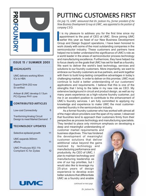
ISSUE 15 / SUMMER 2003highlights<strong>UMC</strong> delivers working 90nmICs to HBA 3SuperH SH4-202 nowSi-verified 4Artisan & <strong>UMC</strong> develop 0.13umPCI Epress PHY core 5contributed articlesLow-cost Connectivity 6Tranforming Analog CircuitDesign to meet Market Demand 7technology updatesSelective epitaxial growth 11<strong>UMC</strong> expands 300mmefforts 11<strong>UMC</strong> Produces 802.11bCompliant IC for Zydas 12<strong>PUTTING</strong> <strong>CUSTOMERS</strong> <strong>FIRST</strong>On July 15, <strong>UMC</strong> announced that Dr. Jackson Hu, former president of theNew Business Development Group at <strong>UMC</strong>, was appointed to the position ofcompany CEO.Iearlier this year as head of our New Business Developmentt is my pleasure to address you for the first time since myappointment to the post of CEO at <strong>UMC</strong>. Since joining <strong>UMC</strong>Group and Design Support operations, I have been honored towork closely with some of the most outstanding companies in thesemiconductor industry. These customers and partners havehelped me to better understand the significance of <strong>UMC</strong>’s role asa world leader in the areas of semiconductor process technologyand manufacturing excellence. Furthermore, they have helped meto focus clearly on the goals that <strong>UMC</strong> has set for itself as a foundry.We want to deliver the world’s best technology, services andsolutions to our foundry customers. More importantly, we want toembrace our foundry customers as true partners, and work togetherwith them to build long-lasting competitive advantages in today’schallenging markets. In order to deliver on this promise, <strong>UMC</strong> mustcontinue to build a better understanding of our customers’applications and requirements. I believe that this is one of thestrengths that I bring to the table in my new role as CEO. Myextensive background in circuit and product design, as well as mymany years experience as a high-volume foundry customer, putme in an excellent position to contribute to the enhancement of<strong>UMC</strong>’s foundry services. I am fully committed to applying myknowledge and experience to make <strong>UMC</strong> the most customerorientedfoundry in the semiconductor industry.As a former foundry customer who has worked with almost allof the major silicon providers over the span of my career, I observedthat foundries tend to approach their customers firmly from theirperspective as process technology and manufacturing specialists.They tended to place only minimum emphasis on developing adeep and meaningful understanding ofcustomer market requirements andbusiness objectives. This has hinderedthe development of meaningfulcustomer solutions that deliveradditional value beyond the gainsrealized by technology andmanufacturing performance andproductivity. As CEO of <strong>UMC</strong>, Iplan to maintain technology andmanufacturing leadership asone of our top priorities, but Iwould also like to leverage my25-plus years of designexperience to develop evenbetter solutions that differentiate<strong>UMC</strong> as a foundry and enablecontinued on next pageDr. Jackson HuPROFOUNDRY SPRING 2003
Partnering For Success, continued from page 1our customers to dominate theirmarkets.As the industry moves toeven deeper sub-micron processtechnologies, elevatedcomplexities have made itincreasingly important that wedevelop total product solutionsfor our customers. This processstarts with design, IP, and EDAsupport and extends throughmanufacturing, back-endassembly and test management,and all the way to end of productlife. Of course, in order to delivertruly valuable solutions, we willhave to build up even strongerinternal capabilities to addressthese issues effectively. I amhappy to report that we havealready made significantprogress in turning our effortsinto real-life results for ourcustomers, and I am confidentthat we will continue to progressat a rapid rate in the days tocome.I would like to share withyou some of the recentmilestones that characterize thetype of results we expect to seefrom our close partnerships withour customers. In March, <strong>UMC</strong>announced the pure-playfoundry industry’s first delivery ofworking products built using 90-nanometer copper/low-ktechnology to Xilinx. We fullyexpect this achievement to furtherconsolidate Xilinx’s leadership inthe highly competitive FPGAmarket. Soon after, one of ouremerging fabless customers,HBA, achieved silicon successat 90nm for their newest productprototype. Only throughextremely close partnerships canfoundry customers expect to seethese types of early results.Going forward, <strong>UMC</strong> willcontinue to extend its leadershipin 300mm wafer manufacturingand 90nm and beyondtechnologies. We stronglybelieve that 300mmmanufacturing will play anincreasing role in our customers’success, especially for complexsystem chips. As process linewidthsshrink to 90nm and belowand die size increases due tomore sophisticated SoC designs,the potential for productivitygains increases greatly. WithFab12A in volume production for0.13um customer products and<strong>UMC</strong>i entering pilot production,<strong>UMC</strong>’s 300mm leadership with90nm and below designs will bea key tool to help our partnersrealize further competitiveadvantages.Finally, I hope that <strong>UMC</strong>’sstrengthened focus on customerorientedsolutions will greatlyenhance the competitiveness ofour customers, and I amconfident that together we canreap the benefits of strong andcompelling partnerships.Dr. Jackson Hu -Fact File-25-year semiconductor industryveteran-Former President and CEO ofSiRF Technology-Founded both IC Ensemble andVerticom-Former senior vice president andgeneral manager of S3-Earned BA in electricalengineering from National TaiwanUniversity-Earned Masters and PhD incomputer science from theUniversity of Illinois, Urbana, andan MBA from Santa ClaraUniversity.<strong>UMC</strong>’s operating priorities1. <strong>UMC</strong> will accelerate its 300mm investment to expand capacity at Taiwan’s Fab 12A to20,000 wafers per month, and capacity at <strong>UMC</strong>i to 10,000 wafers per month by the endof 2004.2. <strong>UMC</strong> will further strengthen its R & D efforts for 90nm and below process technologies,and ensure the availability of a complete catalog of relevant IP for integration in itscustomers’ leading-edge designs.2PROFOUNDRY SPRING 2003
IP FocusSuperH SH4-202 CPU Core AchievesSilver IP Status at <strong>UMC</strong>SuperH’s SH4-202 32-bit CPU core hasachieved “Silver IP” status at <strong>UMC</strong> for thefoundry’s 0.13um process, signifying that thecore has been verified in silicon under <strong>UMC</strong>’s GoldIP program and is ready for production.The SH-4 family is targeted at a wide range ofmultimedia applications including set top box, carinformation systems and portable digital consumerproducts and is supported through SuperH’sextensive 3 rd party program with over 65 companiesoffering various development tools, software anddesign services.The “Silver IP” status of the SH4-202 willbecome “Gold IP” once a customer design that usesthe core achieves volume production at <strong>UMC</strong>. TheGold IP program makes available to customers awide range of silicon verified IP and librarycomponents that are optimized for easy integrationinto customer designs.The SH4-202 CPU core integrates a 32-bit RISCCPU core with an integrated Vector floating pointunit and delivers an impressive 1.5 Dhrystone 2.1MIPS/MHz and 7MFLOPS/MHz. In 0.13um CMOS the CPUcore is less than 1mm 2 and thewhole hard macro integratingCPU, FPU, 32K D cache, 16K Icache, serial port, timers, realtime clock, interrupt controller,bus interface and debug port is only 8.2mm 2 .PerformanceDhrystone 2.1:Floating point operations:Complex FFT 1024 point radix 2:16-tap, 40-sample Block FIR:EEMBC:BDTIMark2000:3D polygons:ITU-T G.729 Annex C (8k/s):VoIP channels (full G.729):1.5 DMIPS / MHz7 MFLOPS / MHz4 cycles / complex butterfly1.6 MACs / cycleSee http://www.eembc.org750 at 240MHz9.3M/s at 266MHzRequires 25MHz and40k bytes39MHz CPU performance perchannelAbout <strong>UMC</strong>’s Gold IP ProgramOverview<strong>UMC</strong>’s Gold IP program helps designers andsystem developers overcome system-on-chip(SOC) and time-to-market hurdles by providingeasy access to third party IP blocks ready forintegration into customer designs. In the program,<strong>UMC</strong> has partnered with strategic IP partners toestablish a pool of IP solutions that are driven bymarket segment and customer needs. The IP isclassified as Bronze, Silver, or Gold, depending onthe level of maturity.Rating and Criteria4PROFOUNDRY SPRING 2003
IP FocusArtisan & <strong>UMC</strong> Collaborate on PCIExpress Compliant 0.13um PHY CoreThe collaborative effortsbetween Artisan Componentsand <strong>UMC</strong> for IPand design resources haveshifted towards the developmentof a PCI Express TM PHY IP corefor 0.13-micron chip designs.The new core will be based onthe PCI Express Architecturethat has been proposed by thePCI-SIG® (PCI Special InterestGroup), which owns andmanages PCI specifications asopen industry standards.Based on Artisan’s siliconprovenXAUI compatible SerDesCore, the PHYs modulararchitecture enables a broadrange of computing andcommunications targetapplications emphasizingperformance, cost andscalability. The open architectureof the PCI Express to which thisoffering will comply will helpdesigners more easily integratethe core into their 0.13umproduct designs, and will offerthe benefits of high performanceand design flexibility.The PCI-Express TM 2.5GbpsPHY targets <strong>UMC</strong>’s 0.13-micronprocess technology. Themodular 8-lane PCI Express TM2.5Gbps PHY is designed to bea general-purpose I/Ointerconnect for “in-the-box”applications. Its architectureprovides a connectivity solutionfor adapter cards, attach pointsfor graphics I/Os as well as anI/O attach point for otherinterconnects like 1394b, USB2.0, Infiniband and Ethernet. ThePCI Express PHY creates acomplete serial link includingmux/demux, 8b/10b encode/decode and clock recoverycircuitry which is compliant withthe PCI Express Specification.The core is slated for availabilityto customers in the fourth quarterof 2003.About PCI ExpressPCI Express architectureis a state-of-the-art serialinterconnect technology thatkeeps pace with recent advancesin processor and memorysubsystems. From its initialrelease at 0.8V, 2.5GHz, the PCIExpress technology roadmap willcontinue to evolve, whilemaintaining backward compatibility,well into thenext decade with enhancementsto itsprotocol, signaling,electromechanical andother specifications.The PCI Expressarchitecture retains thePCI usage model andsoftware interfaces forinvestment protection andsmooth development migration.The technology is aimedat multiple market segments inthe computing and communicationindustries, andsupports chip-to-chip, board-toboardand adapter solutions atan equivalent or lower coststructure than existing PCIdesigns. PCI Express currentlyruns at 2.5Gbps, or 250MBpsper lane in each direction,providing a total bandwidth of16GBps in a 32-laneconfiguration. Future frequencyincreases will scale up totalbandwidth to the limits of copperand significantly beyond that viaother media without impactingany layers above the PhysicalLayer in the protocol stack. PCIExpress provides I/O attachpoints for high-performancegraphics, 1394b, USB 2.0,InfiniBand Architecture,Gigabit networking and so on.PROFOUNDRY SPRING 20035
Customer Product FocusLow-cost ConnectivityContributed by Raymond Xue, Technical Marketing Manager, ZiLOG Inc.Connectivity in the currentcontext refers to a broadrange of technologies thatallow various embedded systemsor subsystems to communicatewith each other or with humanusers over certain geographicareas in order to process eventsand data effectively. Traditionallytechnology, thanks to the wideacceptance of the Internet andthe ability of TCP/IP to run overdifferent types of physicalnetwork interfaces. Although theTCP/IP standard was defined forthe desktop world and typicallyrepresents high implementationcost requiring 16/32-bit micro-solutions suchas ZiLOG’seZ80 Acclaim MCUs aretaking on challengesthatonce belonged to the 16/32-bitdomain.Accomplishing this feat“High-performance 8-bit microcontrollers willfuel much of the growth for embedded connectivitysimply due to lower cost.”such communication takes placeover proprietary protocols andphysical interfaces, usually in theinterest to optimize systemperformance and cost. Thisapproach leads to a wide varietyof incompatible connectivitysolutions in the market today.A proliferation of standardsis now the driving force behindembedded connectivity, bothwired and wireless. In an effortto increase interoperability,reduce risk, and lower cost ofownership, OEM vendors andcustomers alike are embracingstandards driven solutions fortheir products and services.Leading the adoption curve isthe embedded TCP/IPprocessors, embedded TCP/IPtechnology is making its way into8-bit based systems due to theavailability of high-performance8-bit microcontrollers.High-performance 8-bitmicrocontrollers will fuel much ofthe growth for embeddedconnectivity simply due to lowercost.Standardized connectivityensures interoperability, butlower system cost brings massmarket acceptance. For example,in the same way that smallerembedded systems today havereplaced complex PCs in manyapplications due to better featureintegrations and increasedperformance, capable 8-bitfollows the principle that newproducts today must offercustomers better features andperformance while loweringsystem cost. By integratingmemory and networkinghardware into 8-bit devices withcore performance of 50MHz andbeyond, these high-performance8-bit MCUs can provideembedded connectivity whileexecuting traditional applications.Further development ofthese high performance deviceswill ultimately align 8-bit systemthroughput to the current 16/32-bit’s without increasing cost.For more information on Zilog,please visit their website atwww.zilog .com6PROFOUNDRY SPRING 2003
Design Methodology FocusTransforming Analog Circuit Designto Meet Market DemandContributed by Amit Nanda – Director of Solutions Marketing, BarcelonaAs communications and consumer devices—such ascell phones, DVD players, high-speed networks anddigital cameras—swell in popularity, so does thedemand for analog circuitry. These high-growthapplications are drastically altering thesemiconductor market. Whereas ten years ago, PCand computer applications that required digital, andby current standards, low frequency circuits,dominated industry shipments, today consumer andcommunications applications reign. And, all of theseapplications require integration of digital componentsas well as real-world interfaces that only analog canprovide.In fact, over the last five years, the mixed-signalsystem-on-chip market has seen consistentgrowth. Technical advances in integrated circuit(IC) manufacturing processes have made it possiblefor true electronic systems, such as cameras andradio systems, to be integrated on a single siliconsubstrate. Within the next three years, seven outof ten systems-on-chips (SOCs) will contain analog(source: IBS, May 2001). The result will be afundamental shift in IC design processes over thenext several years. And, because of the extensivedesign time required for analog content in mixedsignalSOCs, the industry is facing a seriousshortage in analog supply. A bottleneck in analogcircuitry is the unfortunate result, one that imperilsthe growing semiconductor industry. Overcomingthis bottleneck requires nothing short of radicallynew technology that breaks free of thirty years ofanalog design stagnation.Barcelona Design discovered that geometricprogramming—a type of nonlinear optimizationproblem—holds the key. By applying geometricprogramming to circuit design, Barcelona providessemiconductor companies with a means to designanalog blocks in hours rather than months. In short,enabling them to circumvent the bottleneck. <strong>UMC</strong>and Barcelona have forged an alliance to ensurethat their common customers have access to thisrevolutionary technology. This article explores theroots of the analog shortage, discusses the currentoptions for designing analog blocks and explicateshow Barcelona’s technology addresses theproblem, and highlights the benefits to <strong>UMC</strong>customers and other semiconductor companies.Analog BottleneckWhile growing demand is always beneficial tothe industry, it can also prove challenging whensupply remains essentially flat. In the case of analogcircuit supply, the problem stems from severalfactors. First, in the last twenty years, the industryhas focused largely on digital, leaving a dearth ofengineers who understand analog circuit design.Today, analog circuit designers are scarce;estimates place the number of analog designers atfewer than 10,000 worldwide. Most chip designersspecialize in the highly automated digital designprocess and have little knowledge or training inthe manual art of analog design.Second, analog design is as much an art as ascience. To acquire expertise in analog design,engineers typically apprentice for several years withan analog expert, or spend a greater number ofyears being self-taught before they are able todevelop good designs.Finally, designing analog circuits is, on thewhole, a manual process that has seen littlefundamental improvement in thirty years. It is stilldependent on SPICE circuit simulation and a trialand-errorprocess that can take months. While theindustry has made efforts to speed up this process,no progress has been made that compares to thecontinued on next pagePROFOUNDRY SPRING 2003 7
continued from page 7specification-driven, synthesisbaseddesign common in digitalcircuits.Compounding the problem,design times for analog circuitshave also shrunk. Becauseanalog and digital circuitry nowco-exist on a single chip, allcircuits must be ready for chipfinishing at the same time. Thus,in a growing industry, we face thechallenge of getting a limitednumber of analog designers (whocurrently use age-old manualmethods) to design analogcircuits at faster rates to meetdemand.Furthermore, the rapidlychanging applications for SOCsrequire a greater breadth ofavailable analog circuits; circuitsthat are customized to meet exactproduct specifications, robustenough to work in the full chipprototype and productionphases, and flexible enough toallow modification ofspecifications through the designprocess.Why not address theserequirements by designingcustom circuits or using preexistingblocks? Because bothapproaches fall far short ofsolving the analog bottleneckand providing high-performance,flexible circuits. While developingcustom circuits may enable somecompanies to get highperformanceblocks that closelymeet requirements, the processfor creating custom analogblocks is inflexible, not scalable,and extremely slow.Short of designing your owncustom analog block (orpurchasing it from anothercompany that custom designs itfor you), the other option forobtaining analog circuits is to usepre-existing blocks that havebeen designed for a targetprocess technology. Theseblocks are pre-designed circuitsthat may have been designed foranother purpose and offered forsale, or they may be so-called“library” circuits intended for usein many SOC designs.However, a pre-designedcircuit is fundamentally limited: itrarely meets requiredspecifications exactly and cannotbe altered without an expensive,time-consuming consultingproject. The bottom line is that apre-designed circuit is dead onarrival since it has limited reuseand no shelf life.Traditional custom circuitsand pre-design blocks are bothriddled with problems andultimately fail to addressincreasing industry demands—the bottleneck remains.Geometric Programming:Solution to the AnalogBottleneckThis shortage ofcustomized, scalable analogcircuitry is no small challenge tothis industry and to <strong>UMC</strong>customers. And, it’s the veryproblem that Barcelona Designhas resolved by developing anew alternative for creating andmodifying analog intellectualproperty: analog synthesis basedon geometric programming. Thismethod enables companies tobuild robust, customized analogblocks incredibly quickly.For the first time in thirtyyears, the process for designinganalog circuits has dramaticallychanged. Using this analogsynthesis solution, designers nolonger need to rely on traditional,simulation-based designmethods. The result is a moreoptimal tradeoff amongperformance and cost variables.Most importantly, the new,custom analog circuit can becreated, down to tapeout-readyGDSII, in a matter of hours. Thisremarkable synthesis speedallows the designer to quicklyexperiment with the blockperformance and cost to get asense for the possibilities,eliminating time often spent oninfeasible and impractical designpoints.For example, a designermay need a PLL with the lowestpossible jitter. But, he also haspower constraints. He will beable to evaluate the possibilitiesand tradeoffs between differentdesign points so that he canidentify what is technicallypossible and the optimal point foreach design element. As shownin Figure 3, Barcelona’s solutionilluminates the tradeoff curvebetween power and accumulatedjitter.In this way, the designer canquickly explore the design spacebefore committing to anyspecifications. After determiningwhat is possible, he then selectsthe preferred design point andcreates the files necessary forintegration, including abehavioral model and GDSII file.How does BarcelonaDesign change a process thathas—for decades—takenmonths, into a process that takesjust hours? It’s all aboutmathematics. Barcelona’s8PROFOUNDRY SPRING 2003
“By bringing Barcelona’s uniquecapabilities to <strong>UMC</strong>, we will now beable to provide the analog IP flexibilitydesired by our customers withoutcompromising time-to-market orperformance.” Dr. Jackson Hu, CEOof <strong>UMC</strong>.Figure 3: Optimal trade-off curve between accumulated jitterand minimum powersolutions solve a whole set of equations thatexpress performance characteristics as a functionof physical characteristics, such as transistor sizing,placement and interconnect. The equations arevery detailed, taking into account a series ofcomplex variables, including process, voltage andtemperature variation; noise conditions; circuitbehavior and process characteristics. The key tothe whole process: Barcelona’s solution takes allof these different characteristics into accountsimultaneously in order to create an optimal andextremely robust circuit.Using geometric programming (GP),Barcelona combines process information with circuittopology to develop very accurate proprietarymodels. A geometric program is a special type ofnonlinear optimization problem that not onlycaptures design constraints and relates designvariables to the specifications, but also can betransformed into a convex problem. Convexityenables the rapid and certain determination of aglobal solution to the optimization problem, essentialto use in analog design.Geometric programming has been known andused since the late 1960s, and has more recentlybeen used in transistor and wire sizing for Elmoredelay minimization in digital circuits, as incommercial tools such as TILOS. The emergenceof Barcelona’s technology, however, marks the firsttime that geometric programming has beensuccessfully applied to analog circuit design.Barcelona has proven its technology in thefabrication of five leading semiconductormanufacturers through extensive silicon-basedcharacterization. As part of this effort, Barcelonahas taped out and achieved 100 percent first siliconsuccess on PLLs and data converters in fourprocess technology generations from 0.25 um downto 90 nm.There are three steps to Barcelona’s newmethod for creating analog circuits. First, circuitmodeling. After selecting a final circuit architecture,the circuit’s electrical and physical behavior isexpressed in a special mathematical form(geometric programming) with three key properties:Process independence—Once a cell isdescribed in this form it is available for any process.For example, the gain of a differential pair in anamplifier is expressed as gm*RL. This expressionfor gain is the same in any process. The descriptionrepresents the behavior of the circuit and remainsprocess independent.Hierarchy—The models are written in a modularand hierarchical way. This allows the reuse ofblocks (i.e. the same op-amp can be used in a PLLor ADC), easy updates and efficient new enginecreation.Accuracy—GP allows for very detailed andcontinued on next pagePROFOUNDRY SPRING 2003 9
continued from page 9accurate representations ofhighly complex electrical andphysical behavior.Second, process modeling.In parallel with circuit modeling,the target process is modeled inGP form. Electrical and physicalprocess information fortransistors, capacitors, resistors,inductors and any other processdependentcomponent is alsomodeled in geometricprogramming form. Key toBarcelona’s approach is the factthat the models include bothelectrical and physical behavior.For example, at the time ofsynthesis, Barcelona has a veryaccurate expression of aMOSFET’s drain-to-bulkcapacitance since it not onlydepends on electricalparameters, but also on how thespecific cell is laid out.Third,GP-based optimization.With the circuit andprocess models completed,customers may use Barcelonasynthesis solutions to generatecircuits based on their ownunique specifications. Customerspecifications serve asoptimization objectives and/orconstraints within a geometricprogram problem (GP). Thegeometric program is thenglobally solved and its solutionis a physical design that meetsthe user target specifications.These GPs can be solved veryquickly even for very largecircuits. In every case,Barcelona’s technology presentseither a global minimum ormathematical proof that theproblem is infeasible. Thistechnique sharply contrasts tothe traditional simulation-basedmethods that can get stuck in alocal minimum or, if they cannotfind a solution, are unable toguarantee whether a solutiondoes or does not exist. Once theoptimization problem is solved,customers will have a tapeoutreadycircuit that can be directlyplaced in an SOC.Through the <strong>UMC</strong>-Barcelona alliance, <strong>UMC</strong>customers will now have accessto customized circuits that meettheir exact specifications withinhours or days rather than weeksor months; robust circuitsguaranteed to work in a realproduction SOC environment;and flexibility that allow designersto rapidly obtain desiredspecifications at any step of theprocess, from concept totapeout.<strong>UMC</strong> and Barcelona willwork together to understand theircustomers’ current and futureanalog requirements. They willanalyze analog needs fordifferent end user applications inconjunction with the variousprocess options to providesolutions that best suit eachapplication. As a result, thecompanies will offer synthesizableanalog circuits andproduct roadmaps that arespecialized to meet all customerrequirements. <strong>UMC</strong> andBarcelona will also cooperateduring the early stage of aprocess technology. BecauseBarcelona’s technology enablesprocess-independent circuits, itenables rapid support for adeveloping and maturing processtechnology. Thus, Barcelona willprovide <strong>UMC</strong> with feedback onprocess performance whilesimultaneously creating synthesizableanalog circuits that areupdated to meet the most currentprocess design kit.Barcelona will also provide<strong>UMC</strong> with product and trainingnecessary to generate optimizedanalog blocks for theircustomers. And, whether acustomer needs access to thesynthesis solutions or customizedinstances, <strong>UMC</strong> andBarcelona will establish deliverymodels best aligned to thecustomers’ needs.In short, a field that has seenlittle change in thirty years hasbeen transformed by Barcelona’snew technology. For <strong>UMC</strong>customers, this translates intohigh-performance, flexibleanalog circuits, ready when theyare.Barcelona can be found on the webat www.barcelonadesign.com10PROFOUNDRY SPRING 2003
<strong>UMC</strong> Researching Selective EpitaxialGrowth for Sub-65nm Technology<strong>UMC</strong> is making progress in its research inselective epitaxial growth, or SEG, as acomplementary approach to tacklingproblems of transistor leakage at the sub-65nmnode. Selective epitaxial growth may offerdesigners of high-performance devices a moreconventional solution if integration problems canbe overcome, both for traditional 2-D devices andthe new 3-D devices currently being explored inthe industry.<strong>UMC</strong> is investigating the benefits of theselective application of an epitaxial layer, includingreduced source/drain junction leakage, reducedcontact resistance and its use as a buffer layer forshallow junction implant and as a sacrificial layerfor selective silicide processing. The method isattractive because its selectivity limits its growth tothe silicon surface, not oxide or other non-siliconsurfaces. Selective epitaxial growth would likelyadd a few steps to the process flow, but wouldn’trequire extra masking layers. Just as important,SEG has been used in the formation ofheterojunction bipolar transistors, giving it somehistory and familiarity within the industry.Yet there are also many unknowns related tointegrating SEG into a bulk CMOS process. Oneof the key integration hurdles is overcoming thehigh thermal budget needed for growing the epitaxiallayer. During growth, the temperature exceeds800°Celsius, which damages dopants beneath thegate and skews the device characteristics. Thoughepitaxial layers have been grown under lowtemperatureconditions, the trade off is very lowwafer throughput. <strong>UMC</strong> researchers will continuetheir work to find breakthroughs for this promisingtechnology.<strong>UMC</strong> Expands 300mm Efforts toIncrease 300mm LeadMC has increased its investment in its300mm manufacturing facilities in bothTaiwan and Singapore, further increasing U<strong>UMC</strong>’s leadership position for advanced 300mmmanufacturing. By the end of 2004, <strong>UMC</strong> expectsto expand capacity at Taiwan’s Fab 12A to 20,000wafers per month (50,000 200mm equivalents), andcapacity at its <strong>UMC</strong>i Singaporeaffiliate to 10,000 wafers permonth. Fab 12A has already beenin volume production forcustomer products since early2002 and <strong>UMC</strong>i is continuing onpace with equipment move-in.This 300mm reaffirmation alsocoincides with <strong>UMC</strong>’s recentTaiwan Fab 12Aannouncement that the company will furtherstrengthen research and development for 90nm andbelow process technologies. The combination of90-nanometer and 300mm manufacturing createstremendous productivity advantages, up to as manyas 5 times the number of die per wafer whencompared to 0.13um on 8-inch wafers.Singapore <strong>UMC</strong>iPROFOUNDRY SPRING 2003 11
New CustomersFor new customer inquiries,please direct all questions tosales@umc.comHeadquarters:<strong>UMC</strong>No. 3, Li-Hsin 2nd Road,Science-Based Industrial Park,Hsinchu City, Taiwan, R.O.C.Tel: 886-3-578-2258Fax: 886-3-577-9392Email: foundry@umc.comIn USA:<strong>UMC</strong> USA488 De Guigne Drive,Sunnyvale, CA 94085, USATel: 1-408-523-7800Fax: 1-408-523-8166Email: sales@umc-usa.comIn Europe:<strong>UMC</strong> Europe BVHogehilweg 19,1101 CB Amsterdam,The NetherlandsTel: 31-20-697-0766Fax: 31-20-697-7826Email: europe@umc.comIn Japan:<strong>UMC</strong> Japan7F, Niikura Bldg.,2-2, Kandatsukasa-Cho,Chiyoda-Ku, Tokyo,101-0048, JapanTel : 81-3-5294-2701Fax: 81-3-5294-2707Email: foundry@umcj.comProFoundry is a publication of<strong>UMC</strong>. Please submit commentsand story ideas toprofoundry@umc.com.ProFoundry may be foundonline at the literature sectionof <strong>UMC</strong>’s website:www.umc.comPROFOUNDRYSUMMER 2003ISSUE 15PROFOUNDRY SPRING 2003<strong>UMC</strong> Produces 802.11b CompliantICs for Zydas on 0.18um MixedsignalTechnology<strong>UMC</strong> is currently manufacturing ZyDAS’ newly releasedZD1202, an 802.11b fully compliant single-chip mediumaccess controller (MAC) and baseband processor (BBP) using<strong>UMC</strong>’s 0.18-micron mixed-signal process technology. The chip isdesigned to meet users’ high throughput, low-power and high-securityrequirements.<strong>UMC</strong>’s 0.18um mixed-signal technology coupled with ZyDAS’sunique multipath decoding technology enables the ZD1202 to realizethe full advantage of 802.11b’s complimentary code keying (CCK)even in the presence of severe multipath distortion. As a result, theZD1202 can enlarge the coverage area of 802.11b and work inenvironments where other 802.11b products would fail.Norman Hung, President of ZyDAS Technology, stated, “Thefabrication of this technology would not be possible without theassistance of a truly supportive semiconductor foundry. <strong>UMC</strong> hasplayed an instrumental role in our success as it delivers leadingprocess technology with the design support services to ensure highyields and first-silicon success.”<strong>UMC</strong> has cooperated with ZyDAS for nearly two years for theproduction of their wireless communication IC solutions. The ZD1202is currently ramping to volume production.