ADV7128 CMOS 80 MHz, 10-Bit Video DAC - Analog Devices
ADV7128 CMOS 80 MHz, 10-Bit Video DAC - Analog Devices
ADV7128 CMOS 80 MHz, 10-Bit Video DAC - Analog Devices

Create successful ePaper yourself
Turn your PDF publications into a flip-book with our unique Google optimized e-Paper software.
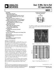
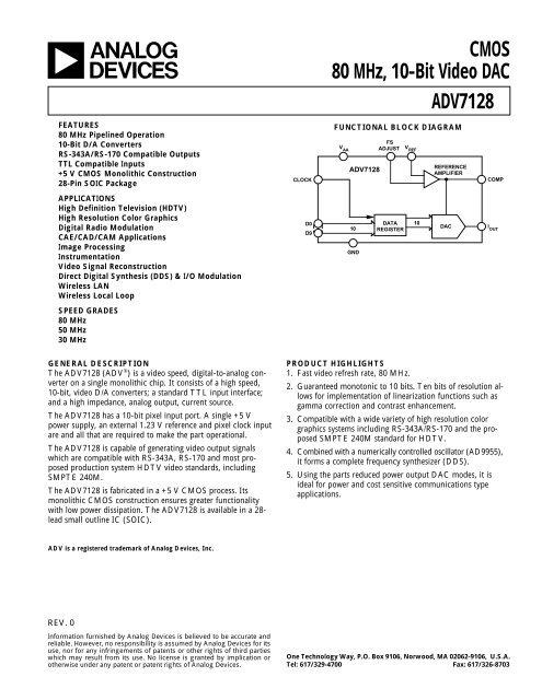
a<strong>CMOS</strong><strong>80</strong> <strong>MHz</strong>, <strong>10</strong>-<strong>Bit</strong> <strong>Video</strong> <strong>DAC</strong><strong>ADV7128</strong>FEATURES<strong>80</strong> <strong>MHz</strong> Pipelined Operation<strong>10</strong>-<strong>Bit</strong> D/A ConvertersRS-343A/RS-170 Compatible OutputsTTL Compatible Inputs+5 V <strong>CMOS</strong> Monolithic Construction28-Pin SOIC PackageCLOCKFUNCTIONAL BLOCK DIAGRAMV AA<strong>ADV7128</strong>FSADJUSTV REFREFERENCEAMPLIFIERCOMPAPPLICATIONSHigh Definition Television (HDTV)High Resolution Color GraphicsDigital Radio ModulationCAE/CAD/CAM ApplicationsImage ProcessingInstrumentation<strong>Video</strong> Signal ReconstructionDirect Digital Synthesis (DDS) & I/O ModulationWireless LANWireless Local LoopD0D9<strong>10</strong>GNDDATAREGISTER<strong>10</strong><strong>DAC</strong>I OUTSPEED GRADES<strong>80</strong> <strong>MHz</strong>50 <strong>MHz</strong>30 <strong>MHz</strong>GENERAL DESCRIPTIONThe <strong>ADV7128</strong> (ADV ® ) is a video speed, digital-to-analog converteron a single monolithic chip. It consists of a high speed,<strong>10</strong>-bit, video D/A converters; a standard TTL input interface;and a high impedance, analog output, current source.The <strong>ADV7128</strong> has a <strong>10</strong>-bit pixel input port. A single +5 Vpower supply, an external 1.23 V reference and pixel clock inputare and all that are required to make the part operational.The <strong>ADV7128</strong> is capable of generating video output signalswhich are compatible with RS-343A, RS-170 and most proposedproduction system HDTV video standards, includingSMPTE 240M.The <strong>ADV7128</strong> is fabricated in a +5 V <strong>CMOS</strong> process. Itsmonolithic <strong>CMOS</strong> construction ensures greater functionalitywith low power dissipation. The <strong>ADV7128</strong> is available in a 28-lead small outline IC (SOIC).PRODUCT HIGHLIGHTS1. Fast video refresh rate, <strong>80</strong> <strong>MHz</strong>.2. Guaranteed monotonic to <strong>10</strong> bits. Ten bits of resolution allowsfor implementation of linearization functions such asgamma correction and contrast enhancement.3. Compatible with a wide variety of high resolution colorgraphics systems including RS-343A/RS-170 and the proposedSMPTE 240M standard for HDTV.4. Combined with a numerically controlled oscillator (AD9955),it forms a complete frequency synthesizer (DDS).5. Using the parts reduced power output <strong>DAC</strong> modes, it isideal for power and cost sensitive communications typeapplications.ADV is a registered trademark of <strong>Analog</strong> <strong>Devices</strong>, Inc.REV. 0Information furnished by <strong>Analog</strong> <strong>Devices</strong> is believed to be accurate andreliable. However, no responsibility is assumed by <strong>Analog</strong> <strong>Devices</strong> for itsuse, nor for any infringements of patents or other rights of third partieswhich may result from its use. No license is granted by implication orotherwise under any patent or patent rights of <strong>Analog</strong> <strong>Devices</strong>.One Technology Way, P.O. Box 9<strong>10</strong>6, Norwood, MA 02062-9<strong>10</strong>6, U.S.A.Tel: 617/329-4700 Fax: 617/326-8703
<strong>ADV7128</strong>–SPECIFICATIONS (V AA = +5 V 5%; V REF = +1.235 V; R L = 37.5 , C L = <strong>10</strong> pF; R SET = 560 .1All specifications T MIN to T MAX unless otherwise noted.)Parameter K Version Units Test Conditions/CommentsSTATIC PERFORMANCEResolution <strong>10</strong> <strong>Bit</strong>sAccuracyIntegral Nonlinearity, INL ± 1 LSB maxDifferential Nonlinearity, DNL ± 1 LSB max Guaranteed MonotonicGray Scale Error ± 5 % Gray Scale max Max Gray Scale Current = (V REF * 7,969/R SET ) mACodingBinaryDIGITAL INPUTSInput High Voltage, V INH 2 V minInput Low Voltage, V INL 0.8 V maxInput Current, I IN ± 1 µA max V IN = 0.4 V or 2.4 V2Input Capacitance, C IN <strong>10</strong> pF maxANALOG OUTPUTGray Scale Current Range 15 mA min22 mA maxOutput CurrentWhite Level 16.74 mA min Typically 17.62 mA18.50 mA maxBlack Level 0 µA min Typically 5 µA50 µA maxLSB Size 17.28 µA typOutput Compliance, V OC 0 V min+1.4 V max2Output Impedance, R OUT <strong>10</strong>0 kΩ typ2Output Capacitance, C OUT 30 pF max I OUT = 0 mAVOLTAGE REFERENCEVoltage Reference Range, V REF 1.14/1.26 V min/V max V REF = 1.235 V for Specified PerformanceInput Current, I VREF –5 mA typPOWER REQUIREMENTSV AA 5 V nomI AA 125 mA max Typically <strong>80</strong> mA: <strong>80</strong> <strong>MHz</strong> Parts<strong>10</strong>0 mA max Typically 70 mA: 50 <strong>MHz</strong> & 35 <strong>MHz</strong> PartsPower Supply Rejection Ratio 2 0.5 %/% max Typically 0.12%/%: f = 1 kHz, COMP = 0.1 µFPower Dissipation 625 mW max Typically 400 mW: <strong>80</strong> <strong>MHz</strong> Parts500 mW max Typically 350 mW: 50 <strong>MHz</strong> & 30 <strong>MHz</strong> PartsDYNAMIC PERFORMANCEGlitch Impulse 2, 3 50 pV secs typ<strong>DAC</strong> Noise 2, 3, 4 200 pV secs typNOTES1 Temperature range (T MIN to T MAX ); 0°C to +70°C.2 Sample tested at +25°C to ensure compliance.3 TTL input values are 0 to 3 volts, with input rise/fall times ≤3 ns, measured between the <strong>10</strong>% and 90% points. Timing reference points at 50% for inputs andoutputs. See timing notes in Figure 1.4 This includes effects due to clock and data feedthrough.Specifications subject to change without notice.–2–REV. 0
TIMING CHARACTERISTICS 1 (V AA = +5 V 5%; V REF = +1.235 V; R L = 37.5 , C L = <strong>10</strong> pF; R SET = 560 .All specifications T MIN to T MAX2unless otherwise noted.)<strong>ADV7128</strong>Parameter <strong>80</strong> <strong>MHz</strong> Version 50 <strong>MHz</strong> Version 30 <strong>MHz</strong> Version Units Conditions/Commentsf MAX <strong>80</strong> 50 30 <strong>MHz</strong> max Clock Ratet 1 3 6 8 ns min Data & Control Setup Timet 2 2 2 2 ns min Data & Control Hold Timet 3 12.5 20 33.3 ns min Clock Cycle Timet 4 4 7 9 ns min Clock Pulse Width High Timet 5 4 7 9 ns min Clock Pulse Width Low Timet 6 30 30 30 ns max <strong>Analog</strong> Output Delay20 20 20 ns typt 7 3 3 3 ns max <strong>Analog</strong> Output Rise/Fall Time3t 8 12 15 15 ns typ <strong>Analog</strong> Output Transition TimeNOTES1 TTL input values are 0 to 3 volts, with input rise/fall times ≤3 ns, measured between the <strong>10</strong>% and 90% points. Timing reference points at 50% for inputsand outputs. See timing notes in Figure 1.2 Temperature range (T MIN to T MAX ): 0°C to +70°C3 Sample tested at +25°C to ensure compliance.Specifications subject to change without notice.t 4t 5t 8t 7CLOCKt 3t 1t 2DIGITAL INPUTSD0–D9DATAt 6ANALOG OUTPUTS(I OUT)NOTES1. OUTPUT DELAY ( t 6) MEASURED FROM THE 50% POINT OF THE RISING EDGE OF THE CLOCK TO THE 50%POINT OF FULL-SCALE TRANSITION.2. TRANSITION TIME ( t 8) MEASURED FROM THE 50% POINT OF FULL-SCALE TRANSITION TO WITHIN 2% OF THEFINAL OUTPUT VALUE.3. OUTPUT RISE/FALL TIME ( t 7) MEASURED BETWEEN THE <strong>10</strong>% AND 90% POINTS OF FULL-SCALE TRANSITION.Figure 1. <strong>Video</strong> Input/Output TimingRECOMMENDED OPERATING CONDITIONSParameter Symbol Min Typ Max UnitsPower Supply V AA 4.75 5.00 5.25 VoltsAmbient OperatingTemperature T A 0 +70 °COutput Load R L 37.5 ΩReference Voltage V REF 1.14 1.235 1.26 VoltsORDERING GUIDEAccuracy Temperature PackageModel Speed DNL INL Range Option*<strong>ADV7128</strong>KR<strong>80</strong> <strong>80</strong> <strong>MHz</strong> ±1 ±1 0°C to +70°C R-28<strong>ADV7128</strong>KR50 50 <strong>MHz</strong> ±1 ±1 0°C to +70°C R-28<strong>ADV7128</strong>KR30 30 <strong>MHz</strong> ±1 ±1 0°C to +70°C R-28*R = SOIC.REV. 0 –3–
<strong>ADV7128</strong>ABSOLUTE MAXIMUM RATINGS *V AA to GND . . . . . . . . . . . . . . . . . . . . . . . . . . . . . . . . . . .+7 VVoltage on Any Digital Pin . . . . . . GND –0.5 V to V AA +0.5 VAmbient Operating Temperature (T A ) . . . . . . . . 0°C to +70°CStorage Temperature (T S ) . . . . . . . . . . . . . . . –65°C to +150°CJunction Temperature (T J ) . . . . . . . . . . . . . . . . . . . . . +150°CLead Temperature (Soldering, <strong>10</strong> secs) . . . . . . . . . . . . +300°CVapor Phase Soldering (2 minutes) . . . . . . . . . . . . . . . +220°CI OUT to GND 1 . . . . . . . . . . . . . . . . . . . . . . . . . . . . . 0 V to V AANOTES* Stresses above those listed under “Absolute Maximum Ratings” may causepermanent damage to the device. This is a stress rating only and functionaloperation of the device at these or any other conditions above those listed in theoperational sections of this specification is not implied. Exposure to absolutemaximum rating conditions for extended periods may affect device reliability.1 <strong>Analog</strong> Output Short Circuit to any Power Supply or Common can be of anindefinite duration.V AAD0PIN CONFIGURATIOND1D2D3D4D5D6D7D8D9123452827262524V AAV AAV AAR SETV REF6 23 COMP7 <strong>ADV7128</strong> 22 V AATOP VIEW8 (Not to Scale) 21 I OUT920 V AA<strong>10</strong>19 GND1118 GNDV AA1217CLOCKV AA1316V AAV AA1415V AACAUTIONESD (electrostatic discharge) sensitive device. Electrostatic charges as high as 4000 V readilyaccumulate on the human body and test equipment and can discharge without detection.Although the <strong>ADV7128</strong> features proprietary ESD protection circuitry, permanent damage mayoccur on devices subjected to high energy electrostatic discharges. Therefore, proper ESDprecautions are recommended to avoid performance degradation or loss of functionality.WARNING!ESD SENSITIVE DEVICEPIN FUNCTION DESCRIPTIONPinMnemonicCLOCKD0–D9I OUTR SETCOMPV REFV AAGNDFunctionClock input (TTL compatible). The rising edge of CLOCK latches the R0–R9, G0–G9, B0–B9, SYNC andBLANK pixel and control inputs. It is typically the pixel clock rate of the video system. CLOCK should be drivenby a dedicated TTL buffer.Data inputs (TTL compatible). Data is latched on the rising edge of CLOCK. D0 is the least significant data bit.Unused data inputs should be connected to either the regular PCB power or ground plane.Current output. This high impedance current source is capable of directly driving a doubly terminated 75 Ωcoaxial cable.Full-scale adjust control. A resistor (R SET ) connected between this pin and GND, controls the magnitude of thefull-scale video signal. Note that the IRE relationships are maintained, regardless of the full-scale output current.The relationship between R SET and the full-scale output current on I OUT is given by:I OUT (mA) = 7,969 V REF (V)/R SET (Ω)Compensation pin. This is a compensation pin for the internal reference amplifier. A 0.1 µF ceramic capacitormust be connected between COMP and V AA .Voltage reference input. An external 1.23 V voltage reference must be connected to this pin. The use of an externalresistor divider network is not recommended. A 0.1 µF decoupling ceramic capacitor should be connected betweenV REF and V AA .<strong>Analog</strong> power supply (5 V ± 5%). All V AA pins on the <strong>ADV7128</strong> must be connected.Ground. All GND pins must be connected.–4–REV. 0
<strong>ADV7128</strong>TERMINOLOGYColor <strong>Video</strong> (RGB)This usually refers to the technique of combining the three primarycolors of red, green and blue to produce color pictureswithin the usual spectrum. In RGB monitors, three <strong>DAC</strong>s arerequired, one for each color.Gray ScaleThe discrete levels of video signal between reference black andreference white levels. A <strong>10</strong>-bit <strong>DAC</strong> contains <strong>10</strong>24 differentlevels, while an 8-bit <strong>DAC</strong> contains 256.Raster ScanThe most basic method of sweeping a CRT one line at a time togenerate and display images.Reference Black LevelThe maximum negative polarity amplitude of the video signal.Reference White LevelThe maximum positive polarity amplitude of the video signal.<strong>Video</strong> SignalThat portion of the composite video signal which varies in grayscale levels between reference white and reference black. Alsoreferred to as the picture signal, this is the portion which may bevisually observed.CIRCUIT DESCRIPTION AND OPERATIONThe <strong>ADV7128</strong> contains one <strong>10</strong>-bit D/A converter, with one inputchannel containing a <strong>10</strong>-bit register. Also integrated onboard the part is a reference amplifier.Digital InputsTen bits of data (color information) D0–D9 are latched into thedevice on the rising edge of each clock cycle. This data is presentedto the <strong>10</strong>-bit <strong>DAC</strong> and is then converted to an analogoutput waveform. See Figure 2.CLOCKIf we, therefore, have a graphics system with a <strong>10</strong>24 × <strong>10</strong>24resolution, a noninterlaced 60 Hz refresh rate and a retrace factorof 0.8, then:Dot Rate = <strong>10</strong>24 × <strong>10</strong>24 × 60/0.8= 78.6 <strong>MHz</strong>The required CLOCK frequency is thus 78.6 <strong>MHz</strong>.All video data and control inputs are latched into the <strong>ADV7128</strong>on the rising edge of CLOCK, as previously described in the“Digital Inputs” section. It is recommended that the CLOCKinput to the <strong>ADV7128</strong> be driven by a TTL buffer (e.g.,74F244).DIGITALINPUTSD0–D9DATAI OUTmA V17.61 0.66WHITELEVELANALOGOUTPUTSI OUT<strong>10</strong>0IREFigure 2. <strong>Video</strong> Data Input/OutputAll these digital inputs are specified to accept TTL logic levels.Clock InputThe CLOCK input of the <strong>ADV7128</strong> is typically the pixel clockrate of the system. It is also known as the dot rate. The dot rate,and hence the required CLOCK frequency, will be determinedby the on-screen resolution, according to the followingequation:Dot Rate = (Horiz Res) × (Vert Res) × (Refresh Rate)/(Retrace Factor)Horiz Res = Number of Pixels/Line.Vert Res = Number of Lines/Frame.Refresh Rate = Horizontal Scan Rate. This is the rate atwhich the screen must be refreshed, typically60 Hz for a noninterlaced system or30 Hz for an interlaced system.Retrace Factor = Total Blank Time Factor. This takes intoaccount that the display is blanked for acertain fraction of the total duration ofeach frame (e.g., 0.8).0 0NOTES1. OUTPUTS CONNECTED TO A DOUBLY TERMINATED 75Ω LOAD.2. V REF= 1.235V, R SET= 560Ω.3. RS–343A LEVELS AND TOLERANCES ASSUMED ON ALL LEVELS.Figure 3. I OUT <strong>Video</strong> Output WaveformTable I. <strong>Video</strong> Output Truth Table for the <strong>ADV7128</strong>BLACKLEVELDescription I OUT1<strong>DAC</strong> Input DataWHITE LEVEL 17.62 3FFVIDEO video dataVIDEO to BLACK video dataBLACK LEVEL 0 00HNOTE1 Typical with full scale = 17.62 mA. V REF = 1.235 V, R SET = 560 Ω.REV. 0 –5–
<strong>ADV7128</strong>Reference InputAn external 1.23 V voltage reference is required to drive the<strong>ADV7128</strong>. The AD589 from <strong>Analog</strong> <strong>Devices</strong> is an ideal choiceof reference. It is a two-terminal, low cost, temperature compensatedbandgap voltage reference which provides a fixed1.23 V output voltage for input currents between 50 µA and5 mA. Figure 4 shows a typical reference circuit connection diagram.The voltage reference gets its current drive from the<strong>ADV7128</strong>’s V AA through an on-board 1 kΩ resistor to the V REFpin. A 0.1 µF ceramic capacitor is required between the COMPpin and V AA . This is necessary so as to provide compensation forthe internal reference amplifier.A resistance R SET connected between R SET and GND determinesthe amplitude of the output video level according to thefollowing equation:I OUT (mA) = 7,969 × V REF (V)/R SET (Ω) (1)Using a variable value of R SET , as shown in Figure 4, allows foraccurate adjustment of the analog output video levels. Use of afixed 560 Ω R SET resistor yields the analog output levels asquoted in the specification page. These values typically correspondto the RS-343A video waveform values as shown inFigure 3.COMPTO <strong>DAC</strong>ANALOG POWER PLANE0.01µF<strong>ADV7128</strong>1kΩV AAV REFRSETGNDR SET560Ω+5VI REF ~ 5mA500Ω<strong>10</strong>0Ω*ADDITIONAL CIRCUITRY, INCLUDING DECOUPLING COMPONENTS,EXCLUDED FOR CLARITYAD589(1.235VVOLTAGEREFERENCE)Figure 4. Reference CircuitD/A ConverterThe <strong>ADV7128</strong> contains a <strong>10</strong>-bit D/A converter. The <strong>DAC</strong> isdesigned using an advanced, high speed, segmented architecture.The bit currents corresponding to each digital input arerouted to either the analog output (bit = “1”) or GND (bit =“0”) by a sophisticated decoding scheme. The use of identicalcurrent sources in a monolithic design guarantees monotonicityand low glitch. The on-board operational amplifier stabilizes thefull-scale output current against temperature and power supplyvariations.<strong>Analog</strong> OutputThe analog output of the <strong>ADV7128</strong> is a high impedance currentsource. The current output is capable of directly driving a37.5 Ω load, such as a doubly terminated 75 Ω coaxial cable.Figure 5a shows the required configuration for the output connectedinto a doubly terminated 75 Ω load. This arrangementwill develop RS-343A video output voltage levels across a 75 Ωmonitor.<strong>DAC</strong>I OUTZ S= 75Ω(SOURCETERMINATION)ZO = 75Ω(CABLE)Z L= 75Ω(MONITOR)Figure 5a. <strong>Analog</strong> Output Termination for RS-343AA suggested method of driving RS-170 video levels into a 75 Ωmonitor is shown in Figure 5b. The output current level of the<strong>DAC</strong> remains unchanged, but the source termination resistance,Z S , on the <strong>DAC</strong> is increased from 75 Ω to 150 Ω.<strong>DAC</strong>I OUTZ S= 150Ω(SOURCETERMINATION)ZO = 75Ω(CABLE)Z L= 75Ω(MONITOR)Figure 5b. <strong>Analog</strong> Output Termination for RS-170More detailed information regarding load terminations for variousoutput configurations, including RS-343A and RS-170, isavailable in an Application Note entitled “<strong>Video</strong> Formats & RequiredLoad Terminations” available from <strong>Analog</strong> <strong>Devices</strong>,publication no. E1228-15-1/89.Figure 3 shows the video waveforms associated with the currentoutput driving the doubly terminated 75 Ω load of Figure 5a.Gray Scale OperationThe <strong>ADV7128</strong> can be used for stand-alone, gray scale (monochrome)or composite video applications (i.e., only one channelused for video information).<strong>Video</strong> Output BufferThe <strong>ADV7128</strong> is specified to drive transmission line loads,which is what most monitors are rated as. The analog outputconfigurations to drive such loads are described in the <strong>Analog</strong>Interface section and illustrated in Figure 5. However, in someapplications it may be required to drive long “transmission line”cable lengths. Cable lengths greater than <strong>10</strong> meters can attenuateand distort high frequency analog output pulses. The inclusionof output buffers will compensate for some cable distortion.Buffers with large full power bandwidths and gains between 2and 4 will be required. These buffers will also need to be able tosupply sufficient current over the complete output voltageswing. <strong>Analog</strong> <strong>Devices</strong> produces a range of suitable op amps forsuch applications. These include the AD84x series of monolithicop amps. In very high frequency applications (<strong>80</strong> <strong>MHz</strong>), theAD9617 is recommended. More information on line driver bufferingcircuits is given in the relevant op amp data sheets.Use of buffer amplifiers also allows implementation of othervideo standards besides RS-343A and RS-170. Altering the gaincomponents of the buffer circuit will result in any desiredvideo level.–6–REV. 0
<strong>ADV7128</strong><strong>DAC</strong>Z 2I OUTZ S= 75Ω(SOURCETERMINATION)2 7AD8483 4+V S 0.1µF60.1µF75ΩZ 1–V SZ 1GAIN (G) = 1+Z 2Figure 6. AD848 As an Output BufferZ O= 75Ω(CABLE)Z L= 75Ω(MONITOR)PC Board Layout ConsiderationsThe <strong>ADV7128</strong> is optimally designed for lowest noise performance,both radiated and conducted noise. To complement theexcellent noise performance of the <strong>ADV7128</strong> it is imperativethat great care be given to the PC board layout. Figure 7 showsa recommended connection diagram for the <strong>ADV7128</strong>.The layout should be optimized for lowest noise on the<strong>ADV7128</strong> power and ground lines. This can be achieved byshielding the digital inputs and providing good decoupling. Thelead length between groups of V AA and GND pins should beminimized so as to minimize inductive ringing.Ground PlanesThe <strong>ADV7128</strong> and associated analog circuitry, should have aseparate ground plane referred to as the analog ground plane.This ground plane should connect to the regular PCB groundplane at a single point through a ferrite bead, as illustrated inFigure 7. This bead should be located as close as possible(within 3 inches) to the <strong>ADV7128</strong>.The analog ground plane should encompass all <strong>ADV7128</strong>ground pins, voltage reference circuitry, power supply bypasscircuitry, the analog output traces and any output amplifiers.The regular PCB ground plane area should encompass all thedigital signal traces, excluding the ground pins, leading up tothe <strong>ADV7128</strong>.Power PlanesThe PC board layout should have two distinct power planes,one for analog circuitry and one for digital circuitry. The analogpower plane should encompass the <strong>ADV7128</strong> (V AA ) and all associatedanalog circuitry. This power plane should be connectedto the regular PCB power plane (V CC ) at a single point througha ferrite bead, as illustrated in Figure 7. This bead should be locatedwithin three inches of the <strong>ADV7128</strong>.The PCB power plane should provide power to all digital logicon the PC board, and the analog power plane should providepower to all <strong>ADV7128</strong> power pins, voltage reference circuitryand any output amplifiers.The PCB power and ground planes should not overlay portionsof the analog power plane. Keeping the PCB power and groundplanes from overlaying the analog power plane will contribute toa reduction in plane-to-plane noise coupling.Supply DecouplingNoise on the analog power plane can be further reduced by theuse of multiple decoupling capacitors. (See Figure 7.)Optimum performance is achieved by the use of 0.1 µF ceramiccapacitors. Each of the two groups of V AA should be individuallydecoupled to ground. This should be done by placing the capacitorsas close as possible to the device with the capacitorleads as short as possible, thus minimizing lead inductance.COMPVIDEODATAINPUTSD0D9V AAC60.1µFC30.1µFANALOG POWER PLANEC40.1µFC50.1µFL1 (FERRITE BEAD)+5V (V CC )V REF<strong>ADV7128</strong>GNDZ1(AD589)ANALOG GROUND PLANEC2<strong>10</strong>µFC133µFGROUNDCLOCKRSETI OUTR SET560ΩR175ΩVIDEOOUTPUTL2 (FERRITE BEAD)COMPONENT DESCRIPTIONC1C2C3, C4, C5,C6L1, L233µF TANTALUM CAPACITOR<strong>10</strong>µF TANTALUM0.1µF CERAMIC CAPACITORFERRITE BEADR1 75Ω 1% METAL FILM RESISTORR SET560Ω 1% METAL FILM RESISTORZ1 1.235V VOLTAGE REFERENCEVENDOR PART NUMBERFAIR-RITE 274300111 ORMURATA BL01/02/03DALE CMF-55CDALE CMF-55CANALOG DEVICES AD589JHFigure 7. <strong>ADV7128</strong> Typical Connection Diagram and Component ListREV. 0 –7–
<strong>ADV7128</strong>It is important to note that while the <strong>ADV7128</strong> contains circuitryto reject power supply noise, this rejection decreases withfrequency. If a high frequency switching power supply is used,the designer should pay close attention to reducing power supplynoise. A dc power supply filter (Murata BNX002) will provideEMI suppression between the switching power supply andthe main PCB. Alternatively, consideration could be given tousing a three terminal voltage regulator.Digital Signal InterconnectThe digital signal lines to the <strong>ADV7128</strong> should be isolated asmuch as possible from the analog outputs and other analog circuitry.Digital signal lines should not overlay the analog powerplane.Due to the high clock rates used, long clock lines to the<strong>ADV7128</strong> should be avoided so as to minimize noise pickup.Any active pull-up termination resistors for the digital inputsshould be connected to the regular PCB power plane (V CC ), andnot the analog power plane.<strong>Analog</strong> Signal InterconnectThe <strong>ADV7128</strong> should be located as close as possible to the outputconnectors thus minimizing noise pickup and reflectionsdue to impedance mismatch.The video output signals should overlay the ground plane, andnot the analog power plane, thereby maximizing the high frequencypower supply rejection.For optimum performance, the analog outputs should each havea source termination resistance to ground of 75 Ω (doubly terminated75 Ω configuration). This termination resistance shouldbe as close as possible to the <strong>ADV7128</strong> so as to minimizereflections.Additional information on PCB design is available in an applicationnote entitled “Design and Layout of a <strong>Video</strong> Graphics Systemfor Reduced EMI.” This application note is available from<strong>Analog</strong> <strong>Devices</strong>, publication number E1309-15-<strong>10</strong>/89.C1760–24–1/93OUTLINE DIMENSIONSDimensions shown in inches and (mm).SOIC (R-28)28150.299 (7.60)0.291 (7.40)PIN 11140.419 (<strong>10</strong>.65)0.394 (<strong>10</strong>.00)0.011 (0.30)0.004 (0.<strong>10</strong>)0.050 (1.27)BSC0.712 (18.<strong>10</strong>)0.697 (17.70)0.019 (0.49)0.014 (0.35)0.<strong>10</strong>4 (2.65)0.093 (2.35)0.012 (0.32)0.009 (0.23) 0.05 (1.27)0.016 (0.40)PRINTED IN U.S.A.–8–REV. 0