Introduction
Introduction
Introduction

Create successful ePaper yourself
Turn your PDF publications into a flip-book with our unique Google optimized e-Paper software.
Neue Presse, Kronach
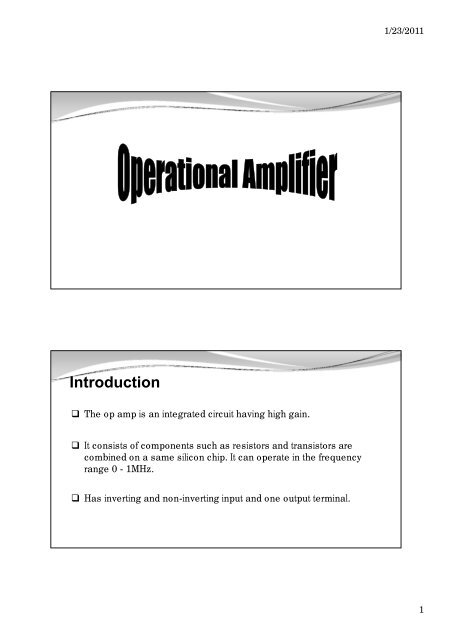
1/23/2011<strong>Introduction</strong>There are four configurations of differential amplifier in the op-ampcircuit.1. Double ended input, balance output.2. Double ended input, unbalance output.3. Single ended input, balance output.4. Single ended input, unbalance output.17Double ended input, balance output.9
1/23/2011Double ended input, unbalance output.Single ended input, balance output10
1/23/2011Single ended input, unbalance output.DEFFERENTIATE THE CONFIGURATIONEach configuration is categories based on several factors:1. Input signal quantity that use in circuit connection; Input : 2 input signal is used, so it is called 2 input Input: 1 input signal is used, so it is called single input.2. How output voltage being measured. If the voltage is measured between 2 collectors, the output will bebalance. If the voltage is measured at a collector and refer to ground, the outputwill not balance.2211
1/23/2011OP AMP INTERNAL BLOCK DIAGRAMConsist of 3 stages:Stage 1 –Stage 2 –Stage 3 –input stagecentre stageOutPput stageIt is designed in 3 stages to avoid problem when the input signal is weakand avoid from noise such as static interference, signal interference frompower supply.23InvertinginputNoninvertinginputDifferentialinput stagewith high inputimpedanceCentreamplifierstageOutput stagewith low outputimpedanceO/pBlock diagram of operational amplifier2412
1/23/2011High Input Impedance Differential Amplifier2 input, balance output.High impedance to each input signalLow gain to Common Mode Rejection Ratio(CMRR) such as humming and noise.High gain to useful signal25High Input Impedance Differential Amplifier (cont...)Reduce offset input voltageReduce ‘drift’ in circuit by using direct coupling.‘Drift’ is undesired signal that amplified togetherwith useful signalThis level most important because theimpedance for input is set and CMRR andoffset voltage is reduced.13
1/23/2011High Gain Voltage Amplifier2 input, balance output.High voltage gainHigh drive current gain to trigger outputand not burden to input.27Low Output impedance Differential AmplifierKnown as class B push pull amplifier @ push pullemitter follower.Consist of single input-balance outputAct as buffer to connect 2nd level and outputamplifier differential amplifier not affected by load.2814
1/23/2011Low Output impedance Differential Amplifier (Cont.....)Produce enough current to drive loadat output terminalHas low output impedance.Internal circuit diagram of Operational AmplifierV ccI/PQ1Q2Q4Q5D1D2Q7O/PI/PQ3Q8Q6Differential input stage Centre stage Output stage3015
1/23/2011Consist of 4 cascade amplifier.Differential amplifier with ‘Double ended output’A v1 formed by Q 1 and Q 2 while Q 3 is used as‘constant-current’ terminal for supply ‘highcommon mode rejection’Q 3 is stable from temperature effect by 2 resistorsand 2 diodes.Differential amplifier with single ended output Output from differential amplifier Q 1 and Q 2will trigger both Q 4 and Q 5 Q 4 and Q 5 have emitter source.Single ended output from second pair (fromQ 5 ) will trigger output stage through Q 6 .16
1/23/2011Feedback resistance for stable the output voltagerefers to ground.Q 7 and Q 8 operation as phase splitter for givemaximum voltage oscillation (almost same assupply voltage for minimize output impedance)Transistor Q 8 will amplify the signal.TERM and DEFINITIONObjective:To explain the meaning of the term / terminology that often usedin operational amplifiers:1. Open loop gain2. Common mode gain3. Offset Voltage4. Offset Current5. Virtual Ground3417
1/23/2011Open Loop Gain(A OL )• Amplifier gain without feedback• A OL = beacuse V o >> V id .+V ccV OV id-+-V cc• V id normally too small and practically can assume no different betweeninverting and non inverting.35Common Mode Gain, A CMThe gain when both input terminal have same signal Should be when V id =0, V o = 0 Practically, when Vo have value A cm will have small value.Common mode gain usually expressed as aCommon ModeRejection Ratio - CMRR, where.3618
1/23/2011Common Mode Gain, (A CM ) – cont... Normally A cm
1/23/2011Offset CurrentCaused by difference in bias currents are needed by both inputtransistors in the Op-Amp.Due to the imperfect matching between (current gain) of theinput stage transistors.I os = I B1 -I B24039Virtual GroundBoth the op amp input terminals are often referred to as thevirtual groundThis occurs because the current and voltage at both terminals isvery low when compared to current and voltage on the other,then it is called a virtual ground point.Virtual Ground is understood as the point at which the currentflow and voltage at that point is zero.20
1/23/2011Maximum rating for Op-Amp Op amp will damage if the maximum rate is exceeded :Power supply ±18V Operating temperature range, 0-700CInput voltage, maximum different between +ve and –ve terminal : 30VCommon mode input voltage, 12V, at power supply 15VInternal power dissipation, 310mW Saving temperature range, 55-1250CComparison of Operational Amplifier CharacteristicIdeal CharacteristicReal CharacteristicInfinite open loop gain Open loop gain = 200000-500000Infinite input impedance Z i = infiniteZero output impedance, Z out = 0Input impedance, Z i = 2 M - 5 MLow output impedance, Z out = 754221
1/23/2011Comparison of Operational Amplifier CharacteristicIdeal CharacteristicPerfect balance Q1 = Q2Zero offset VoltageZero offset currentFeatures that do not drift withtemperatureinfinite bandwidthReal Characteristic Q1 ≠ Q2Min offset voltage = 2 mvMin offset current = 100 nABeta drift with temperatureBandwidth = 1 Mhz43Advantages of Operational AmplifierSmall sizeHigh reliablityLower priceCan operate at low temperature rangeHave low voltage and current offset.4422
1/23/2011Advantages of Operational Amplifier - Cont.......Can be amplified small signalCan be use as analog computer equivalent circuit such as:summing, divider, integrator, differentialWaveform generatorActive filtercomparator454623
1/23/2011INTRODUCTIONTimer 555 is very stable integrated circuit. The timernormally used to generate the accurate delay time andalso generate oscillations.Basically, the timer 555 operates in two modes:-1. Monostable Multivibrator2. Astable Multivibrator24
1/23/2011PIN CONFIGURATION1 – ground2 - trigger3 - output4 - reset5 - voltage controlled6 - threshold voltage7 – Discharge8 – Supply voltage (v cc )Pin 1 : GroundConnected to groundPin 2: TriggerIt is used to trigger voltage for the comparator 2 to compare with .Output on pin 3 depending on the pulse of the trigger pin 2 signalPin 3 : OutputTerminal to be connected to load25
1/23/2011Pin 4 : ResetUsed to reset the output to its original condition or the initialconditions. This allows the output period T is shortened. Whennot in use, this pin is connected to +Vcc to prevent falsetriggeringPin 5 : Controlled VoltageIt is used to control the threshold voltage and the noise servesas a diverter if the capacitor is connected to earth through thispin. In monostable and astable mode, this pin is usuallyconnected to ground through a capacitor 0.01µFPin 6 : Threshold voltageFunction to set flip-flop and determine the level of voltage in the circuit.Pin 7: Discharge PinFunction to discharge the voltage on the capacitor when the timerinternal transistor is ONPin 8: Pin Bekalan+V CC (5 to 18V)26
1/23/2011LITAR DALAMANInternal section of timer consist of:-a) Voltage divider resistorb) 2 comparatorsc) SR Flip-Flopd) Switching transistore) Power supply 5V – 18V27
1/23/2011MONOSTABIL MULTIVIBRATORMONOSTABIL MULTIVIBRATOR28
1/23/2011OPERATIONAL PRINCIPLEAssume that the output pin 3 is in the LOW state at first. Thecircuit is in stable condition, at present transistor Q1 is ON.Capacitor C will shorted to ground. When the negative edge of the pulse applied to pin 2,transistor Q1 is OFF. Capacitor C will start charging towardthe + Vcc through a resistor RA, the timer output is HIGH.When the voltage on the capacitor C reaches the value 2 3the output will be set to LOW state.,29
1/23/2011At the same time, the output flip-flop will cause Q1 will be ON.Capacitor C will discharge through transistor Q1. Monostabiloutput will remain LOW until the trigger pulse applied to pin 2. Thiscycle is repeated. The length of time the output is in the "HIGH" is, T H = 1.11(RC)While the output frequency is equal to the frequency of triggeringsignals.ASTABLE MULTIVIBRATOR30
1/23/2011Astable MultivibratorOPERATIONAL PRINCIPLE Assume that the output is at HIGH state at first. At this time thetransistor Q 1 is OFF. Capacitor C will start charging toward thepositive values through resistor R A and R B . When the voltage of thecapacitor C reaches the value 2 , comparator 1 will trigger the3flip-flop and the output changes from HIGH to LOW At this point the transistor Q1 will be ON. Capacitor C willdischarge through transistor Q1 and resistor RB. When the voltageon the capacitor C reaches the value of the output 1 .3Comparator 2 will trigger the flip-flop so that the timer the outputbecomes HIGH. This cycle will repeat.31
1/23/2011 This situation can be observed in the output diagram shownbelow. Capacitor output will discharge between 2 to 1 ,3 3this time is the same as the timer the output is at HIGH state.Voltage across capacitor and at pin 3 (Output terminal)32
1/23/2011Discharging time is given by (time of output in HIGH state):TH = 0.693 (RA + RB) CDischarge time is given by (time of output in LOW state):TL = 0.693 RB CTotal period is:-T = TH + TL= 0.693(RA + 2RB)COutput frequency : = 1% Duty cycle: D ( ratio of high state to period of pulse)33
1/23/2011ASTABLE MULTIVIBRATORExample:A 555 timer connected as a astable multivibrator, if given a R A = 2.2KΩ,R B = 3.9KΩ and C = C 1 = 0.1μF. Draw the waveforms at pin 6 or pin 2 andpin 3. calculate the T H , T L output frequency, f, and % duty cycle, %DT.34
1/23/2011Example:-a) For an op amp, define the following termsi) Offset currentii) Common mode rejection ratiob) State the functions of pins 1, 2 and 4 of timer 555 is operated in amonostable modec) A 555 timer circuit is connected in astable mode with the values of thefollowing components: -R A = 2k, R B = 4k and C = 0.1μF. Calculate,T H , T L and T, frequency, f, Percentage of duty cycle, %DT. Draw the outputwaveform.Januari 2009a) Draw and label a complete symbol of the op-amp.b) Give FOUR (4) differences between ideal characteristics andactual characteristics of the op-ampc) i. Sketch the waveform on pin 2 and pin 3 of timer 555 when it isoperated in the astable mode.ii. A 555 timer connected in the unstable mode and given R A = 2.3k,R B = 4.6k and C = 0.1μF. Calculate T H , T L , frequency, f andpercentage of duty cycle of output waveform.Januari 201035
1/23/2011a) State the functions of the op-ampb) Draw a block diagram of an op-ampc) Definei. Offset voltageii. Virtual groundd) For a given circuit,calculate the T H , T L , f,and %DTJulai 200936