Characterization of 5Gsps ADC Demux 1:2 Board - CASPER
Characterization of 5Gsps ADC Demux 1:2 Board - CASPER
Characterization of 5Gsps ADC Demux 1:2 Board - CASPER

Create successful ePaper yourself
Turn your PDF publications into a flip-book with our unique Google optimized e-Paper software.
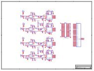
<strong>Characterization</strong> <strong>of</strong> <strong>5Gsps</strong> <strong>ADC</strong> <strong>Demux</strong> 1:2<strong>Board</strong>Homin Jiang a , Howard Liu a , Kim Guzzino a , Derek Kubo a , CT Li a , Kevin Lo a , Ray Chang a , Arthur Tsai bDate—Dec. 24 2011. Lab: ASIAA, Taipei.AI. INTRODUCTIONSIAA, the Academia Sinica Institute <strong>of</strong> Astronomy andAstrophysics, has developed a 5 Giga sample persecond (<strong>5Gsps</strong>) Analog to Digital (<strong>ADC</strong>) Printed Circuit<strong>Board</strong> (PCB) for the <strong>CASPER</strong>[1] community by employingan e2V‘s EV8AQ160 <strong>ADC</strong> chip[1]. Analog data from thesky, passes thru the balun filters, and is digitalized by thechip, then the <strong>ADC</strong> board outputs the digitized data to theROACH1 or ROACH2[1] board via the Z-DOK connector,that is the standard process using the <strong>CASPER</strong> toolflow.At the time <strong>of</strong> <strong>ADC</strong> board development, only ROACH 1was available. The maximum allowed global clockfrequency <strong>of</strong> ROACH 1 is 450MHz, which is the limitation<strong>of</strong> ROACH board. With the 450MHz limitation, the <strong>ADC</strong>clock can be driven to 1.8GHz only. To break thru thelimitation, we made the other version <strong>of</strong> PCB which is called<strong>Demux</strong> 1:2 <strong>ADC</strong> board. This board sacrifices the lower 4 bit<strong>of</strong> each sample. The disadvantage <strong>of</strong> the <strong>Demux</strong> 1:2 board is,it has only 4 bits because it is limited by the number <strong>of</strong> pins<strong>of</strong> the ZDOK connector. On the other hand, the output data<strong>of</strong> the <strong>Demux</strong> 1:2 board is demultiplexed by 8. This allowsthe use <strong>of</strong> all <strong>of</strong> the ZDOK pins at half the <strong>Demux</strong> 1:1 rate.Therefore the clock rate <strong>of</strong> <strong>Demux</strong> 1:2 board is half <strong>of</strong><strong>Demux</strong> 1:1 board. The system clock <strong>of</strong> ROACH boardusually aligns the clock signal <strong>of</strong> the <strong>ADC</strong> board tominimize the spurious harmonics. While the <strong>Demux</strong> 1:2<strong>ADC</strong> board is driven up to 2.5GHz, With thede-multiplexing factor <strong>of</strong> 8, the system clock is only312.5MHz, which is within the operating range <strong>of</strong> theROACH1 board.In this article, mainly the <strong>Demux</strong> 1:2 version <strong>of</strong> the <strong>5Gsps</strong><strong>ADC</strong> board was under test for the characterization. The<strong>Demux</strong> 1:1 board was examined only for the impedance <strong>of</strong>the clock traces. Passive and active tests were carried out tohave more information about the board. Passive tests tell theimpedance <strong>of</strong> the PCB traces, insertion and reflection loss <strong>of</strong>the input path and the connected passive components. Activemeasurements tell the typical <strong>ADC</strong> characterization, such asEffective Number Of Bits (ENOB), Signal to Noise andDistortion (SINAD) and Spurious Free Dynamic Range(SFDR) [3].II. PASSIVE MEASUREMENT OF INPUT BALUNSDuring S21 transmission test, two pigtail UT-047 wireswith two SMA connectors were soldered to pin A7 and pinA8 individually. The SMA connector to A7 was connectedto an Agilent PNA-X N5245A Network Analyzer. The SMAconnector at A8 was terminated with a 50 ohm load.Physical setup is depicted in Fig.2. The blue line in Fig.3shows the transmission loss <strong>of</strong> the 2 balun configuration andred line shows the transmission loss <strong>of</strong> the 3 balunconfiguration. The baluns, CX-2156[4] by Pulse, used in theinput port contributed 0.4dB transmission loss each, for the 2balun configuration, there is 0.8 dB transmission loss in total.From the plot, it can be easily distinguished that the 2 balunsconfiguration has better transmission performance.A 100 ohms termination resistor is placed between pin A7Fig.1. Input schematic <strong>of</strong> <strong>ADC</strong> board. There are 3 baluns on the schematic,L1, L2 and L3 for limiting the input signal in the range <strong>of</strong> 2.5GHz. Inputsignal goes thru those baluns, crosses zero ohm resistor, R1 and R3, thenpasses thru the capacitors <strong>of</strong> 10n value, C1 and C2, enter the input pins <strong>of</strong><strong>ADC</strong> chip, A7 and A8. Two termination resistors R6 and R7 on thisschematic are not populated.a: The authors are with the Academia Sinica Institute <strong>of</strong> Astronomyand Astrophysics, P.O. Box 23-141, Taipei, 106, Taiwan. (phone:886-2-23665347; fax: 886-2-23677849; e-mail:homin@asiaa.sinica.edu.tw).Fig. 2. Bare board with a two balun input configuration under test fortransmission performance.
ProbeProbeVIAVIAOPEN,on ZDOK sideOPEN,but add ZDOKsFig. 7. Impedance <strong>of</strong> <strong>Demux</strong> 1 :2 board without ZDOK.traces <strong>of</strong> <strong>Demux</strong> 1:1 board, is smaller than that <strong>of</strong> the <strong>Demux</strong>1:2 board. The measurement results do not reveal theproblem that was reported concerning the <strong>Demux</strong> 1:1 board.Fig. 7 shows the impedance <strong>of</strong> <strong>Demux</strong> 1:2 board withoutZDOK connector on it. The peak between the peak <strong>of</strong>“Probe” and the valley <strong>of</strong> “VIA” is caused by the pair <strong>of</strong>serpentine paths, which is to equalize the path lengthsbetween the A and C clock pairs. The magnitude <strong>of</strong> abruptimpedance by the serpentine clock traces is almost the sameas the impedance valley caused by the thru hole.Fig. 8 and Fig. 9 show the impedance <strong>of</strong> the <strong>Demux</strong> 1:1and the <strong>Demux</strong> 1:2 board with ZDOK connectors installedindividually. The impedance mismatch by the ZDOK andthe thru hole are more severe than the clock traces.ProbeFig. 9. Dmux 1 :2 board with ZDOK installed. Black and red line bothrepresent the resistance <strong>of</strong> the pair <strong>of</strong> differential line repectively. Thegreen line is the average resistance <strong>of</strong> the pair <strong>of</strong> differential line. Thescale <strong>of</strong> Y axis is 20 ohm per grid, the ideal resistance is at the center <strong>of</strong> Yaxis,i.e. 100 ohmNonlinearity (DNL), a low power noise was added to thecarrier. A 2 GHz bandwidth noise source was attenuated by30dB to the carrier, passed thru a low pass filter, and thencombined with the CW carrier by a combiner. At the end, thedithered carrier was sent to the <strong>5Gsps</strong> <strong>ADC</strong> board which wasthe device under test.The clock frequency was fixed at 2500MHz by employingan Agilent 83630 synthesizer at 0dBm. The CW signal wasprovided by another Agilent 83630 synthesizer, at -5dBm,the value was selected to avoid saturation <strong>of</strong> <strong>ADC</strong> level.To have the spectrum for analysis, the Fast FourierTransform (FFT) was performed in Matlab. The number <strong>of</strong>sample points is 16384, that leads to the process gain <strong>of</strong>39.13 dB as equation (1) shows:MPr ocessGain 10Log() (1)2Where M is the number <strong>of</strong> samples.VIAOPEN,but add ZDOKsFig. 8. Impedance <strong>of</strong> Dmux 1 :1 board with ZDOK.IV. SFDR MEASUREMENTThe input frequency <strong>of</strong> Continuous Wave (CW) signalwas properly chosen to have the pure monotonic signal righton the center <strong>of</strong> spectral bin. To avoid artifacts <strong>of</strong> thequantization noise correlation[4], or the effect <strong>of</strong> DifferentialSetup <strong>of</strong> the active measurement such as SFDR, SINADand ENOB is that a <strong>5Gsps</strong> <strong>Demux</strong> 1:2 <strong>ADC</strong> board wasplugged in the ZDOK 0 connector <strong>of</strong> a ROACH 1 board.Inside the ROACH board, a simple model file was running.The model had a snap block capturing the digitized datafrom the <strong>ADC</strong> board, then saved it in the Block RAM(BRAM).[6][7] A Python program was running in thePersonal Computer (PC) pipelined the data in the BRAM tothe PC and saved the data to the hard drive. The testconductor retrieved the data files and analyzed with Matlab.Because the <strong>Demux</strong> 1:2 was specifically designed to meetthe limitation <strong>of</strong> ZDOK’s pins by discarding the 4 leastsignificant bits, there is no information <strong>of</strong> those 4 bits fromthe board. The full scale <strong>of</strong> 4 bits input can’t be converted tothe full scale input <strong>of</strong> the <strong>ADC</strong> chip which is ± 0.5V directly.To avoid the ambiguity, the parameters in the rest <strong>of</strong> this
article are all respect to the carrier only.As illustrated by Fig. 10, the SFDR is the power <strong>of</strong> carrierto the power <strong>of</strong> the strongest harmonic. Fig. 11 depicts thatthe SFDR <strong>of</strong> <strong>Demux</strong> 1:2 in the input range <strong>of</strong> 100MHz to2400MHz. The SFDR values are around 35dB at lowfrequency region, and the values are down to 25 dB at highfrequency region.V. SINAD MEASUREMENTSINAD as its name, comprises two components, signal tonoise (SNR) and signal to distortion (THD). The typicalmethod to calculate these two values is by gettinginformation from the spectrum. SNR is calculated bysubtracting the noise floor and the process gain from thepower <strong>of</strong> carrier as Fig. 10 demonstrates.The top 5 harmonic tones were picked and summed as thepower <strong>of</strong> Distortion (D). Subtracting the power <strong>of</strong> top fiveharmonics from the carrier (S) power, the Total HarmonicDistortion (THD) can be derived. Combine the SNR andTHD, the SINAD parameter can be derived as the equation(2) shows: S SNR 10log N S THD 10log D S SINAD 10log N D (2)Once there is SINAD value, the ENOB can be deriveddirectly using equation (3): Fullscale _ AmplitudeSINAD 1.76dB 20Log10 Input_AmplitudeENOB 6.02With two values <strong>of</strong> SINAD from previous section, we canderive two ENOB correspondingly. Another approach tocharacterize the ENOB <strong>of</strong> <strong>ADC</strong> board is performed by sinewave curve fitting.[3] Curve fitting tool called “cftool” byMatlab [8] is employed to perform this characterization.“cftool” fitted the data set according to the sine wave asequation (4) shows. In the ideal case, the CW input signalsare pure sine waves without <strong>of</strong>fset. Thus, 4 parameters <strong>of</strong>fitting the curve as equation (4) shows, is used to fit theamplitude, phase, frequency and <strong>of</strong>fset:F( x)a1sin( b1x c1) d1 (4)After fitting, it generates measures <strong>of</strong> the goodness <strong>of</strong> fit.The key parameter is the Sum <strong>of</strong> Squares Due to Error. Thisstatistic measures the total deviation <strong>of</strong> the response valuesfrom the fit to the response values. It is also called thesummed square <strong>of</strong> residuals and is usually labeled as SSE. Avalue closer to 0 indicates that the model has a smallerrandom error component, and that the fit will be more usefulfor prediction. The SSE measure includes errors due to(3)Where N is the power <strong>of</strong> noises.To avoid saturation, the input power was selected around1 bit under the full scale. The ENOB has to be compensateddue to the loss <strong>of</strong> the input power by equation (4). We inputthe amplitude around the half <strong>of</strong> the full scale. The ratio is15/8, 15 is the full scale <strong>of</strong> 4 bits.Another more straightforward method to derive theSINAD is by using s<strong>of</strong>tware tools, such as Matlab, in thiswork. The process is as follows, search the entire spectrum,locate the bin <strong>of</strong> carrier, sum the power <strong>of</strong> carrier withnearby spectral bins as the power <strong>of</strong> signal. Also sum all thepower <strong>of</strong> every spectral bin as the total power <strong>of</strong> thespectrum. Subtract the total power <strong>of</strong> spectrum to the power<strong>of</strong> carrier, leaves the power <strong>of</strong> noise and distortion. Dividethe power <strong>of</strong> signal by the power <strong>of</strong> noise and distortion asequation (2) shows.Because all the harmonics are taken into account, theSINAD obtained by s<strong>of</strong>tware method is a little bit worsethan it is obtained from the plot.VI. ENOB BY 3 METHODSFig. 10. Typical SFDR, SINAD measurement.Integral Non-Linearity (INL), DNL, missing codes, jitterand noises. Note that the curve fitting method is peformed intime domain, consequently no spectral information can beFig. 11. SFDR <strong>of</strong> input frequency from 100MHz to 2400MHz..
generated such as THD and SINAD.In ideal case, there is square error <strong>of</strong> every sample. In theassumption <strong>of</strong> one bit least significant bit(LSB) ,that is 1/12.Compare the SSE by the curve fitting with the ideal squareerror <strong>of</strong> whole spectrum, the ENOB can be obtained byfollowing equation (5):QAENOBN LogQ2 T QQTA1638412SSEWhere 16384 is the number <strong>of</strong> samples in the work, N is thenumber <strong>of</strong> <strong>ADC</strong> bits. Q T is the theoretical N-bit RMSquantization error. Q A is the actual RMS error from best fitsine wave.The ENOB by curve fitting <strong>of</strong> this work is around 3.6 to3.9 bits as the dark blue curve illustrated in Fig. 13. Itconsiders the purity <strong>of</strong> the sine wave only, without takingthe input power level into consideration. The ENOB by thecurve fitting method has better numbers than the ones by theprevious two methods.VII. SUMMARYThe passive measurements in Section II and III haveshown that the layout <strong>of</strong> the <strong>Demux</strong> 1:2 PCB board ispromising. The 2 balun configuration has been adopted byASIAA to have better performance in high frequency end.The major interesting <strong>ADC</strong> characterization parameter,ENOB, has been approached by 3 methods. The typicalmethod by the spectrum plot has the ENOB in between.Reading the noise floor visually from the spectrum plot,could lead to worse flatness across the whole band. TheENOB by the s<strong>of</strong>tware program has the worst ENOB due totaking all the harmonics into account. In the other hand,because no human error is involved, it has the better flatnessall over the band. The ENOB by curve fitting has the bestENOB, but considers the purity <strong>of</strong> sine wave without regardto spectral characteristics.The typical method is also the most popular way for <strong>ADC</strong>characterization, the ENOB by the typical method is mostvaluable for comparison. The worst ENOB is around 2.5 bitsat the high frequency end, and the best ENOB is around 3.9bits at the lower part <strong>of</strong> the band.The other two key parameters <strong>of</strong> <strong>ADC</strong> characterization,SFDR and SINAD are also obtained by the typical methods.(5)VIII. FUTURE WORKAs the Roach2 becomes available at the end <strong>of</strong> 2011, wewould like to keep characterizing the other version <strong>of</strong> <strong>5Gsps</strong><strong>ADC</strong> board, i.e. <strong>Demux</strong> 1:1 board (full speed 8 bit) which isnot possible using the Roach 1 board.dBc43.532.521.5122201816141210891.691.6183183275275366366458458549549641641733733824824916916100710071099SINAD1099Fig. 12. Black represents the SINAD by typical method. Red linerepresents the SINAD calculated by Matlab program.ENOB1190119012821373MHzREFERENCES[1] casper.berkeley.edu[2] Data Sheet: EV8AQ160, e2V[3] Walt Kester, “Data Conversion Handbook, Analog Devices”,ISBN:0-7506-7841-0[4] Data Sheet. CX2156[5] Brannon, Brad, “ Overcoming Converter Nonlinearities withDither,” Application Note AN-410, Analog Devices, 1995.[6] Walt Kester," Taking the Mystery out <strong>of</strong> the Infamous Formula,SNR= 6.02N + 1.76dB," and Why You Should Care”,MT-001, Tutorial,Analog Devices.[7] Walt Kester,"Understand SINAD, ENOB, SNR, THD, THD+N, andSFDR so You Don’t Get Lost in the Noise Floor" MT-003, Tutorial,Analog Devices.[8] Matlab1465155716481740183119232014210621972289Fig. 13. Effective Number <strong>of</strong> Bits by 3 methods. Dark blue line representsthe ENOB by curve fitting. Light Blue line represents the ENOB bytypical method with compensation. The pink line represents the ENOBcalculated by Matlab program with compensation. Brown line representsthe ENOB by typical method without compensation. The yellow linerepresents the ENOB which is calculated by Matlab program withoutcompensation.1282MHz1373146515571648174018311923201421062197228923802380The board under test can digitalized input signals up to2.5GHz, the SFDR, SINAD and ENOB are reasonable for a4 bit test but worsen as the input frequency increases.