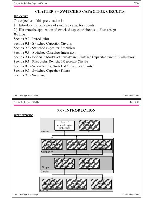
Switched Capacitor Circuits - Analog IC Design.org
Switched Capacitor Circuits - Analog IC Design.org
Switched Capacitor Circuits - Analog IC Design.org

You also want an ePaper? Increase the reach of your titles
YUMPU automatically turns print PDFs into web optimized ePapers that Google loves.
Chapter 9 – Section 1 (5/2/04) Page 9.1-10Analysis Methods for Two-Phase, Nonoverlapping Clocks - Cont’dTime-domain Relationships:The previous figure showed that,v*(t) = v o (t) + v e (t)where the superscript o denotes the odd phase (φ 1 ) and the superscript e denotes theeven phase (φ 2 ).For any given sample point, t = nT/2, the above may be expressed as⎛nT⎞v* ⎜ ⎟⎝ 2 = v o ⎛nT⎞⎜ ⎟⎠ n=1,2,3,4,5,6,··· ⎝ 2 ⎠ n=1,3,5,··· + v e ⎛nT⎞⎜ ⎟⎝ 2 ⎠ n=2,4,5,···z-domain Relationships:Consider the one-sided z-transform of a sequence, v(nT), defined as∞V(z) = Σn = 0 v(nT)z- n = v(0) + v(T)z - 1 + v(2T)z - 2 + ···for all z for which the series V(z) converges.Now, this equation can be expressed in the z-domain asV*(z) = V o (z) + V e (z) .The z-domain format for switched capacitor circuits will allow the analysis of transferfunctions.CMOS <strong>Analog</strong> Circuit <strong>Design</strong> © P.E. Allen - 2004Chapter 9 – Section 1 (5/2/04) Page 9.1-11Transfer Function Viewpoint of <strong>Switched</strong> <strong>Capacitor</strong> <strong>Circuits</strong>Input-output voltages of a general switched capacitor circuit in the z-domain.<strong>Switched</strong>o eo eV i (z) = V i (z) + V i (z) <strong>Capacitor</strong> V o(z) = V o(z) + V o(z)Circuit1 2Fig. 9.1-07z-domain transfer functions:H ij (z) = V o j (z)V i i(z)where i and j can be either e or o. For example, H oe (z) represents V e o (z)/ V o i (z) .Also, a transfer function, H(z) can be defined asH(z) = V o(z)V i (z) = Ve o(z) + V o o(z)V e i(z) + V o i(z) .CMOS <strong>Analog</strong> Circuit <strong>Design</strong> © P.E. Allen - 2004
Chapter 9 – Section 1 (5/2/04) Page 9.1-12Approach for Analyzing <strong>Switched</strong> <strong>Capacitor</strong> <strong>Circuits</strong>1.) Analyze the circuit in the time-domain during a selected phase period.2.) The resulting equations are based on q = Cv.3.) Analyze the following phase period carrying over the initial conditions from theprevious analysis.4.) Identify the time-domain equation that relates the desired voltage variables.5.) Convert this equation to the z-domain.6.) Solve for the desired z-domain transfer function.7.) Replace z by e jωT and examine the frequency response.CMOS <strong>Analog</strong> Circuit <strong>Design</strong> © P.E. Allen - 2004Chapter 9 – Section 1 (5/2/04) Page 9.1-13Example 9.1-3 - Analysis of a <strong>Switched</strong> <strong>Capacitor</strong>, First-order, Low pass FilterUse the above approach to find the z-domain transfer function of the first-order, lowpass switched capacitor circuit shown below. This circuit was developed by replacingthe resistor, R 1 , of the previous circuit with the parallel switched capacitor resistor circuit.The timing of the clocks is also shown. This timing is arbitrary and is used to assist theanalysis and does not change the result.1 2Solutionφ 1 : (n-1)T< t < (n-0.5)TEquivalent circuit:v 1 C C v 21<strong>Switched</strong> capacitor, low pass filter.C1 o eC 1 2 v (n- 32)Tv (n-1)T2o2 v 2(n-1)T2 1 2 1 2 tn- T23 n-1 n-2 1 n n+21 n+1Clock phasing for this example.Fig. 9.1-08C 2v 1 o e(n-1)T C 1v (n- 32 2)Tov 2(n-1)TEquivalent circuit.Simplified equivalent circuit.Fig. 9.1-09The voltage at the output (across C 2 ) is v o 2 (n-1)T = ve 2(n-3/2)T (1)CMOS <strong>Analog</strong> Circuit <strong>Design</strong> © P.E. Allen - 2004
Chapter 9 – Section 1 (5/2/04) Page 9.1-14Example 9.1-3 - Continuedφ 2 : (n-0.5)T< t < nTEquivalent circuit:C 112Fig. 9.1-10C 2v e 1(n-1/2)TC v e(n- 12 2)T1 ov (n-1)T vo(n-1)TThe output of this circuit can be expressed as the superposition of two voltagesources, v o 1 (n-1)T and v o 2 (n-1)T given asC 1v e ⎛ ⎞2 (n-1/2)T = ⎜ ⎟⎝ C 1 +C 2v o ⎛ ⎞⎠ 1 (n-1)T + ⎜ ⎟⎝ C 1 +C 2v o ⎠ 2 (n-1)T. (2)If we advance Eq. (1) by one full period, T, it can be rewritten asv o 2 (n)T = ve 2 (n-1/2)T. (3)Substituting, Eq. (3) into Eq. (2) yields the desired result given asv o ⎛2 (nT) = ⎜⎝C 1C 1 +C 2⎞⎟⎠v o ⎛1 (n-1)T + ⎜⎝C 2C 2⎞⎟⎠C 1 +C 2v o 2 (n-1)T. (4)CMOS <strong>Analog</strong> Circuit <strong>Design</strong> © P.E. Allen - 2004Chapter 9 – Section 1 (5/2/04) Page 9.1-15Example 9.1-3 - Continuedz-domain Analysis:The next step is to write the z-domain equivalent expression for Eq. (4). This can bedone term by term using the sequence shifting property given asv(n-n 1 )T ↔ z-n 1 V(z) . (5)The result isV o ⎛2(z) = ⎜⎝C 1C 1 +C 2⎞⎟⎠z -1 V o ⎛1(z) + ⎜⎝C 2⎞⎟⎠C 1 +C 2z -1 V o 2(z). (6)Finally, solving for V2 o(z)/Vo 1 (z) gives the desired z-domain transfer function for theswitched capacitor circuit of this example asH oo (z) = Vo 2(z) z -1V o 1(z) = ⎝C 1 +C 2 ⎠1 - z -1 ⎛ C 2⎞=⎜ ⎟⎝C 1 +C 2 ⎠⎛⎜C 1⎞⎟z -11 + α - αz -1 , where α = C 2C 1. (7)CMOS <strong>Analog</strong> Circuit <strong>Design</strong> © P.E. Allen - 2004
Chapter 9 – Section 1 (5/2/04) Page 9.1-16Discrete-Frequency Domain AnalysisRelationship between the continuous and discrete frequency domains:z = e jωTIllustration:Continuoustime frequencyresponsej= ∞= 0Discretetime frequencyresponse-1Imaginary Axis+j1= -∞r = 1= ∞ = 0+1 RealAxis= -∞Continuous Frequency Domain-j1Discrete Frequency DomainFig. 9.1-11CMOS <strong>Analog</strong> Circuit <strong>Design</strong> © P.E. Allen - 2004Chapter 9 – Section 1 (5/2/04) Page 9.1-17Example 9.1-4 - Frequency Response of Example 9.1-3Use the results of the previous example to find the magnitude and phase of thediscrete time frequency response for the switched capacitor circuit of Example 3.SolutionThe first step is to replace z in H oo (z) of Ex. 3 by e jωT . The result is given below aseH oo⎛⎝e ⎠ ⎞ =11+α-α e -jωT = (1+α)e jωT - α = 1(1+α)cos(ωT)- α + j(1+α)sin(ωT) (1)where we have used Eulers formula to replace e jωT by cos(ωT)+jsin(ωT). The magnitudeof Eq. (1) is found by taking the square root of the square of the real and imaginarycomponents of the denominator to give1⎪H ⎪ =(1+α) 2 cos 2 (ωT) - 2α(1+α)cos(ωT) + α 2 + (1+α) 2 sin 2 (ωT)=1(1+α) 2 [cos 2 (ωT)+sin 2 (ωT)]+α 2 -2α(1+α)cos(ωT)=11+2α+α 2 -2α(1+α)cos(ωT) = 11+2α(1+α)(1-cos(ωT)) . (2)The phase shift of Eq. (1) is expressed as(1+α)sin(ωT)Arg⎡⎣ H oo ⎦⎤ = - tan -1 ⎢⎢⎡ ⎣(1+α)cos(ωT)-α ⎦ ⎥⎥⎤ sin(ωT)tan-1 ⎢⎢⎡ α⎣cos(ωT) - 1+α⎦ ⎥⎥⎤(3)CMOS <strong>Analog</strong> Circuit <strong>Design</strong> © P.E. Allen - 2004
Chapter 9 – Section 1 (5/2/04) Page 9.1-18The Oversampling AssumptionThe oversampling assumption is simply to assume that f signal
Chapter 9 – Section 1 (5/2/04) Page 9.1-20Example 9.1-5 - ContinuedFrequency Response of the First-order, <strong>Switched</strong> <strong>Capacitor</strong>, Low Pass Circuit:1100Magnitude0.8500.707Arg[H oo (e jωT )]0.6|H oo (e jωT ω = 1/τ 1)|00.4-500.2Arg[H(jω)]ω = 1/τ 1 |H(jω)|0-1000 0.2 0.4 0.6 0.8 10 0.2 0.4 0.6 0.8 1ω/ω c ω/ω cFig. 9.1-12Better results would be obtained if f c > 20kHz.Phase Shift (Degrees)CMOS <strong>Analog</strong> Circuit <strong>Design</strong> © P.E. Allen - 2004Chapter 9 – Section 1 (5/2/04) Page 9.1-21SUMMARY• Resistance emulation is the replacement of continuous time resistors with switchedcapacitor approximations- Parallel switched capacitor resistor emulation- Series switched capacitor resistor emulation- Series-parallel switched capacitor resistor emulation- Bilinear switched capacitor resistor emulation• Time constant accuracy of switched capacitor circuits is proportional to thecapacitance ratio and the clock frequency• Analysis of switched capacitor circuits includes the following steps:1.) Analyze the circuit in the time-domain during a selected phase period.2.) The resulting equations are based on q = Cv.3.) Analyze the following phase period carrying over the initial conditions from theprevious analysis.4.) Identify the time-domain equation that relates the desired voltage variables.5.) Convert this equation to the z-domain.6.) Solve for the desired z-domain transfer function.7.) Replace z by e jωT and examine the frequency response.CMOS <strong>Analog</strong> Circuit <strong>Design</strong> © P.E. Allen - 2004
Chapter 9 – Section 2 (5/2/04) Page 9.2-1SECTION 9.2 – SWITCHED CAPACITOR AMPLIFIERSCONTINUOUS TIME AMPLIFIERSInverting and Noninverting AmplifiersR 1 R 2 vOUTR 1 R 2 vOUTv INFig. 9.2-01--v IN +Gain and GB = ∞:V outV in= R 1+R 2R 1Gain ≠ ∞, GB = ∞:A vd (0)R 1V out (s)V in (s) = ⎜ ⎜ ⎛ R 1 +R 2⎝ ⎠ ⎟ ⎟ ⎞ R 1 +R 2R 11 + A vd(0)R 1R 1 +R 2Gain ≠ ∞, GB ≠ ∞:GB·R 1V out (s)V in (s) = ⎜ ⎜ ⎛ R 1 +R 2⎝ ⎠ ⎟ ⎟ ⎞ R 1 +R 2⎛R R 1s + GB·R ⎜ 1 +R 2⎞ ω⎟ H1= ⎜ ⎟⎝ R 1 ⎠ s+ω HR 1 +R 2V outV in= - R 2R 1R 1 A vd (0)V out (s)V in (s) = - ⎜ ⎜ ⎛ R 2⎝ ⎠ ⎟ ⎟ ⎞ R 1 +R 2R 11 + A vd(0)R 1R 1 +R 2GB·R 1V out (s)V in (s) = ⎜ ⎜ ⎛- R 2 R 1 +R 2⎝R 1⎠ ⎟ ⎟ ⎞⎛⎜s + GB·R 1R 1 +R 2=⎝⎜- R 2 ⎞R 1⎟⎟⎠ω Hs+ω H+CMOS <strong>Analog</strong> Circuit <strong>Design</strong> © P.E. Allen - 2004Chapter 9 – Section 2 (5/2/04) Page 9.2-2Example 9.2-1- Accuracy Limitation of Voltage Amplifiers due to a Finite VoltageGainAssume that the noninverting and inverting voltage amplifiers have been designed fora voltage gain of +10 and -10. If A vd (0) is 1000, find the actual voltage gains for eachamplifier.SolutionFor the noninverting amplifier, the ratio of R 2 /R 1 is 9.A vd (0)R 1 /(R 1 +R 2 ) = 10001+9 = 100.V out⎛100⎞∴ V in= 10 ⎜ ⎟⎝ 101 = 9.901 rather than 10.⎠For the inverting amplifier, the ratio of R 2 /R 1 is 10.A vd (0)R 1R 1 +R 2= 10001+10 = 90.909∴V out⎛ 90.909V in= -(10) ⎜⎝ 1+90.909 = - 9.891 rather than -10.⎞⎟⎠CMOS <strong>Analog</strong> Circuit <strong>Design</strong> © P.E. Allen - 2004
Chapter 9 – Section 2 (5/2/04) Page 9.2-3Example 9.2-2 - -3dB Frequency of Voltage Amplifiers due to Finite Unity-GainbandwidthAssume that the noninverting and inverting voltage amplifiers have been designed fora voltage gain of +1 and -1. If the unity-gainbandwidth, GB, of the op amps are2πMrads/sec, find the upper -3dB frequency for each amplifier.SolutionIn both cases, the upper -3dB frequency is given byω H = GB·R 1R 1 +R 2For the noninverting amplifier with an ideal gain of +1, the value of R 2 /R 1 is zero.∴ ω H = GB = 2π Mrads/sec (1MHz)For the inverting amplifier with an ideal gain of -1, the value of R 2 /R 1 is one.∴ ω H = GB·11+1 = GB2 = π Mrads/sec (500kHz)CMOS <strong>Analog</strong> Circuit <strong>Design</strong> © P.E. Allen - 2004Chapter 9 – Section 2 (5/2/04) Page 9.2-4CHARGE AMPLIFIERSNoninverting and Inverting Charge AmplifiersC 1 C 2vOUTv INC 1 C 2vOUT--v IN++Gain and GB = ∞:V outV in= C 1+C 2C 2Gain ≠ ∞, GB = ∞:Noninverting Charge AmplifierA vd (0)C 2V out⎛C 1 +C 2⎞ C 1 +C 2V = ⎜ ⎟in ⎝ C 2 ⎠1 + A vd(0)C 2C 1 +C 2Gain ≠ ∞, GB ≠ ∞:GB·C 2V outV in= ⎜ ⎛C1+C 2C 1 +C 2⎝ C ⎠ ⎟⎞2s + GB·C 2C 1 +C 2Inverting Charge AmplifierV outV in= - C 1C 2A vd (0)C 2V out⎛V = ⎜ ⎟in ⎝- C 1 ⎞ C 1 +C 2C 2 ⎠1 + A vd(0)C 2C 1 +C 2GB·C 2V in= ⎜ ⎛⎝- C 1C 1 +C 2C ⎠ ⎟⎞2s + GB·C 2C 1 +C 2V outCMOS <strong>Analog</strong> Circuit <strong>Design</strong> © P.E. Allen - 2004
Chapter 9 – Section 2 (5/2/04) Page 9.2-5SWITCHED CAPACITOR AMPLIFIERSParallel <strong>Switched</strong> <strong>Capacitor</strong> Amplifierv in1 22+C 1v C1-1 2C-++-v C2v outv in1 2C 1+-v C1-+-1v C2+C 2v outInverting <strong>Switched</strong> <strong>Capacitor</strong> AmplifierAnalysis:Find the even-odd and the even-even z-domaintransfer function for the above switched capacitorinverting amplifier.φ 1 : (n -1)T < t < (n -0.5)Tandv o C1o(n -1)T = v (n -1)TinClockvC2 o (n -1)T = 0Modification to prevent open-loop operation2 1 2 1 2 tTn-1 n-2 1 n n+21 n+1phasing for this example.n- 3 2CMOS <strong>Analog</strong> Circuit <strong>Design</strong> © P.E. Allen - 2004Chapter 9 – Section 2 (5/2/04) Page 9.2-6Parallel <strong>Switched</strong> <strong>Capacitor</strong> Amplifier- Continuedφ 2 : (n -0.5)T < t < nTt = 0 v C2 = 0Equivalent circuit:- +From the simplifiedequivalent circuit wewrite,⎛C 1⎞vout e (n-1/2)T = - ⎜ ⎟⎝C 2v o⎠ in (n-1)TConverting to the z-domain gives,z -1/2 Vout e (z) = - ⎜⎝Multiplying by z 1/2 gives,V eout (z) = - ⎝⎛C 1⎞⎜ ⎟C 2 ⎠C 1⎛C 1⎞⎟C 2 ⎠2+voin(n-1)T-Equivalent circuit at the moment φ2 closes.z -1 V oin (z)z -1/ 2 V oin (z)vino (n-1)T-+Solving for the even-odd transfer function, H oe (z), gives, H oe (z) = V eout (z)V o-+ev out (n-1/2)Tin (z) = -⎜⎛⎝C 2z -1/ 2CMOS <strong>Analog</strong> Circuit <strong>Design</strong> © P.E. Allen - 2004+v C1C 1-v C2= 0 = 0 e- + - + vout (n-1/2)TC 2Simplified equivalent circuit.C 1⎠ ⎟⎞
Chapter 9 – Section 2 (5/2/04) Page 9.2-7Parallel <strong>Switched</strong> <strong>Capacitor</strong> Amplifier- ContinuedSolving for the even-even transfer function, H ee (z).Assume that the applied input signal, v o in (n-1)T, was unchanged during the previousφ 2 phase period(from t = (n-3/2)T to t = (n-1)T), thenv o in (n-1)T = v e in (n-3/2)Twhich givesVin(z) o = z -1/2 Vin(z) e .Substituting this relationship into H oe (z) givesorV e⎛⎜C 1⎞⎟⎟⎠out(z) = -⎜⎝ C z -1 V e 2in(z)H ee (z) = V eout(z)C 1⎠ ⎟ ⎟ ⎞Vin(z) e = -⎜ ⎜ ⎛⎝C 2z -1CMOS <strong>Analog</strong> Circuit <strong>Design</strong> © P.E. Allen - 2004Chapter 9 – Section 2 (5/2/04) Page 9.2-8Frequency Response of <strong>Switched</strong> <strong>Capacitor</strong> AmplifiersReplace z by e jωT .andH oe (e jωT ) = V out( ee jωT )Vout( ee jωT ) = -⎜ ⎜ ⎛⎝C 1⎠ ⎟ ⎟ ⎞C 2e -jωT/2H ee (e jωT ) = V out(e e jωT )Vout( oe jωT ) = - ⎛C 1⎞⎜ ⎟⎝C 2e -jωT⎠If C 1 /C 2 = R 2 /R 1 , then the magnitude response is identical to inverting unity gain amp.However, the phase shift of H oe (e jωT ) isArg[H oe (e jωT )] = ±180° - ωT/2and the phase shift of H ee (e jωT ) isArg[H ee (e jωT )] = ±180° - ωT.Comments:• The phase shift of the SC inverting amplifier has an excess linear phase delay.• When the frequency is equal to 0.5f c , this delay is 90°.• One must be careful when using switched capacitor circuits in a feedback loopbecause of the excess phase delay.CMOS <strong>Analog</strong> Circuit <strong>Design</strong> © P.E. Allen - 2004
Chapter 9 – Section 2 (5/2/04) Page 9.2-9Positive and Negative Transresistance Equivalent <strong>Circuits</strong>Transresistance circuits are two-port networks where the voltage across one portcontrols the current flowing between the ports. Typically, one of the ports is at zeropotential (virtual ground).<strong>Circuits</strong>:i 1 (t) v C (t) i 2 (t)i 1 (t) v C (t) i 2 (t)2 212v 1 (t)1C1v 1 (t)Positive Transresistance Realization.Analysis (Negative transresistance realization):R T = v 1(t)i 2 (t) = v 1i 2 (average)If we assume v 1 (t) is ≈ constant over one period of the clock, then we can writei 2 (average) = 1 T q 2 (T) - q 2 (T/2) Cv C (T) - Cv C (T/2)T ⌡⌠ i 2 (t)dt = T = T = -Cv 1TT/2C P C PNegative Transresistance Realization.C P2C1C PSubstituting this expression into the one above shows thatR T = -T/CSimilarly, it can be shown that the positive transresistance is T/C.These circuits are insensitive to the parasitic capacitances shown as dotted capacitors.CMOS <strong>Analog</strong> Circuit <strong>Design</strong> © P.E. Allen - 2004Chapter 9 – Section 2 (5/2/04) Page 9.2-10Noninverting Stray Insensitive <strong>Switched</strong> <strong>Capacitor</strong> AmplifierAnalysis:φ 1 : (n -1)T < t < (n -0.5)TThe voltages across each capacitor can be written asn-23vC1(n o -1)T = vin(n o -1)TandvC2(n o -1)T = vout(n o-1)T = 0 .v inv C1 (t)Cφ 2 : (n -0.5)T < t < nT12 1The voltage across C 2 isv eout(n -1/2)T = ⎝⎜V e⎛C 1⎞⎠⎛C 1⎞⎟C 2 ⎠v o in(n -1)T⎛C ⎜ 1⎞⎟⎟⎠out(z) = ⎜ ⎟⎝ C 2z -1/2 Vin(z) o → H oe (z) = ⎜ ⎝C 2z -1/2If the applied input signal, v o in(n -1)T, was unchanged during the previous φ 2 phase, then,V e⎛C 1⎞⎟C 2 ⎠out(z) = ⎜⎝z -1 Vin(z) e→ H ee (z) = ⎜⎛ ⎜ ⎝C 2 ⎠ ⎟⎟⎞ z -1Comments:• Excess phase of H oe (e jωT ) is -ωT/2 and for H ee (e jωT ) is -ωTCMOS <strong>Analog</strong> Circuit <strong>Design</strong> © P.E. Allen - 2004C 12 1 2 1 2 tTn-1 n-2 1 n n+21 n+1Clock phasing for this example.1 2Noninverting <strong>Switched</strong> <strong>Capacitor</strong> Voltage Amplifier.-+-1v C2+C 2v out
Chapter 9 – Section 2 (5/2/04) Page 9.2-11Inverting Stray Insensitive <strong>Switched</strong> <strong>Capacitor</strong> AmplifierAnalysis:φ 1 : (n -1)T < t < (n -0.5)TThe voltages across each capacitor can v in 2be written asandv o C1(n -1)T = 0vC2(n o -1)T = vout(n o-1)T = 0 .φ 2 : (n -0.5)T < t < nTThe voltage across C 2 isv eout(n -1/2)T = - ⎝⎜V eC 1⎞⎠⎛C 1⎞⎟C 2 ⎠out(z) = - ⎛⎜ ⎟⎝ C V e2in(z) →v ein(n -1/2)TH˚oe (z) = -⎝⎜Inverting <strong>Switched</strong> <strong>Capacitor</strong> Voltage Amplifier.⎛C ⎜ 1⎞⎟C ⎟ 2 ⎠v C1 (t)Comments:• The inverting switched capacitor amplifier has no excess phase delay.• There is no transfer of charge during φ 1 .1v C1 (t)C 112-+-1v C2+C 2v outCMOS <strong>Analog</strong> Circuit <strong>Design</strong> © P.E. Allen - 2004Chapter 9 – Section 2 (5/2/04) Page 9.2-12Example 9.2-3 - <strong>Design</strong> of a <strong>Switched</strong> <strong>Capacitor</strong> Summing Amplifier<strong>Design</strong> a switched capacitor summingamplifier using the stray insensitive transresistancecircuits to gives the output voltage during 1110C21vCthe φ 2 phase period that is equal to 10v 1 - 5v 2 ,2 1where v 1 and v 2 are held constant during a φ 2 -φ 1period and then resampled for the next period.5C-22vSolution2A possible solution is shown. Considering1 1+each of the inputs separately, we can write thatvo1 e (n-1/2)T = 10vo 1 (n-1)T (1)andvo2 e (n-1/2)T = -5ve 2 (n-1/2)T . (2)Because v o 1 (n-1)T = ve 1 (n-3/2)T, Eq. (1) can be rewritten asvo1 e (n-1/2)T = 10ve 1 (n-3/2)T . (3)Combining Eqs. (2) and (3) givesv e o (n-1/2)T = v o1 e (n-1/2)T + v o2 e (n-1/2)T = 10ve 1 (n-3/2)T - 5ve 2 (n-1/2)T . (4)orV e o (z) = 10z-1 V e 1 (z) - 5Ve 2 (z) . (5)v oCMOS <strong>Analog</strong> Circuit <strong>Design</strong> © P.E. Allen - 2004
Chapter 9 – Section 2 (5/2/04) Page 9.2-13NONIDEALITIES OF SWITCHED CAPACITOR CIRCUITSSwitchesCovered in Chapter 4.<strong>Capacitor</strong>sCovered in Chapter 2.CMOS <strong>Analog</strong> Circuit <strong>Design</strong> © P.E. Allen - 2004Chapter 9 – Section 2 (5/2/04) Page 9.2-14Example 9.2-4 – Influence of Clock Feedthrough on a Noninverting <strong>Switched</strong><strong>Capacitor</strong> AmplifierA noninverting, switchedcapacitor voltage amplifier is1shown. The switch overlapC OL C OLcapacitors, C OL are assumed to12be 100fF each and C 1 = C 2 = C OL C OL C OL C OL1pF. If the switches have a W= 1µm and L = 1µm and the v in- v M5v C (t)C2+ v outnonoverlapping clock of 0 to 5V M1M4Camplitude has a rate of rise and C 2OLC 1 C OLfall of ±0.5x10 9 -volts/second,2 M3 M2 1find+the actual value of theCoutput voltage when a 1VOLC OLsignal is applied to the input.Fig. 9.2-9SolutionWe will break this example into three time sequences. The first will be when φ 1 turnsoff (φ 1off ), the second when φ 2 turns on (φ 2on ), and the third when φ 2 turns off (φ 2off ).CMOS <strong>Analog</strong> Circuit <strong>Design</strong> © P.E. Allen - 2004
Chapter 9 – Section 2 (5/2/04) Page 9.2-15Example 9.2-4 – Continuedφ 1 turning offC OLM1: 12The value ofC VHT is given asOL C OL C OL C OLvv C (t)inV HT = 5V-1V-0.7V = 3.3VM1M4C OLC 1 C OLTherefore, the value of βV HT2/2C L is found as2 M3 M2 1βV HT22C L= 110x10 C OL-6(3.3)22x10-12 = 0.599x10 9 V/sec.This corresponds to the slow transition mode. Using the previous model gives⎛⎜220x10 ⎟V error = -18 +(0.5)(24.7)(10 -16 ) ⎞ π109·10-12⎜⎟⎝ 10 -12⎠ 2·110x10-6 - 220x10 -1810 -12 (1+1.4+0)= (0.001455)(3.779) - 220x10-6(2.4) = 5.498mV-0.528mV = 4.97mVM2:The value of VHT for M2 is given asV HT = 5V-0V-0.7V = 4.3VThe value of βV HT2/2C L is found asβV HT22C = 110x10 -6(4.3) 2L 2x10 -12 = 1.017x10 9 V/sec.1C OLM5- v C2+C 2-C OL+v outFig. 9.2-9CMOS <strong>Analog</strong> Circuit <strong>Design</strong> © P.E. Allen - 2004Chapter 9 – Section 2 (5/2/04) Page 9.2-16Example 9.2-4 – ContinuedTherefore, M2 is also in the slow transition mode. The error voltage is found as⎛⎜220x10 V error = -18 +(0.5)(24.7)(10 -16 ) ⎞⎜ ⎝10-12⎟⎟⎠π109·10-122·110x10-6 - 220x10 -1810-12 (0+1.4+0)= (0.001455)(3.779) - 220x10 -6 (1.4) = 5.498mV-0.308mV = 5.19mVTherefore, the net error on the C 1 capacitor at the end of the φ 1 phase isv C1 (φ 1off ) = 1.0 - 0.00497 + 0.00519 = 1.00022V1C OL C OLWe see that the influence of v in ≠ 0V is to cause the12Cfeedthrough from M1 and M2 not to cancel OL C OL C OL C OLM5vv C (t)completely.in- v C2+ v outM1M4CC 2M5:OLC 1 C OL -2 M3 +M2 1We must also consider the influence of M5 turning C OLC OLoff. In order to use the previous model for M5, we willFig. 9.2-9assume that feedthrough of M5 via a virtual ground is valid for the previous model givenfor feedthrough. Based on this assumption, M5 will have the same feedthrough as M2which is 5.19mV. This voltage error will left on C 2 at the end of the φ 1 and isv C2 (φ 1off ) = 0.00519V.CMOS <strong>Analog</strong> Circuit <strong>Design</strong> © P.E. Allen - 2004
Chapter 9 – Section 2 (5/2/04) Page 9.2-17Example 9.2-4 – Continuedφ 2 turning onC OL C OL12During the turn-on part of φ 2 , M3 and M4 will C OL C OL C OL C OLM5feedthrough onto C 1 and C 2 . However, it is easy to vv C (t)in- v C2+ v outshow that the influence of M3 and M4 will cancelM1M4CC 2OLC 1 C OLeach other for C 1 . Therefore, we need only consider2 M3 M2 1the feedthrough of M4 and its influence on C 2 .C OLC OLInterestingly enough, the feedthrough of M4 onto C 2Fig. 9.2-9is exactly equal and opposite to the previous feedthrough by M5. As a result, the value ofvoltage on C 2 after φ 2 has stabilized isv C2 (φ 2on ) = 0.00519V-0.00519V + C 1C 2v c1 (φ 1off ) = 1.00022Vφ 2 turning offFinally, as switch M4 turns off, there will be feedthrough onto C 2 . Since, M4 has oneof its terminals at 0V, the feedthrough is the same as before and is 5.19mV. The finalvoltage across C 2 , and therefore the output voltage v out , is given asv out (φ 2off ) = v C2 (φ 2off ) = 1.00022V + 0.00519V = 1.00541VIt is interesting to note that the last feedthrough has the most influence.CMOS <strong>Analog</strong> Circuit <strong>Design</strong> © P.E. Allen - 2004Chapter 9 – Section 2 (5/2/04) Page 9.2-18NONIDEAL OP AMPS - FINITE GAINFinite Amplifier GainConsider the noninverting switched capacitor amplifier during φ 2 :vo in(n-1)TThe output during φ 2 can be written as,-+C 1C 2ev out (n-1/2)Tev out (n-1/2)T -A vd (0)- +Op amp with finite+ value of A vd (0)Fig. 9.2-11vout(n e⎛C 1⎞-1/2)T = ⎜ ⎟⎝ C 2v o ⎛C 1 +C 2⎞ vout(n e-1/2)Tin(n -1)T + ⎜ ⎟⎠⎝ C 2 ⎠ A vd (0)Converting this to the z-domain and solving for the H oe (z) transfer function givesH oe (z) = V out(z)eVin(z) o = ⎛C 1⎞ ⎡ 1 ⎤⎜ ⎟⎝C 2z -1/2 ⎢⎥⎠ ⎢⎥⎣1 - C 1 + C 2.A vd (0)C 2⎦Comments:• The phase response is unaffected by the finite gain• A gain of 1000 gives a magnitude of 0.998 rather than 1.0.CMOS <strong>Analog</strong> Circuit <strong>Design</strong> © P.E. Allen - 2004
Chapter 9 – Section 2 (5/2/04) Page 9.2-19Nonideal Op Amps - Finite Bandwidth and Slew RateFinite GB:• In general the analysis is complicated. (We will provide more detail for integrators.)• The clock period, T, should be equal to or less that 10/GB.• The settling time of the op amp must be less that T/2.Slew Rate:• The slew rate of the op amp should be large enough so that the op amp can make afull swing within T/2.CMOS <strong>Analog</strong> Circuit <strong>Design</strong> © P.E. Allen - 2004Chapter 9 – Section 2 (5/2/04) Page 9.2-20SUMMARY• Continuous time amplifiers are influenced by the gain and gainbandwidth of the op amp• Charge amplifiers are also influenced by the gain and the gainbandwidth of the op amp• <strong>Switched</strong> capacitor amplifiers replace the resistors of the continuous time amplifier withswitched capacitor equivalents• The transresistor SC amplifiers can be inverting and noninverting with the positiveinput terminal of the op amp on ground• The nonidealities of the SC amplifier include:- Switches- <strong>Capacitor</strong>s- Op amp finite gain- Op amp finite GBCMOS <strong>Analog</strong> Circuit <strong>Design</strong> © P.E. Allen - 2004
Chapter 9 – Section 3 (5/2/04) Page 9.3-1SECTION 9.3 – SWITCHED CAPACITOR INTEGRATORSContinuous Time IntegratorsV inR 1C - 2 R R VoutVinR 1C 2V out---(a.)Inverter(a.) Noninverting and (b.) inverting continuous time integrators.Ideal Performance:Noninverting-Inverting-V out (jω)V in (jω) = 1jω R 1 C 2= ω Ijω = -jω I V out (jω)ωV in (jω) = -1jω R 1 C 2= -ω Ijω = jω IωFrequency Response:|V out (jω)/Vin(jω)|Arg[V out (jω)/V in (jω)](b.)+++40 dB90°20 dB0 dB-20 dB-40 dBω I100 10ω I ω I10ω I 100ω I0°log 10 ωω Ilog10 ω(a.)(b.)CMOS <strong>Analog</strong> Circuit <strong>Design</strong> © P.E. Allen - 2004Chapter 9 – Section 3 (5/2/04) Page 9.3-2Continuous Time Integrators - Nonideal PerformanceFinite Gain:A vd (s) sR 1 C 2A vd (s) (s/ω Ι )V out⎛ 1 ⎞ sR 1 C 2 + 1 ⎛V in= -⎜⎟⎝ sR 1 C 2 ⎠1 + A vd(s) sR 1 C = ⎜ ⎟2 ⎝- ω I ⎞ (s/ω Ι ) + 1s ⎠sR 1 C 2 +1 1 + A vd(s) (s/ω Ι )(s/ω Ι ) + 1where A vd (s) = A vd(0)ω as+ω = GB GBa s+ω ≈a sCase 1: s → 0 ⇒ A vd (s) = A vd (0) V out⇒Case 2: s → ∞ ⇒A vd (s) = GBsCase 3: 0 < s < ∞ ⇒ A vd (s) = ∞|V out (jω)/Vin(jω)|A vd (0) dB0 dBEq. (1)ω x1 =ω IA vd (0)ω IEq. (3)Eq. (2)ω x2 =⇒ V out⇒V ≈ - A vd (0) (1)in⎛GB⎞⎛ω I⎞V ≈ - ⎜ ⎟ ⎜ ⎟in ⎝ s ⎠ ⎝ s (2)⎠V outV ≈in- ω Is (3)GBlog10 ωArg[V out (jω)/V in (jω)]180°135°90°45°0°ω I10A vd (0) 10ωIA vd (0) GB1010GBω IA vd (0)GBlog 10 ωCMOS <strong>Analog</strong> Circuit <strong>Design</strong> © P.E. Allen - 2004
Chapter 9 – Section 3 (5/2/04) Page 9.3-3Example 9.3-1 - Frequency Range over which the Continuous Time Integrator isIdealFind the range of frequencies over which the continuous time integratorapproximates ideal behavior if A vd (0) and GB of the op amp are 1000 and 1MHz,respectively. Assume that ω I is 2000π radians/sec.SolutionThe “idealness” of an integrator is determined by how close the phase shift is to±90° (+90° for an inverting integrator and -90° for a noninverting integrator).The actual phase shift in the asymptotic plot of the integrator is approximately 6° above90° at the frequency 10ω I /A vd (0) and approximately 6° below 90° at GB /10.Assume for this example that a ±6° tolerance is satisfactory. The frequency range can befound by evaluating 10ω I /A vd (0) and GB/10.Therefore the range over which the integrator approximates ideal behavior is from 10Hzto 100kHz. This range will decrease as the phase tolerance is decreased.CMOS <strong>Analog</strong> Circuit <strong>Design</strong> © P.E. Allen - 2004Chapter 9 – Section 3 (5/2/04) Page 9.3-4Noninverting <strong>Switched</strong> <strong>Capacitor</strong> IntegratorAnalysis:φ 1 : (n -1)T < t < (n -0.5)Tvv1 C1 (t)vin2C2+ vThe voltage across each capacitor is+ -- outS1 S4 Cvc1(n-1)T o = vin(n-1)To -C 21S2 S32and+1vc2(n-1)T o = vout(n-1)T o.φ 2 : (n -0.5)T < t < n TNoninverting, stray insensitive integrator.Equivalent circuit:C 12-t = 0v C2 =vo in+ (n-1)T2t = 0v out(n-1)To- +-+C 2ev out (n-1/2)Tvo in-(n-1)T+v C1+= 0-C 1v out(n-1)To--+C 2+- +v C2 = 0ev out (n-1/2)TEquivalent circuit at the moment the φ2 switches close.Simplified equivalent circuit.We can write that, vout(n e-1/2)T = ⎛⎜⎝C 1C ⎠ ⎟⎞2v o in(n -1)T + v oout(n -1)TCMOS <strong>Analog</strong> Circuit <strong>Design</strong> © P.E. Allen - 2004
Chapter 9 – Section 3 (5/2/04) Page 9.3-5Noninverting <strong>Switched</strong> <strong>Capacitor</strong> Integrator - Continuedφ 1 : nT < t < (n + 0.5)TIf we advance one more phase period, i.e. t = (n)T to t = (n+1/2)T, we see that thevoltage at the output is unchanged. Thus, we may writevout(n)T o= vout(n-1/2)T e.Substituting this relationship into the previous gives the desired time relationshipexpressed as⎛C 1⎞vout(n)T o= ⎜ ⎟⎝ C 2vin(n o -1)T + vout(n o-1)T .⎠Transferring this equation to the z-domain gives,Vout(z) o ⎛C 1⎞= ⎜ ⎟⎝ C 2z -1 Vin(z) o + z -1 Vout(z) o→ H oo (z) = V out(z)o⎠V in(z) o = ⎛C 1⎞ z -1 ⎛C 1⎞ 1⎜ ⎟⎝C 2 ⎠ 1-z -1 = ⎜ ⎟⎝ C 2 ⎠ z-1Replacing z by e jω Τ gives,H oo (e jωΤ ) = V out( oe jωΤ ) ⎛C 1⎞⎛C 1⎞⎜ ⎟⎜ ⎟V in( o e jωΤ ) = 1⎝C 2 ⎠ e jωΤ -1 = e -jωΤ/2⎝C 2 ⎠ e jωΤ/2 - e -jωΤ/2Replacing e jωΤ/2 - e -jωΤ/2 by its equivalent trigonometric identity, the above becomesH oo (e jωΤ ) = V out(e o jωΤ ) ⎛C 1⎞ e -jωΤ/2 ⎛ωT⎞⎛ C 1⎞ ⎛ ωT/2 ⎞⎜ ⎟⎜ ⎟ ⎜ ⎟ ⎜⎟ e -jωΤ/2V o in( e jωΤ ) = ⎝C 2 ⎠j2 sin(ωT/2) ⎝ωT = ⎠ ⎝jωTC 2⎠ ⎝sin(ωT/2) ⎝ ⎛H oo (e jωT ) = (Ideal)x(Magnitude error)x(Phase error) where ω I = C 1 /TC 2 ⇒ Ideal = ω I /jω⎠⎠ ⎞CMOS <strong>Analog</strong> Circuit <strong>Design</strong> © P.E. Allen - 2004Chapter 9 – Section 3 (5/2/04) Page 9.3-6Example 9.3-2 - Comparison of a Continuous Time and <strong>Switched</strong> <strong>Capacitor</strong>IntegratorAssume that ω I is equal to 0.1ω c and plot the magnitude and phase response of thenoninverting continuous time and switched capacitor integrator from 0 to ω c .SolutionLetting ω I be 0.1ω c givesPlots:54321H(jω) =110jω/ω cMagnitudeand H oo (e jωΤ ⎛) = ⎜⎝|H oo (e jω T )|-200|H(jω)|ω I-250-300ω/ω c110jω/ω c0-50-100-150⎞ ⎛⎟ ⎜⎠ ⎝πω/ω csin(πω/ω c ) ⎛ ⎝Phase Shift (Degrees)⎞⎟⎠e -jπω/ωc⎠ ⎞Arg[H(jω)]Arg[H oo (e jω T )]00 0.2 0.4 0.6 0.8 1ω I0 0.2 0.4 ω/ω 0.6 0.8 1cCMOS <strong>Analog</strong> Circuit <strong>Design</strong> © P.E. Allen - 2004
Chapter 9 – Section 3 (5/2/04) Page 9.3-7Inverting <strong>Switched</strong> <strong>Capacitor</strong> IntegratorAnalysis:φ 1 : (n -1)T < t < (n -0.5)TThe voltage across each capacitor isvc1(n o -1)T = 0andv o c2(n -1)T = v oout(n -1)T = v eout(n - 3 2 )T.φ 2 : (n -0.5)T < t < n TEquivalent circuit:+-t = 02 v C1ve inC 1t = 0- += 0(n-1/2)T2v C2 =ve out(n-3/2)T e- +v out (n-1/2)T-+C 2ve inv in2+(n-1/2)TInverting, stray insensitive integrator.-S11v C1v C1 (t)C 1S2= 0- +C 112S4S3v out(n-3/2)Te--+-+-v C2+C 2+- +v C2 = 0C 2v outev out (n-1/2)TEquivalent circuit at the moment the φ2 switches close.Now we can write that,vout(n-1/2)T e= vout(n-3/2)T e⎛- ⎜⎝C 1⎞⎟C 2 ⎠vin(n-1/2)T e. (22)Simplified equivalent circuit.CMOS <strong>Analog</strong> Circuit <strong>Design</strong> © P.E. Allen - 2004Chapter 9 – Section 3 (5/2/04) Page 9.3-8Inverting <strong>Switched</strong> <strong>Capacitor</strong> Integrator - ContinuedExpressing the previous equation in terms of the z-domain equivalent gives,Vout(z) e= z -1 Vout(z) e ⎛C 1⎞- ⎜ ⎟⎝ C 2Vin(z) e→ H ee (z) = V out(z)e⎠V in(z) e = - ⎛C 1⎞ 1 ⎛⎜ ⎟⎝C 2 ⎠ 1-z -1 = - ⎜⎝To get the frequency response, we replace z by e jωΤ giving,H ee (e jωΤ ) = V out( ee jωΤ )V in( ee jωΤ ) = - ⎛C 1⎞ e jωΤ⎜ ⎟⎝C 2 ⎠ e jωΤ -1 = - ⎛C 1⎞ e jωΤ/2⎜ ⎟⎝C 2 ⎠ e jωΤ/2 - e -jωΤ/2Replacing e jωΤ/2 - e -jωΤ/2 by 2j sin(ωT/2) and simplifying gives,H ee (e jωΤ ) = V out(e e jωΤ )in( e jωΤ ) = - ⎛ C 1⎞ ⎛ ωT/2 ⎞⎜ ⎟ ⎜⎟⎝jωTC 2 ⎠ ⎝sin(ωT/2) ⎠⎛ ⎝e jωΤ/2⎠ ⎞V eSame as noninverting integrator except for phase error.Consequently, the magnitude response is identical but the phase response is given asArg[H ee (e jωΤ )] = π 2 + ωΤ2 .Comments:• The phase error is + for the inverting integrator and - for the noninverting integrator.• The cascade of an inverting and noninverting switched capacitor integrator has nophase error.C 1⎞⎟C 2 ⎠zz-1CMOS <strong>Analog</strong> Circuit <strong>Design</strong> © P.E. Allen - 2004
Chapter 9 – Section 3 (5/2/04) Page 9.3-9A Sign MultiplexerA circuit that changes the φ 1 and φ 2 of the leftmost switches of the stray insensitive,switched capacitor integrator.1 2xTo switch connectedto the input signal (S1).V CV C01x21y12yTo the left most switchconnected to ground (S2).Fig. 9.3-8This circuit steers the φ 1 and φ 2 clocks to the input switch (S1) and the leftmost switchconnected to ground (S2) as a function of whether V c is high or low.CMOS <strong>Analog</strong> Circuit <strong>Design</strong> © P.E. Allen - 2004Chapter 9 – Section 3 (5/2/04) Page 9.3-10<strong>Switched</strong> <strong>Capacitor</strong> Integrators - Finite Op Amp GainConsider the following circuit which is equivalentof the noninverting integrator at the beginning ofthe φ 2 phase period.The expression for vout e(n-1/2)T can be written asvout(n-1/2)T e⎛C 1⎞= ⎜ ⎟⎝ C 2vin(n-1)T o + vout(n-1)T o- v out(n-1)To⎠A vd (0) + v out(n-1/2)Te⎛⎜A vd (0) ⎝Substituting vout(n)T o= vout(n e-0.5)T into this equation gives⎛C 1⎞out(n)T = ⎜ ⎟⎝out(n-1)T - v out(n-1)Toout(n)T ⎛C 1 +C 2⎞⎜C 1 +C 2⎞v oC 2vin(n-1)T o + v o⎠A vd (0) + v o⎟A vd (0) ⎝ C 2 ⎠Using the previous approach to solve for the z-domain transfer function results in,H oo (z) = V out(z)oV in(z) o = (C 1 /C 2 ) z -1z -11 - z -1 + A vd (0) - C 1 z-1 1A vd (0)C 2 z-1 +z -1A vd (0) z-1orH oo (z) = V out(z)oV in(z) o = (C 1/C 2 ) z -1 ⎛ 1⎞H ⎜⎛⎝ 1 - z -1⎠ ⎟⎞ ⎜⎟I (z)⎜ 1⎟⎝1 -A vd (0) - C =1A vd (0)C 2 (1-z -1 ) ⎠ 1 -CMOS <strong>Analog</strong> Circuit <strong>Design</strong> © P.E. Allen - 2004vo in-(n-1)T+v C1= 0- +eC v out 1(n-1/2)TA vd (0)- +ov out (n-1)T ---+C 2ov out (n-1)TA vd (0)+ C 2- +v C2 = 0⎟⎠ev out (n-1/2)TFig. 9.3-101A vd (0) - C 1A vd (0)C 2 (1-z -1 )
Chapter 9 – Section 3 (5/2/04) Page 9.3-11Finite Op Amp Gain - ContinuedSubstitute the z-domain variable, z, with e jωT to getHH oo (e jωT I (e jωT )) = 1 ⎡ ⎤1 - ⎢A vd (0) 1 + C 1 C 1 /C 2(1)⎥⎣ 2C 2- j⎦⎛ωT⎞2A vd (0) tan⎜⎟⎝ 2 ⎠where now H I (e jωT ) is the integrator transfer function for A vd (0) = ∞.The error of an integrator can be expressed asH I (jω)H(jω) = [1-m(ω)] e -jθ(ω)wherem(ω) = the magnitude error due to A vd (0)θ(ω) = the phase error due to A vd (0)If θ(ω) is much less than unity, then this expression can be approximated byH I (jω)H(jω) ≈ 1 - m(ω) - jθ(ω) (2)Comparing Eq. (1) with Eq. (2) gives m(ω) and θ(ω)due to a finite value of A vd (0) as1 ⎡ ⎤m(jω) = - ⎢ ⎥A vd (0) ⎣1 + C 1C 1 /C 22C 2and θ(jω) =⎦2A vd (0) tan(ωT/2)CMOS <strong>Analog</strong> Circuit <strong>Design</strong> © P.E. Allen - 2004Chapter 9 – Section 3 (5/2/04) Page 9.3-12Example 9.3-3 - Evaluation of the Integrator Errors due to a finite value of A vd(0)Assume that the clock frequency and integrator frequency of a switch capacitorintegrator is 100kHz and 10kHz, respectively. If the value of A vd (0) is 100, find the valueof m(jω) and θ(jω) at 10kHz.SolutionThe ratio of C 1 to C 2 is found asC 1C 2= ω I T = 2π⋅10,000100,000 = 0.6283 .Substituting this value along with that for A vd (0) into m(jω) and θ(jω) gives⎡m(jω) = - ⎢⎣1 + 0.6283⎤⎥2 = -0.0131⎦and0.6283θ(jω) = 2⋅100⋅tan(18°) = 0.554° .The “ideal” switched capacitor transfer function, H I (jω), will be multiplied by a value ofapproximately 1/1.0131 = 0.987 and will have an additional phase lag of approximately0.554°.In general, the phase shift error is more serious than the magnitude error.CMOS <strong>Analog</strong> Circuit <strong>Design</strong> © P.E. Allen - 2004
Chapter 9 – Section 3 (5/2/04) Page 9.3-13<strong>Switched</strong> <strong>Capacitor</strong> Integrators - Finite Op Amp GBThe precise analysis of the influence of GB can be found elsewhere † . The results ofsuch an analysis can be summarized in the following table.NoninvertingIntegratorm(ω) ≈ -e -k ⎛1 ⎜⎝C 2⎞⎟⎠C 1 +C 2θ(ω) ≈ 0⎛k 1 ≈ π ⎜⎝Inverting Integratorm(ω) ≈ -e -k ⎡ ⎛1 ⎢⎣1 - ⎜⎝θ(ω) ≈ -e -k ⎛1 ⎜⎝C 2C 1 +C 2GB⎞⎞ ⎛⎟ ⎜⎠ ⎝ f c⎟⎠C 2C 1 +C 2C 2C 1 +C 2⎞⎟⎠⎞⎟⎠cos(ωT)cos(ωT)If ωT is much less than unity, the expressions in table reduce to⎛f⎞m(ω) ≈ -2π ⎜ ⎟⎝ f ce -π(GB/f ) c⎠⎤⎥⎦†K. Martin and A.S. Sedra, “Effects of the Op Amp Finite Gain and Bandwidth on the Performance of <strong>Switched</strong>-<strong>Capacitor</strong> Filters,” IEEE Trans. on<strong>Circuits</strong> and Systems, vol. CAS-28, no. 8, August 1981, pp. 822-829.CMOS <strong>Analog</strong> Circuit <strong>Design</strong> © P.E. Allen - 2004Chapter 9 – Section 3 (5/2/04) Page 9.3-14<strong>Switched</strong> <strong>Capacitor</strong> <strong>Circuits</strong> - kT/C Noise<strong>Switched</strong> capacitors generate aninherent thermal noise given bykT/C. This noise is verified asfollows.An equivalent circuit for a switchedcapacitor:The noise voltage spectral density of Fig. 9.3-11b is given aseRon 2 = 4kTR on Volts 2 /Hz = 2kTR onπ Volt 2 /Rad./sec. (1)The rms noise voltage is found by integrating this spectral density from 0 to ∞ to give∞R on+v in C+v out+v in C+v out----(a.)(b.)Figure 9.3-11 - (a.) Simple switched capacitor circuit. (b.) Approximation of (a.).vRon 2 = 2kTR on ⎮ ⌠ ω 12dωπ ⌡ ω 12+ω 2 = 2kTR on⎛πω 1⎜π ⎝ ⎠⎟⎞2 = kT C Volts(rms)2 (2)0where ω 1 = 1/(R on C). Note that the switch has an effective noise bandwidth of1f sw = 4R on C Hz (3)which is found by dividing Eq. (2) by Eq. (1).CMOS <strong>Analog</strong> Circuit <strong>Design</strong> © P.E. Allen - 2004
Chapter 9 – Section 3 (5/2/04) Page 9.3-15SUMMARY• The discrete time noninverting integrator transfer function isH oo (e jωΤ ) = V oout(e jωΤ )V in( o e jωΤ ) = ⎝jωTC 2 ⎠ ⎝sin(ωT/2) ⎠⎛ ⎝ ⎠ ⎞• The discrete time inverting integrator transfer function isH ee (e jωΤ ) = V eout(e jωΤ )⎛⎜C 1⎞⎟⎛⎜ωT/2⎞⎟e -jωΤ/2V in( ee jωΤ ) = - ⎝jωTC 2 ⎠ ⎝sin(ωT/2) ⎠⎛ ⎝ ⎠ ⎞• In general the integrator transfer function can be expressed as⎛⎜C 1⎞⎟⎛⎜ωT/2H(ejωT) = (Ideal)x(Magnitude error)x(Phase error)• Note that the cascade of an noninverting integrator with a inverting integrator has nophase error• A capacitor C and a switch (or switches) has a thermal noise given as kT/C where T isthe clock period⎞⎟e jωΤ/2CMOS <strong>Analog</strong> Circuit <strong>Design</strong> © P.E. Allen - 2004Chapter 9 – Section 4 (5/2/04) Page 9.4-1SECTION 9.4 – z-DOMAIN MODELS OF TWO-PHASE SWITCHEDCAPACITOR CIRCUITSIntroductionObjective:• Allow easy analysis of complex switched capacitor circuits• Develop methods suitable for simulation by computer• Will constrain our focus to two-phase, nonoverlapping clocksGeneral Two-Port Characterization of <strong>Switched</strong> <strong>Capacitor</strong> <strong>Circuits</strong>:v in (t)v out (t)-+Independent <strong>Switched</strong>DependentVoltage <strong>Capacitor</strong>UnswitchedVoltageSource Circuit<strong>Capacitor</strong>SourceFigure 9.4-1 - Two-port characterization of a general switched capacitor circuit.Approach:• Four port - allows both phases to be examined• Two-port - simplifies the models but not as generalCMOS <strong>Analog</strong> Circuit <strong>Design</strong> © P.E. Allen - 2004
Chapter 9 – Section 4 (5/2/04) Page 9.4-2Independent Voltage Sourcesv*(t)Phase DependentVoltage SourceOv (t)Phase IndependentVoltage Source forthe Odd Phasev(t)1 2 1 2 1 2 1 2 1 20 1/2 1 3/2 2 5/2 3 7/2 4 9/2 5v(t)1 2 1 2 1 2 1 2 1 20 1/2 1 3/2 2 5/2 3 7/2 4 9/2 5ev (t)v(t)Phase IndependentVoltage Source forthe Even Phase2 1 2 1 2 1 2 1 2 10 1/2 1 3/2 2 5/2 3 7/2 4 9/2 5t/Tt/Tt/TV e (z)V o (z)z-1/2V o (z)V o (z)V e (z)z-1/2V e (z)CMOS <strong>Analog</strong> Circuit <strong>Design</strong> © P.E. Allen - 2004Chapter 9 – Section 4 (5/2/04) Page 9.4-3<strong>Switched</strong> <strong>Capacitor</strong> Four-Port <strong>Circuits</strong> And Z-Domain Models †<strong>Switched</strong> <strong>Capacitor</strong>, Two-Port Circuit+φ 1 φ 2v 1 (t) C+v 2 (t)--Parallel <strong>Switched</strong> <strong>Capacitor</strong>Four-Port, z-domain Equivalent Model Simplified, Two-Port z-domain Model+V1o --V1e+C-Cz-1/2Cz-1/2-Cz-1/2C+V2o --V2e +φ 1 C φ 2 ++V++1o V2o -v 1 (t) φ 2 φ 1 v 2 (t)-----V V2e 1eNegative SC Transresistance ++CCz-1/2-Cz-1/2Cz-1/2CC+++ φ 2 φ 2 + V1o V ov 1 (t) φ 1 φ 1 v 2 (t)-2-----V V2e 1e ++Positive SC TransresistanceCC+φ2 +v 1 (t)v 2 (t)--<strong>Capacitor</strong> and Series Switch+V1o --V e +1C(1-z-1)+V2o --V e +2+V1o -+V1o -Cz-1/2-Cz-1/2+V2e -(Circuit connected betweendefined voltages)+V2e -(Circuit connected betweendefined voltages)C++V1e V2e --(Circuit connected betweendefined voltages)C(1-z-1)++V1e V2e --(Circuit connected betweendefined voltages) Fig. 9.4-3†K.R. Laker, “Equivalent <strong>Circuits</strong> for Analysis and Synthesis of <strong>Switched</strong> <strong>Capacitor</strong> Networks,” Bell System Technical Journal, vol. 58, no. 3,March 1979, pp. 729-769.CMOS <strong>Analog</strong> Circuit <strong>Design</strong> © P.E. Allen - 2004
Chapter 9 – Section 4 (5/2/04) Page 9.4-4Z-Domain Models for <strong>Circuits</strong> that must be Four-Port<strong>Switched</strong> <strong>Capacitor</strong>CircuitC++v 1 (t) v 2 (t)--Unswitched<strong>Capacitor</strong>C++v 1 (t)v 2 (t)-φ 1 -<strong>Capacitor</strong> andShunt Switch+V1o --V1e+Four-port z-domain Model+V1o --V1e +Cz-1/2-Cz-1/2CCC-Cz-1/2Cz-1/2+V2o --V2e ++V2o --V2e ++V1o --V1e++V1o --V1e +Simplified Four-portz-domain Model-Cz-1/2CCC-Cz-1/2+V2o --V2e ++V2o --V2e +Fig. 9.4-4CMOS <strong>Analog</strong> Circuit <strong>Design</strong> © P.E. Allen - 2004Chapter 9 – Section 4 (5/2/04) Page 9.4-5Z-Domain Model for the Ideal Op Amp+v i (t)--++v o (t) = A v v i (t)-+V o i (z)--V e i (z)++V o o (z) = A v V o i (z)--V e o (z) = A v V e i (z)+Time domain op amp model. z-domain op amp modelFigure 9.4-5CMOS <strong>Analog</strong> Circuit <strong>Design</strong> © P.E. Allen - 2004
Chapter 9 – Section 4 (5/2/04) Page 9.4-6Example 9.4-1- Illustration of the Validity of the z-domain ModelsShow that the z-domain four-port model for the negative switched capacitortransresistance circuit of Fig. 9.4-3 is equivalent to the two-port switched capacitorcircuit.SolutionFor the two-port switched capacitor circuit, weobserve that during the φ 1 phase, the capacitor C ischarged to v 1 (t). Let us assume that the time referencefor this phase is t - T/2 so that the capacitor voltage isv C = v 1 (t - T/2).During the next phase, φ 2 , the capacitor is inverted and v 2 can be expressed asv 2 (t) = -v C = -v 1 (t - T/2).Next, let us sum the currents flowing away from the positive V e 2 node of the fourportz-domain model in Fig. 9.4-3. This equation is,-Cz -1/2 (V e 2 - V o 1 ) + Cz -1/2 V e 2 + CV e 2 = 0.This equation can be simplified as V e 2 = -z -1/2 V o 1which when translated to the time domain gives v 2 (t) = -v C = -v 1 (t - T/2).Thus, the four-port z-domain model is equivalent to the time domain.+V1o --V1e+CCz-1/2-Cz-1/2Cz-1/2C+V2o --V2e +Negative SC Transresistance ModelCMOS <strong>Analog</strong> Circuit <strong>Design</strong> © P.E. Allen - 2004Chapter 9 – Section 4 (5/2/04) Page 9.4-7Z-Domain, Hand-Analysis of <strong>Switched</strong> <strong>Capacitor</strong> <strong>Circuits</strong>General, time-variant,switched capacitor circuit.v 1v 1φ 1φ 1φ 2φ 1 φ 1φ 2v 4φ 2φ 2v 2 v3+v o--+Fig. 9.6-4aFour-port, model of theabove circuit.oV 1 (z)eV 1 (z)oV 2 (z)-+oV 4 (z)φ 1 φ 2 φ 2 φ 2φ 2 φ 1φ 1 φ 1eV 2 (z)+-oV 3 (z)eV 3 (z)eV 4 (z)-++-oV o (z)eV o (z)Fig9.4-6bSimplification of the abovecircuit to a two-port, timeinvariantmodel.oV 1 (z)eV 2 (z)eV 3 (z)φ 1 φ 2 φ 2 φ 2φ 2 φ 1 -φ 1 φ 1eV 4 (z)-eV o (z)++Fig. 9.4-7CMOS <strong>Analog</strong> Circuit <strong>Design</strong> © P.E. Allen - 2004
Chapter 9 – Section 4 (5/2/04) Page 9.4-8Example 9.4-2 - z-domain Analysis of the Noninverting SC IntegratorFind the z-domain transfer function V o(z)/V e o i (z) andV o o(z)/V o φ 1 φ 2 φ 2i(z) of the noninverting switched capacitorvφintegrator using the above methods.i (t)2 φ 1Solution(a.)First redraw Fig. 9.3-4a as shown in Fig. 9.4-8a.-C 1 z-1/2 C 2 (1-z-1)We have added an additional φ 2 switch to help inusing Fig. -9.4-3. Because this circuit is timeinvariant,we may use the two-port modelingi (z)oV+approach of Fig. 9.4-7. Note that C 2 and theindicated φ 2 switch are modeled by the bottom row,right column of Fig 9.4-3. The resulting z-domainmodel for Fig. 9.4-8a is shown in Fig. 9.4-8b.Since z-domain models use admittance, we get-C 1 z -1/2 V o i (z) + C 2 (1-z -1 )V o(z) e = 0 → H oe (z) = (V o(z)/V e o i (z)) = C 1z -1/2C 2 (1-z -1 ) .C 1 C 2H oo (z) is found by using the relationship that V o o (z) = z -1/2 V o(z) e to getH oo (z) = (V o o (z)/V o C 1 z -1i (z)) = C 2 (1-z -1 )which is equal to z-domain transfer function of the noninverting SC integrator.eV o (z)ez-1/2V o (z)-+oV o (z)(b.)Figure 9.4-8 - (a.) Modified equivalent circuitof Fig. 9.3-4a. (b.) Two-port, z-domain modelfor Fig. 9.4-8a.v oCMOS <strong>Analog</strong> Circuit <strong>Design</strong> © P.E. Allen - 2004Chapter 9 – Section 4 (5/2/04) Page 9.4-9Example 9.4-3 - z-domain Analysis of the Inverting <strong>Switched</strong> <strong>Capacitor</strong> IntegratorFind the z-domain transfer function V e o(z)/V e i (z) andV o o (z)/V e i (z) of Fig. 9.3-4a using the above methods.SolutionFig. 9.4-9a shows the modified equivalentcircuit of Fig. 9.3-4b. The two-port, z-domainmodel for Fig. 9.4-9a is shown in Fig. 9.4-9b.Summing the currents flowing to the inverting nodeof the op amp givesC 1 V e i (z) + C 2 (1-z -1 )V o(z) e = 0which can be rearranged to giveH ee (z) = V o(z)eV e i (z) = -C 1C 2 (1-z -1 ) .+(a.)C 1 C 2 (1-z-1) eV o (z)-eV i (z)+ez-1/2V o (z)which is equal to inverting, switched capacitor integrator z-domain transfer function.H eo (z) is found by using the relationship that V o o (z) = z -1/2 V o(z) e to getH eo (z) = V o o (z)V e i (z) = C 1 z -1/2C 2 (1-z -1 ) .CMOS <strong>Analog</strong> Circuit <strong>Design</strong> © P.E. Allen - 2004v i (t)-φ 1 1C 1 C 2φφ 2 φ 2 φ 2oV o (z)(b.)Figure 9.4-9 - (a.) Modified equivalent circuit ofinverting SC integrator. (b.) Two-port, z-domainmodel for Fig. 9.4-9av o
Chapter 9 – Section 4 (5/2/04) Page 9.4-10Example 9.4-4 - z-domain Analysis a Time-Variant <strong>Switched</strong> <strong>Capacitor</strong> CircuitFind V o o (z) and V e o(z) as function of V o 1 (z)and V o 2 (z) for the summing, switched capacitorintegrator of Fig. 9.4-10a.SolutionThis circuit is time-variant because C 3 ischarged from a different circuit for each phase.Therefore, we must use a four-port model. Theresulting z-domain model for Fig. 9.4-10a isshown in Fig. 9.4-10b.v 1 (t)v 2 (t)v-φ 2 1C 1C3φφ 1 φ 2oC 1φ 1φ 2 φ 2φ 1+Fig. 9.4-10a - Summing Integrator.CMOS <strong>Analog</strong> Circuit <strong>Design</strong> © P.E. Allen - 2004Chapter 9 – Section 4 (5/2/04) Page 9.4-11Example 9.4-4 - ContinuedSumming the currents flowing away from the V o i (z) nodegivesC 2 V o 2 (z) + C 3 V o o (z) - C 3 z -1/2 V o(z) e = 0 (1)Summing the currents flowing away from the V e i (z) node,-C 1 z -1/2 V o 1 (z) - C 3 z -1/2 V o o (z) + C 3 V o(z) e = 0 (2)Multiplying (2) by z -1/2 and adding it to (1) givesC 2 V o 2 (z) + C 3 V o o (z) - C 1 z -1 V o 1 (z) - C 3 z -1 V o o (z) = 0 (3)Solving for V o o (z) gives,V o o (z) = C 1z -1 V o 1 (z)C 3 (1-z -1 ) - C 2V o 2 (z)C 3 (1-z -1 )Multiplying Eq. (1) by z -1/2 and adding it to Eq. (2) givesC 2 z -1/2 V o 2 (z) - C 1 z -1 V o 1 (z) - C 3 z -1 V o(z) e + C 3 V o(z) e = 0Solving for V e o(z) gives,V e o(z) = C 1z -1/2 V o 1 (z)C 3 (1-z -1 ) - C 2z -1/2 V o 2 (z)++oV 2 (z)C 2eV i (z)C 3 (1-z -1 ) .CMOS <strong>Analog</strong> Circuit <strong>Design</strong> © P.E. Allen - 2004oV 1 (z)-C 1 z-1/2oV i (z)-C 3 z-1/2-C 3oV o (z)- C3eV o (z)-C 3 z-1/2Fig. 9.4-10b - Four-port, z-domainmodel for Fig. 9.4-10a.
Chapter 9 – Section 4 (5/2/04) Page 9.4-12Frequency Domain Simulation of SC <strong>Circuits</strong> Using Spice Storistors †A storistor is a two-terminal element that has a current flow that occurs at some timeafter the voltage is applied across the storistor.I(z)I(z)z-domain:I(z) = ±Cz -1/2 V[V 1 (z) - V 2 (z)]1 (z) ±Cz-1/2 V 2 (z)Fig. 9.4-11aTime-domain:⎡i(t) = ±C⎢⎣⎛v ⎜ 1⎝SP<strong>IC</strong>E Primitives:⎞⎟⎠t - T 2 - v ⎜2 ⎝t - T 2⎛⎞⎤⎟⎥⎠⎦1i(t)+v 1 (t)-±Cv 3 (t)i(t)V 1 -V 2 mission Line R23±CV 44LosslessTrans-TD = T/2, Z0 = RDelay of T/2 +-v 2 (t)T2-Rin = ∞+ v 3 (t) -+Fig. 9.4-11bFig. 9.4-11c†B.D. Nelin, “Analysis of <strong>Switched</strong>-<strong>Capacitor</strong> Networks Using General-Purpose Circuit Simulation Programs,” IEEE Trans. on <strong>Circuits</strong> and Systems, pp. 43-48, vol. CAS-30,No. 1, Jan. 1983.CMOS <strong>Analog</strong> Circuit <strong>Design</strong> © P.E. Allen - 2004Chapter 9 – Section 4 (5/2/04) Page 9.4-13Example 9.4-5 - SP<strong>IC</strong>E Simulation of A Noninverting SC IntegratorUse SP<strong>IC</strong>E to obtain a frequency domain simulation of the noninverting, switchedcapacitor integrator. Assume that the clock frequency is 100kHz and design the ratio ofC 1 and C 2 to give an integration frequency of 10kHz.SolutionThe design of C 1 /C 2 is accomplished from the ideal integrator transfer function.C 1C 2= ω I T = 2πf If c= 0.6283AssumeC 2 = 1F →C 1 = 0.6283F.13Next we replace the switchedC 2+capacitor C 1 and the unswitched V o10 6 5V 3 +iV-oo -capacitor of integrator by the z-000-domain model of the second row of V e-iVoe +10Fig. 9.4-3 and the first row of Fig.6 V 4 +24 C 269.4-4 to obtain Fig. 9.4-12. Note Figure 9.4-12 - z-domain model for noninverting switched capacitor integrator.that in addition we used Fig. 9.4-5for the op amp and assumed that the op amp had a differential voltage gain of 10 6 . Also,the unswitched C’s are conductances.As the op amp gain becomes large, the important components are indicated by thedarker shading.C1C1z-1/2-C1z-1/2C1z-1/2C1C2z-1/2-C2z-1/2-C2z-1/2C2z-1/2CMOS <strong>Analog</strong> Circuit <strong>Design</strong> © P.E. Allen - 2004
Chapter 9 – Section 4 (5/2/04) Page 9.4-14Example 9.4-5 - ContinuedThe SP<strong>IC</strong>E input file to perform a frequency domain simulation of Fig. 9.4-12 is shownbelow.VIN 1 0 DC 0 AC 1R10C1 1 0 1.592X10PC1 1 0 10 DELAYG10 1 0 10 0 0.6283X14NC1 1 4 14 DELAYG14 4 1 14 0 0.6283R40C1 4 0 1.592X40PC1 4 0 40 DELAYG40 4 0 40 0 0.6283X43PC2 4 3 43 DELAYG43 4 3 43 0 1R35 3 5 1.0X56PC2 5 6 56 DELAYG56 5 6 56 0 1R46 4 6 1.0X36NC2 3 6 36 DELAYG36 6 3 36 0 1X45NC2 4 5 45 DELAYG45 5 4 45 0 1EODD 6 0 4 0 -1E6EVEN 5 0 3 0 -1E6********************.SUBCKT DELAY 1 2 3ED 4 0 1 2 1TD 4 0 3 0 ZO=1K TD=5URDO 3 0 1K.ENDS DELAY********************.AC LIN 99 1K 99K.PRINT AC V(6) VP(6) V(5) VP(5).PROBE.ENDCMOS <strong>Analog</strong> Circuit <strong>Design</strong> © P.E. Allen - 2004Chapter 9 – Section 4 (5/2/04) Page 9.4-15Example 9.4-5 - ContinuedSimulation Results:5200Magnitude432100oe ooBoth H and H20 40 60 80 100Frequency (kHz)(a.)Phase Shift (Degrees)150100500-50-100-150-2000Phase of HoePhase of H (jw)20 40 60 80 100Frequency (kHz)(b.)Comments:• This approach is applicable to all switched capacitor circuits that use two-phase,nonoverlapping clocks.• If the op amp gain is large, some simplification is possible in the four-port z-domainmodels.• The primary advantage of this approach is that it is not necessary to learn a newsimulator.oo(jw)CMOS <strong>Analog</strong> Circuit <strong>Design</strong> © P.E. Allen - 2004
Chapter 9 – Section 4 (5/2/04) Page 9.4-16Simulation of <strong>Switched</strong> <strong>Capacitor</strong> <strong>Circuits</strong> Using SWITCAP †IntroductionSWITCAP is a general simulation SignalGeneratorsprogram for analyzing linear switchedcapacitor networks (SCN’s) and mixedswitched capacitor/digital (SC/D)networks.Major FeaturesSCN's or MixedSC/D NetworksClocksGeneral Setup of SWITCAPOutputs1.) Switching Intervals - An arbitrary number of switching intervals per switching periodis allowed. The durations of the switching intervals may be unequal and arbitrary.2.) Network Elements -ON-OFF switches, linear capacitors, linear VCVS’s, and independent voltage sources.The independent voltage source waveforms may be continuous or piecewise-constant.The switches in the linear SCN’s are controlled by periodic clock waveforms only.A mixed SC/D network may contain comparators, logic gates such as AND, OR, NOT,NAND, NOR, XOR, and XNOR. The ON-OFF switches in the SC/D network may becontrolled not only by periodic waveforms but also by nonperiodic waveforms fromthe output of comparators and logic gates.†K. Suyama, Users’ Manual for SWITCAP2, Version 1.1, Dept. of Elect. Engr., Columbia University, New York, NY 10027, Feb. 1992.CMOS <strong>Analog</strong> Circuit <strong>Design</strong> © P.E. Allen - 2004Chapter 9 – Section 4 (5/2/04) Page 9.4-17SWITCAP - Major Features, Continued3.) Time-Domain Analyses of Linear SCN’s and Mixed SC/D Networks -a.) Linear SCN’s only: The transient response to any prescribed input waveform fort ≥ 0 after computing the steady-state values for a set of dc inputs for t < 0.b.) Both types of networks: Transient response without computing the steady-statevalues as initial conditions. A set of the initial condition of analog and digitalnodes at t = 0 - may be specified by the user.4.) Various Waveforms for Time Domain Analyses - Pulse, pulse train, cosine,exponential, exponential cosine, piecewise linear, and dc sources.5.) Frequency Domain Analyses of Linear SCN’s - A single-frequency sinusoidal inputcan produce a steady-state output containing many frequency components. SWITCAPcan determine all of these output frequency components for both continuous andpiecewise-constant input waveforms. z-domain quantities can also be computed.Frequency-domain group delay and sensitivity analyses are also provided.6.) Built-In Sampling Functions - Both the input and output waveforms may be sampledand held at arbitrary instants to produce the desired waveforms for time- and frequencydomainanalyses of linear SCN’s except for sensitivity analysis. The output waveformsmay also be sampled with a train of impulse functions for z-domain analyses.CMOS <strong>Analog</strong> Circuit <strong>Design</strong> © P.E. Allen - 2004
Chapter 9 – Section 4 (5/2/04) Page 9.4-18SWITCAP - Major Features, Continued7.) Subcircuits - Subcircuits, including analog and/or digital elements, may be definedwith symbolic values for capacitances, VCVS gains, clocks, and other parameters.Hierarchical use of subcircuits is allowed.8.) Finite Resistances, Op Amp Poles, and Switch Parasitics - Finite resistance ismodeled with SCN’s operating at clock frequencies higher than the normal clock. These“resistors” permit the modeling of op amp poles. <strong>Capacitor</strong>s are added to the switchmodel to represent clock feedthrough.CMOS <strong>Analog</strong> Circuit <strong>Design</strong> © P.E. Allen - 2004Chapter 9 – Section 4 (5/2/04) Page 9.4-19SWITCAP - Mixed SC/D NetworksStructure of mixed SC/D networks as defined in SWITCAP2.TimingThreshold+-+-.Logic.+-+Avv-SCN - Function GenerationCMOS <strong>Analog</strong> Circuit <strong>Design</strong> © P.E. Allen - 2004
Chapter 9 – Section 4 (5/2/04) Page 9.4-20SWITCAP - ResistorsRQRQR = T4CeqRQCeqRQRQRQttThe clock, RQ, for the resistor is run at a frequency, much higher than the system clock inorder to make the resistor model still approximate a resistor at frequencies near thesystem clock.CMOS <strong>Analog</strong> Circuit <strong>Design</strong> © P.E. Allen - 2004Chapter 9 – Section 4 (5/2/04) Page 9.4-21SWITCAP - MOS SwitchesMOS Transistor Switch Model:MQMQHigh Clock VoltageGMQ MQ MQGCgsSRONMQCgdDSDCbsCbdMore information:SWITCAP Distribution CenterColumbia University411 Low Memorial LibraryNew York, NY 10027suyama@elab.columbia.eduFrequencyHigher thanMQ clockCMOS <strong>Analog</strong> Circuit <strong>Design</strong> © P.E. Allen - 2004
Chapter 9 – Section 4 (5/2/04) Page 9.4-22SUMMARY• Can replace various switch-capacitor combinations with a z-domain model• The z-domain model consists of:- Positive and negative conductances- Delayed conductances (storistor)- Controlled sources- Independent sources• These models permit SP<strong>IC</strong>E simulation of switched capacitor circuits• The type of clock circuits considered here are limited to two-phase clocksCMOS <strong>Analog</strong> Circuit <strong>Design</strong> © P.E. Allen - 2004Chapter 9 – Section 5 (5/2/04) Page 9.5-1SECTION 9.5 – FIRST-ORDER SWITCHED CAPACITOR CIRCUITSIntroductionObjective:• Examine first-order SC circuits• Illustrate various design methods of SC circuitsApproach:• Low-pass: <strong>Design</strong> using oversampled assumption and direct z-domain design• High-pass: <strong>Design</strong> using oversampled assumption and direct z-domain design• All-pass: <strong>Design</strong> using oversampled assumption and direct z-domain designCMOS <strong>Analog</strong> Circuit <strong>Design</strong> © P.E. Allen - 2004
Chapter 9 – Section 5 (5/2/04) Page 9.5-2General, First-Order Transfer FunctionsA general first-order transfer function in the s-domain:H(s) = sa 1 ± a 0s + b 0a 1 = 0 ⇒ Low pass, a 0 = 0 ⇒ High Pass, a 0 ≠ 0 and a 1 ≠ 0 ⇒ All passNote that the zero can be in the RHP or LHP.A general first-order transfer function in the z-domain:H(z) = zA 1 ± A 0z - B 0= A 1 ± A 0 z -11 - B 0 z -1CMOS <strong>Analog</strong> Circuit <strong>Design</strong> © P.E. Allen - 2004Chapter 9 – Section 5 (5/2/04) Page 9.5-3Noninverting, First-Order, Low Pass Circuitv i (t)α 2 C 1φ 2 φ 2αφ 2 C 1v φC o (t)11 1v o (t)φ 2 φ 1 φ 1 φ 2α 1 -C 1v o (t)φ 1 φ 2φ +1 φ 2αC 1 C 1- 1v i (t) φ 2 φ 1φ 2 φ 1 +(a.)(b.)Figure 9.5-1 - (a.) Noninverting, first-order low pass circuit. (b.) Equivalent circuit of Fig. 9.5-1a.Transfer function:Summing currents flowing toward the invertingop amp terminal givesα 2 C 1 V e o (z) - α 1C 1 z -1/2 V o i (z) + C 1(1-z -1 )V e o (z) = 0C 1 α 2-C 1 α 1 z-1/2 C 1 (1-z-1) eV o (z)Solving for V o o (z)/V o i (z) -givesoV o α 1 z -1V i (z)o (z)+V o i (z) = α 1 z -1 1+α 21 + α 2 - z -1 = z1 --11+α 2Equating the above to H(z) of the previous page gives the design equations asα 1 = A 0 /B 0 and α 2 = (1-B 0 )/B 0ez-1/2V o (z)CMOS <strong>Analog</strong> Circuit <strong>Design</strong> © P.E. Allen - 2004eV o (z)oV o (z)Figure 9.5-2 - z-domain model of Fig. 9.5-1b.
Chapter 9 – Section 5 (5/2/04) Page 9.5-4Inverting, First-Order, Low Pass CircuitAn inverting low pass circuit can be obtained by reversing the phases of the leftmost twoswitches in Fig. 9.5-1a.v i (t)α 2 C 1φ 2 φ 2α 2 C 1v φ φC o (t)11 1v o (t)φ 2 φ 1 φ 1 φ 2α 1 -C 1v o (t)φ 2 φ 2φ +2 φ 2α 1 C 1C - 1v i (t) φ 1 φ 1φ 1 φ 1 +Inverting, first-order low pass circuit.Equivalent circuit.It can be shown that,V e o (z)-α 1V e i (z) = -α 1 1+α 21 + α 2 - z -1 = z1 --11+α 2Equating to H(z) gives the design equations for the inverting low pass circuit asα 1 = -A ⎛11-B⎜ 0⎞B 0and α 2 = ⎜ ⎝B 0⎟⎟⎠CMOS <strong>Analog</strong> Circuit <strong>Design</strong> © P.E. Allen - 2004Chapter 9 – Section 5 (5/2/04) Page 9.5-5Example 9.5-1 - <strong>Design</strong> of a <strong>Switched</strong> <strong>Capacitor</strong> First-Order Circuit<strong>Design</strong> a switched capacitor first-order circuit that has a low frequency gain of +10and a -3dB frequency of 1kHz. Give the value of the capacitor ratios α 1 and α 2 . Use aclock frequency of 100kHz.SolutionAssume that the clock frequency, f c , is much larger than the -3dB frequency. In thisexample, the clock frequency is 100 times larger so this assumption should be valid.Based on this assumption, we approximate z -1 asz -1 = e -sT ≈ 1- sT + ··· (1)Rewrite the z-domain transfer function asV o o (z)V o i (z) = α 1 z -1α 2 + 1- z -1 (2)Next, we note from Eq. (1) that 1-z -1 ≈ sT. Furthermore, if sT
Chapter 9 – Section 5 (5/2/04) Page 9.5-6First-Order, High Pass CircuitTransfer function:Summing currents at theinverting input node of the opamp givesα 1 (1-z -1 )V o(z) e + α 2 V o(z) e + (1-z -1 )V e i (z) = 0 (1)Solving for the H ee (z) transfer function givesH ee (z) = V e o(z)V e i (z) = -α 1(1-z-1)α 2 +1-z -1 =α 2 +1 (1-z-1 )Equating Eq. (2) to H(z) gives,α 1 = -A 1⎛1-B ⎜ 0⎞B and α 0 2 = ⎜ ⎝v i (t)α 1 Cφ 2α 2 Cφ 1 φ 1 φ 2-Cv o (t)v i (t)α 2 Cφ 1 φ 1 φ 2φ 2v o (t)φ 2 C -+(a.)(b.)Figure 9.5-3 - (a.) <strong>Switched</strong>-capacitor, high pass circuit. (b.) Version of Fig. 9.5-3athat constrains the charging of C 1 to the φ 2 phase.α 2α 1α1 (2)1 (1-z-1) (1-z-1) eoV o (z) V o (z)1 - α 2 +1 z-1 -eV i (z)ez-1/2V +o (z)⎟B ⎟ Figure 9.5-4 - z-domain model for Fig. 9.5-3.0 ⎠α 1 C+CMOS <strong>Analog</strong> Circuit <strong>Design</strong> © P.E. Allen - 2004Chapter 9 – Section 5 (5/2/04) Page 9.5-7First-Order, Allpass Circuitα 3 Cφ 2α 2 C αφ 1 φ 1 φ 3 C α 2 C2φ 1 φ 1 φ 2Transfer function:Summing the currentsflowing into theinverting input of theop amp gives-α 1 z -1/2 V o i(z)+α 3 (1-z -1 )V ei(z)+α 2 V e o(z)+(1-z -1 )V e o(z) = 0Since V o i(z) = z -1/2 V e i(z), then the above becomesV e ⎡o(z) ⎣ α 2 +1-z -1 ⎦⎤ = α 1 z -1 V e i(z) - α 3 (1-z - 1)V e i(z)Solving for H ee (z) givesH ee (z) = α 1z -1 -α 3 (1-z -1 )α 2 +(1-z -1 )v i (t)φ 2v o (t)φ 1 -φα 2 1 CCφ 2 φ 1 +v i (t)φ 2v o (t)φ 1 φ 2αC -φ 1 C 2 φ 1 +(a.)(b.)Figure 9.5-5 - (a.) High or low frequency boost circuit. (b.) Modification of (a.) to simplifythe z-domain modeling-α= ⎜⎛ 31- α 1+α 3α 3z -1⎜ ⎝α 2 +1⎠ ⎟⎟⎞1- z-1 ⇒ α 1 = A 1+A 0 1-BB 0α 2 = ⎜⎛ 0⎜ ⎝B 0 ⎠ ⎟⎟⎞ and α 3 = - A 0B 0α 2 +1eV i (z)oV i (z)α 3 (1-z-1)-α 1 z-1/2 (1-z-1) eV o (z)-+α 2ez-1/2V o (z)oV o (z)Figure 9.5-6 - z-domain model for Fig. 9.5-5b.CMOS <strong>Analog</strong> Circuit <strong>Design</strong> © P.E. Allen - 2004
Chapter 9 – Section 5 (5/2/04) Page 9.5-8Example 9.5-2 - <strong>Design</strong> of a <strong>Switched</strong> <strong>Capacitor</strong> Bass Boost CircuitFind the values of the capacitor ratiosα 1 , α 2 ,20and α 3 using a 100kHz clock for Fig. 9.5-5that will realize the asymptotic frequencydBresponse shown in Fig. 9.5-7.0Solution10Hz 100Hz 1kHzFrequencySince the specification for the example isgiven in the continuous time frequencydomain, let us use the approximation that z -1 ≈ 1 and 1-z -1 ≈ sT, where T is the period ofthe clock frequency. Therefore, the allpass transfer function can be written asH ee (s) ≈ -sTα 3 + α 1sT + α 2= - α 1⎛sTα ⎜ 3 /α 1 - 1⎞⎟α ⎜⎟2 ⎝sT/α 2 + 1⎠From Fig. 9.5-7, we see that the desired response has a dc gain of 10, a right-halfplane zero at 2π kHz and a pole at -200π Hz. Thus, we see that the followingrelationships must hold.α 1α 2= 10 ,α 1Tα 3= 2000π , andFrom these relationships we get the desired values asα 1 = 2000πf c, α 2 = 200πf c, and α 3 = 1α 2T = 200π10kHzFigure 9.5-7 - Bass boost response for Ex. 9.5-2.CMOS <strong>Analog</strong> Circuit <strong>Design</strong> © P.E. Allen - 2004Chapter 9 – Section 5 (5/2/04) Page 9.5-9Practical Implementations of the First-Order <strong>Circuits</strong>α 1 Cφ 1 φ 1α 2 Cφ 2φ 2φ 1 φ 2+CC 1+ -v i (t) φ 2 φ 1 - + v o (t)-Cφ 1 φ2α v o (t)1 Cφ 2 φα 2 2 Cv i (t)α 1 Cα 1 Cφ 1 φ 1αφ 2 C2 φ 2+φ 2 C+ -- + v o (t)-Cφ 2 v o (t)φ 2 φα 2 2 Cφ 1 φ 1α 3 C φ 2 α 2 C φ 2φ 2+φ 1 φ 2 Cα 1 - + Cv i (t) φ 2 φ 1 - v +o (t)α 1 -CCφ 1 φ2v o (t)φ 2α 3 C φ 2 α 2 C φ 2φ 1 φ 1φ 1 φ 1φ 1 φ 1(a.)(b.)(c.)Figure 9.5-8 - Differential implementations of (a.) Fig. 9.5-1, (b.) Fig. 9.5-3, and (c.) Fig. 9.5-5.Comments:• Differential operation reduces clock feedthrough, common mode noise sources andenhances the signal swing.• Differential operation requires op amps or OTAs with differential outputs which in turnrequires a means of stabilizing the output common mode voltage.CMOS <strong>Analog</strong> Circuit <strong>Design</strong> © P.E. Allen - 2004
Chapter 9 – Section 5 (5/2/04) Page 9.5-10SUMMARY• Examined first-order SC circuits (lowpass, highpass, allpass)• Illustrated design by assuming the clock frequency is higher than the signal frequency(s-domain design)• Illustrated direct design by equating coefficients between the desired and design in thez-domain (requires the specifications in the z-domain)CMOS <strong>Analog</strong> Circuit <strong>Design</strong> © P.E. Allen - 2004Chapter 9 – Section 6 (5/2/04) Page 9.6-1SECTION 9.6 – SECOND-ORDER SWITCHED CAPACITOR CIRCUITSWhy Second-Order <strong>Circuits</strong>?They are fundamental blocks in switched capacitor filters.<strong>Switched</strong> <strong>Capacitor</strong> Filter <strong>Design</strong> Approaches• Cascade designV inV inSecond-OrderCircuitFirst-OrderCircuitSecond-OrderCircuitSecond-OrderCircuitStage 1 Stage 2 Stage n(a.)Second-OrderCircuitSecond-OrderCircuitStage 1 Stage 2 Stage n(b.)Figure 9.6-1 - (a.) Cascade design when n is even. (b.) Cascade designwhen n is odd.• Ladder designAlso uses first- and second-order circuitsThere are also other applications of first- and second-order circuits:• Oscillators• ConvertersVoutVoutCMOS <strong>Analog</strong> Circuit <strong>Design</strong> © P.E. Allen - 2004
Chapter 9 – Section 6 (5/2/04) Page 9.6-2Biquad Transfer FunctionA biquad has two poles and two zeros.Poles are complex and always in the LHP.The zeros may or may not be complex and may be in the LHP or the RHP.Transfer function:H a (s) = V out(s)V in (s) = -(K 2s2+ K 1 s + K 0 )s 2 + ω oQ s+ ω o 2⎛(s-z ⎜ 1 )(s-z 2 ) ⎞⎟= K ⎜⎟⎝(s-p 1 )(s-p 2 )jω⎠ω oω o2QσLow pass: zeros at ∞High pass: zeros at 0Bandpass: One zero at 0 and the other at ∞Bandstop: zeros at ±jω oAllpass: Poles and zeros are complexconjugatesCMOS <strong>Analog</strong> Circuit <strong>Design</strong> © P.E. Allen - 2004Chapter 9 – Section 6 (5/2/04) Page 9.6-3Low-Q, <strong>Switched</strong> <strong>Capacitor</strong> BiquadDevelopment of the Biquad:Rewrite H a (s) as:s 2 V out (s) + ω osQ V out(s) + ω o2V out (s) = -(K 2 s 2 + K 1 s + K 0 )V in (s)Dividing through by s 2 and solving for V out (s), gives⎡⎢V out (s) = -1 s (K⎣ 1 + K 2 s)V in (s) + ω oQ V out(s) + 1 s (K 0V in (s) +ω o2V out (s))⎦If we define the voltage V 1 (s) asV 1 (s) = -1 s ⎢ ⎢ ⎡ K 0⎣ω oV in (s) + ω o V out (s) , then V out (s) can be expressed as⎡⎢V out (s) = -1 s (K⎣ 1 + K 2 s) V in (s) + ω oQ V out(s) - ω o V 1 (s)Synthesizing the voltages V 1 (s)and V out (s), givesV out (s)C A =1⎦ ⎥ ⎥ ⎤⎤⎥⎦V in (s)-+V in (s) ω o /K 0V in (s) 1/K 1V 1 (s)V out (s) Q/ω o1/ω o⎤⎥K 2C B =1-V out (s)+V 1 (s) -1/ω o(a.)(b.)Figure 9.6-2 - (a.) Realization of V1(s). (b.) Realization of Vout(s).CMOS <strong>Analog</strong> Circuit <strong>Design</strong> © P.E. Allen - 2004
Chapter 9 – Section 6 (5/2/04) Page 9.6-4Low-Q, <strong>Switched</strong> <strong>Capacitor</strong> Biquad - ContinuedReplace the continuous time integrators with switched capacitor integrators to get:α 3 Ce2V in (z)e αV out (z) 2 C 1 C 1eV 1 (z)α 4 C 2 C 2eφ 2 φ 2V in (z) φ 2 φ 2φ 1φ-1-eV in (z)α 1 C 1α+5 C 2 +oφ V 1 (s)2 φ 1φ 1 φ 1 φ 2φ 1(a.)eV out (z)α 6 C 2φ 2φ 1eV out (z)(b.)Figure 9.6-3 - (a.) <strong>Switched</strong> capacitor realization of Fig. 9.6-2a. (b.) <strong>Switched</strong>capacitor realization of Fig. 9.6-2b.From these circuits we can write that:V 1(z) e = - α 11-z -1 Vin(z) e- α 21-z -1 Vout(z)eandVout(z) e= -α 3 Vin(z) e- α 41-z -1 Vin(z) e+ α 5z -11-z -1 V e 1(z) - α 61-z -1 Vout(z) e.Note that we multiplied the V o 1 (z) input of Fig. 9.6-3b by z -1/2 to convert it to V 1(z).eCMOS <strong>Analog</strong> Circuit <strong>Design</strong> © P.E. Allen - 2004Chapter 9 – Section 6 (5/2/04) Page 9.6-5Low-Q, <strong>Switched</strong> <strong>Capacitor</strong> Biquad - ContinuedConnecting the two circuitsof Fig. 9.6-3 together givesthe desired, low-Q, biquadrealization.If we assume that ωT
Chapter 9 – Section 6 (5/2/04) Page 9.6-6Low-Q, <strong>Switched</strong> <strong>Capacitor</strong> Biquad - Continued⎡⎢-⎢⎣⎤⎥T 2 ⎥⎦α 3 s 2 + sα 4T + α 1α 5Equating H ee (s) to H a (s) givess 2 + sα 6T + α = -(K 2s2+ K 1 s + K 0 )2α 5T 2 s 2 + ω oQ s+ ω o 2which gives, α 1 = K 0Tω o, α 2 = |α 5 | = ω o T, α 3 = K 2 , α 4 = K 1 T, and α 6 = ω oTQ .Largest capacitor ratio:If Q > 1 and ω o T
Chapter 9 – Section 6 (5/2/04) Page 9.6-8Z-Domain Characterization of the Low-Q, BiquadCombining the following two equations,V 1(z) e = - α 11-z -1 Vin(z) e- α 21-z -1 Vout(z)eandVout(z) e= -α 3 Vin(z) e- α 41-z -1 Vin(z) e+ α 5z -11-z -1 V e 1(z) - α 61-z -1 Vout(z) e.gives,Vout(z)eVin(z) e = Hee (z) = - (α 3 + α 4 )z 2 + (α 1 α 5 - α 4 - 2α 3 )z + α 3(1 + α 6 )z 2 + (α 2 α 5 - α 6 - 2)z + 1A general z-domain specification for a biquad can be written asH(z) = - a 2z 2 + a 1 z + a 0b 2 z2 + b 1˚z + 1Equating coefficients givesα 3 = a 0 , α 4 = a 2 -a 0 , α 1 α 5 = a 2 +a 1 +a 0 , α 6 = b 2 -1, and α 2 α 5 = b 2 +b 1 +1Because there are 5 equations and 6 unknowns, an additional relationship can beintroduced. One approach would be to select α 5 = 1 and solve for the remainingcapacitor ratios. Alternately, one could let α 2 = α 5 which makes the integrator frequencyof both integrators in the feedback loop equal.CMOS <strong>Analog</strong> Circuit <strong>Design</strong> © P.E. Allen - 2004Chapter 9 – Section 6 (5/2/04) Page 9.6-9Voltage ScalingIt is desirable to keep the amplitudes of the output voltages of the two op ampsapproximately equal over the frequency range of interest. This can be done by voltagescaling.If the voltage at the output node of an op amp in a switched capacitor circuit is tobe scaled by a factor of k, then all switched and unswitched capacitors connected to thatoutput node must be scaled by a factor of 1/k.For example,α 1 C 1 C 1 α 2 C 2 C 2v 1--++The charge associated with v 1 is:Q(v 1 ) = C 1 v 1 + α 2 C 2 v 1Suppose we wish to scale the value of v 1 by k 1 so that v 1 ’ = k 1 v 1 . Therefore,Q(v 1 ’) = C 1 v 1 ’ + α 2 C 2 v 1 ’ = C 1 k 1 v 1 + α 2 C 2 k 1 v 1But, Q(v 1 ) = Q(v 1 ’) so that C 1 ’ = C 1 /k 1 and C 2 ’ = C 2 /k 1 .This scaling is based on keeping the total charge associated with a node constant.The choice above of α 2 = α 5 results in a near-optimally scaled dynamic range realization.CMOS <strong>Analog</strong> Circuit <strong>Design</strong> © P.E. Allen - 2004
Chapter 9 – Section 6 (5/2/04) Page 9.6-10High-Q, <strong>Switched</strong> <strong>Capacitor</strong> BiquadDesired: A biquad capable of realizing higher values of Q without suffering largeelement spreads.Development of such a biquad:Reformulate the equations for V 1 (s) and V out (s) as follows,V out (s) = - 1 s ⎡ ⎣K 2 sV in - ω o V 1 (s) ⎦ ⎤andV 1 (s) = - 1 s ⎢ ⎢ ⎡ ⎛K ⎜ 0⎞⎟⎜⎟⎣⎝ω o+ K 1⎛ ⎞ω os V⎠ in (s) + ⎜ ⎟⎝ω o + s Q V ⎠ out(s)Synthesizing these equations:⎦ ⎥ ⎥ ⎤V out (s) 1/ω oV out (s) 1/QV in (s) K 1 /ω o+C A =1-+V 1 (s)V in (s)V 1 (s)K 2-1/ω oC B =1-V out (s)V in (s)ω o /K 0Realization of V 1 (s).Realization of Vout(s).CMOS <strong>Analog</strong> Circuit <strong>Design</strong> © P.E. Allen - 2004Chapter 9 – Section 6 (5/2/04) Page 9.6-11High-Q, <strong>Switched</strong> <strong>Capacitor</strong> Biquad - ContinuedReplace the continuous time integrators with switched capacitor integrators to get:eV out (z)α 4 C 1e Vin (z)eV out (z)eV in (z)α 3 C 1C 1eV 1 (z)e Vin (z)α 2 Cα 6 C 21-φ 2 φ 2φ o+φ1α -V 1 (s) 5 C 2 2α 1 C 1φ 1+φ φφ 2 12φ 1 φ 1C 2eV out (z)(a.)(b.)Figure 9.6-6 - (a.) <strong>Switched</strong> capacitor realization of Fig. 9.6-5a. (b.) <strong>Switched</strong>capacitor realization of Fig. 9.6-5b.From these circuits we can write that:V 1(z) e = - α 11-z -1 Vin(z) e- α 21-z -1 Vout(z) e- α 3 Vin(z) e- α 4 Vout(z)eandVout(z) e= -α 6 Vin(z) e+ α 5z -11-z -1 V e 1(z) .Note that we multiplied the V o 1 (z) input of Fig. 9.6-6b by z -1/2 to convert it to V 1(z).eCMOS <strong>Analog</strong> Circuit <strong>Design</strong> © P.E. Allen - 2004
Chapter 9 – Section 6 (5/2/04) Page 9.6-12High-Q, <strong>Switched</strong> <strong>Capacitor</strong> Biquad - ContinuedConnecting the two circuitsof Fig. 9.6-6 together givesthe desired, high-Q biquadrealization.If we assume that ωT
Chapter 9 – Section 6 (5/2/04) Page 9.6-14Example 9.6-2 - <strong>Design</strong> of a <strong>Switched</strong> <strong>Capacitor</strong>, High-Q, BiquadAssume that the specifications of a biquad aref o = 1kHz, Q = 10, K 0 = K 2 = 0, and K 1= 2πf o /Q (a bandpass filter). The clock frequency is 100kHz. <strong>Design</strong> the capacitor ratiosof the high-Q biquad of Fig. 9.6-4 and determine the maximum capacitor ratio and thetotal capacitance assuming that C 1 and C 2 have unit values.SolutionFrom the previous slide we have,α 1 = K 0Tω o, α 2 = |α 5 | = ω o T, α 3 = K 1ω o, α 4 = 1 Q , and α 6 = K 2 .Using f o = 1kHz, Q = 10 and setting K 0 = K 2 = 0, and K 1 = 2πf o /Q (a bandpass filter) givesα 1 = α 6 = 0, α 2 = α 5 = 0.0628, and α 3 =α 4 = 0.1.The largest capacitor ratio is α 2 or α 5 and is 1/15.92.Σ capacitors connected to the input op amp = 1/0.0628 + 2(0.1/0.0628) + 1 = 20.103.Σ capacitors connected to the second op amp = 1/0.0628 + 1 = 16.916.Therefore, the total biquad capacitance is 36.02 units of capacitance.CMOS <strong>Analog</strong> Circuit <strong>Design</strong> © P.E. Allen - 2004Chapter 9 – Section 6 (5/2/04) Page 9.6-15Z-Domain Characterization of the High-Q, BiquadCombining the following two equations,V 1(z) e = - α 11-z -1 Vin(z) e- α 21-z -1 Vout(z) e- α 3 Vin(z) e- α 4 Vout(z)eandVout(z) e= -α 6 Vin(z) e+ α 5z -11-z -1 V e 1(z)gives,Vout(z)eVin(z) e = H ee (z) = - α 6z 2 + (α 3 α 5 - α 1 α 5 - 2α 6 )z + (α 6 - α 3 α 5 )z 2 + (α 4 α 5 + α 2 α 5 - 2)z + (1 - α 4 α 5 )A general z-domain specification for a biquad can be written asH(z) = - a 2z 2 + a 1 z + a 0b 2 z2 + b 1˚z + 1 = - (a 2/b 2 )z 2 + (a 1 /b 2 )z + (a 0 /b 2 )z 2 + (b 1 /b 2 )z + (b 0 /b 2 )Equating coefficients givesα 6 = a 2b 2, α 3 α 5 = a 2-a 0b 2, α 1 α 5 = a 2+a 1 +a 0b 2, α 4 α 5 = 1- 1 b 2and α 2 α 5 = 1 + b 1+12Because there are 5 equations and 6 unknowns, an additional relationship can beintroduced. One approach would be to select α 5 = 1 and solve for the remainingcapacitor ratios. Alternately, one could let α 2 = α 5 which makes the integrator frequencyof both integrators in the feedback loop equal.CMOS <strong>Analog</strong> Circuit <strong>Design</strong> © P.E. Allen - 2004
Chapter 9 – Section 6 (5/2/04) Page 9.6-16Fleischer-Laker, <strong>Switched</strong> <strong>Capacitor</strong> Biquad †V eout(z)V e in(z) =eV in (z)Kφ 2φ 2φ 1GD eV 1 (s) AFBφ 2φ 2φ 1φ 2-φ 2-+φ 1 +HIφ 1 φ 1Jφ 2 φ 1φ 2Figure 9.6-8 - Fleischer-Laker, switched capacitor biquad.(DJ^ - AH^)z-2 - [D( I^ + J^) - AG^]z - DI^(DB - AE)z -2 - [2DB - A(C + E) + DF]z -1 + D(B +F)CMOS <strong>Analog</strong> Circuit <strong>Design</strong> © P.E. Allen - 2004LCEeV out (z)V e 1(z) (EJ^Vin(z) e = - BH^)z-2+[B(G^+H^) + FH^ - E( I^+J^) - CJ^]z-1 - [ I^(C+E) - G^(F+B)](DB - AE)z-2 - [2DB - A(C + E) + DF]z-1 + D(B +F)where G^ = G+L, H^ = H+L , I^ = I+K and J^ = J+LChapter 9 – Section 6 (5/2/04) Page 9.6-17Z-Domain Model Of The Fleischer-Laker BiquadE(1-z-1)K(1-z-1)CFGD(1-z-1) eV 1 (z)-Az-1 B(1-z-1) eV out (z)eV in (z)-Hz-1--+-Jz-1I+L(1-z-1)Figure 9.6-9 - z-domain equivalent circuit for the Fleischer-Laker biquad of Fig. 9.6-8.Type 1E Biquad (F = 0)VoutezVine =-2 (JD - HA) + z -1 (AG - DJ - DI) + DIz -2 (DB - AE) + z -1 (AC + AE - 2BD) + BDandV e 1Vine = z-2 (EJ - HB) + z -1 (GB + HB - IE - CJ - EJ) + (<strong>IC</strong> + IE - GB)z -2 (DB - AE) + z -1 (AC + AE - 2BD) + BDCMOS <strong>Analog</strong> Circuit <strong>Design</strong> © P.E. Allen - 2004
Chapter 9 – Section 6 (5/2/04) Page 9.6-18Z-Domain Model of the Fleischer-Laker Biquad - ContinuedE(1-z-1)K(1-z-1)CFGD(1-z-1) eV 1 (z)-Az-1 B(1-z-1) eV out (z)eV in (z)-Hz-1--+-Jz-1I+L(1-z-1)Figure 9.6-9 - z-domain equivalent circuit for the Fleischer-Laker biquad of Fig. 9.6-8.Type 1F Biquad (E = 0)VoutezV e =-2 (JD - HA) + z -1 (AG - DJ - DI) + DIzin-2 DB + z -1 (AC - 2BD - DF) + (BD + DF)andV e 1Vine = -z-2 HB + z -1 (GB + HB + HF - CJ) + (<strong>IC</strong> + GF - GB)z -2 DB + z -1 (AC - 2BD - DF) + (BD + DF)CMOS <strong>Analog</strong> Circuit <strong>Design</strong> © P.E. Allen - 2004Chapter 9 – Section 6 (5/2/04) Page 9.6-19Example 9.6-3 - <strong>Design</strong> of a <strong>Switched</strong> <strong>Capacitor</strong>, Fleischer-Laker BiquadUse the Fleischer-Laker biquad to implement the following z-domain transferfunction which has poles in the z-domain at r = 0.98 and θ = ±6.2°.H(z) = 0.003z-2 + 0.006z -1 + 0.0030.9604z -2 - 1.9485z -1 + 1SolutionLet us begin by selecting a Type 1E Fleischer-Laker biquad. Equating the numeratorof Eq. (1) with the numerator of H(z) givesDI = 0.003 AG-DJ-DI = 0.006 → AG-DJ = 0.009 DJ-HA = 0.003If we arbitrarily choose H = 0, we getDI = 0.003 JD = 0.003 AG = 0.012Picking D = A = 1 gives I = 0.003, J = 0.003 and G = 0.012. Equating the denominatorterms of Eq. (1) with the denominator of H(z), givesBD = 1 BD-AE = 0.9604 → AE = 0.0396AC+AE-2BD = -1.9485 → AC+AE = 0.0515 → AC = 0.0119Because we have selected D = A = 1, we get B = 1, E = 0.0396, and C = 0.0119. If anycapacitor value was negative, the procedure would have to be changed by makingdifferent choices or choosing a different realization such as Type 1F.CMOS <strong>Analog</strong> Circuit <strong>Design</strong> © P.E. Allen - 2004
Chapter 9 – Section 6 (5/2/04) Page 9.6-20Example 9.6-3 - ContinuedSince each of the alphabetic symbols is a capacitor, the largest capacitor ratiowill be D or A divided by I or J which gives 333. The large capacitor ratio is beingcaused by the term BD = 1. If we switch to the Type 1F, the term BD = 0.9604 will causelarge capacitor ratios. This example is a case where both the E and F capacitors areneeded to maintain a smaller capacitor ratio.CMOS <strong>Analog</strong> Circuit <strong>Design</strong> © P.E. Allen - 2004Chapter 9 – Section 6 (5/2/04) Page 9.6-21SUMMARY• The second-order switched capacitor circuit is a very versatile circuit• The second-order switched capacitor circuit will be very useful in filter design• Low-Q biquad is good for Qs up to about 5 before the elements spreads become large• <strong>Design</strong> methods:- Assume that f c >>f sig and using continuous time specifications and design- Direct design – equate the z-domain transfer function to a z-domain specificationand solve for the capacitor ratiosCMOS <strong>Analog</strong> Circuit <strong>Design</strong> © P.E. Allen - 2004
Chapter 9 – Section 7 (5/2/04) Page 9.7-1SECTION 9.7 – SWITCHED CAPACITOR FILTERSContinuous Time Filter TheoryToday’s switched capacitor filters are based on continuous time filters.Consequently, it is expedient to briefly review the subject of continuous time filters.FilterSpecifications →Ideal Filter:Magnitude1.0ContinuousTime Filter→Passband Stopband Phase<strong>Switched</strong><strong>Capacitor</strong> Filter0.00 fcutoff =fPassbandFrequency0° 0 FrequencySlope =-Time delayThis specification cannot be achieve by realizable filters because:• An instantaneous transition from a gain of 1 to 0 is not possible.• A band of zero gain is not possible.Therefore, we develop filter approximations which closely approximate the ideal filterbut are realizable.ECE 6414 - <strong>Analog</strong> Integrated Systems <strong>Design</strong> © P.E. Allen - 2002Chapter 9 – Section 7 (5/2/04) Page 9.7-2Characterization of FiltersA low pass filter magnitude response.T(j0)T(jω PB )T(jω)1T(jω PB )/T(j0)T n (jω n )T(jω SB 0 )ω PB ω ωT(jω SB )/T(j0)00 SB0 1 ω SB /ω PB =Ω n(a.)(b.)Figure 9.7-1 - (a.) Low pass filter. (b.) Normalized, low pass filter.Three basic properties of filters.1.) Passband ripple = |T(j0) - T(jω PB )|.2.) Stopband frequency = ω SB .3.) Stopband gain/attenuation = T(jω SB ).For a normalized filter the basic properties are:1.) Passband ripple = T(jω PB )/T(j0) = T(jω PB ) if T(j0) = 1.2.) Stopband frequency (called the transition frequency) = Ω n = ω SB /ω PB .3.) Stopband gain = T(jω SB )/T(j0) = T(jω SB ) if T(j0) = 1.ω nECE 6414 - <strong>Analog</strong> Integrated Systems <strong>Design</strong> © P.E. Allen - 2002
Chapter 9 – Section 7 (5/2/04) Page 9.7-3Filter Specifications in Terms of Bode Plots (dB)T n (jω n ) dBA n (jω n ) dB1 Ω n0 log 10 (ω n )T(jω PB )A(jω SB )T(jω SB )A(jω PB )0log0 1 Ω 10 (ω n )n(a.)(b.)Figure 9.7-2 - (a.) Low pass filter of Fig. 9.7-1 as a Bode plot. (b.) Low pass filter ofFig. 9.7-2a shown in terms of attenuation (A(jω) = 1/T(jω)).Therefore,Passband ripple = T(jω PB ) dBStopband gain = T(jω SB ) dB or Stopband attenuation = A(jω PB )Transition frequency is still = Ω n = ω SB /ω PBECE 6414 - <strong>Analog</strong> Integrated Systems <strong>Design</strong> © P.E. Allen - 2002Chapter 9 – Section 7 (5/2/04) Page 9.7-4Butterworth Filter ApproximationThis approximation is maximally flatin the passband.Butterworth Magnitude|TApproximation:LPn (jω n)|N=50.4N=61⎪⎪⎪T LPn (jω n ) ⎪ =1 + ε 2 ω 2N 0.2N=8nN=100where N is the order of theapproximation and ε is defined inthe above plot.The magnitude of the Butterworth filter approximation at ω SB is given as⎪ ⎛jω SB ⎞⎪⎪T ⎜ ⎟⎪⎪ LPn⎝ ⎠⎪ω PB= |T LPn (jΩ n )| = T SB =1 + ε2 Ω 2N nThis equation in terms of dB is useful for finding N given the filter specifications.⎛20 log 10 (T SB ) = T SB (dB) = -10 log 10⎝ 1 + ε2 Ω 2N n10.80.60 0.5 1 1.5 2 2.5 3Normalized Frequency, ω n1⎞⎠A11+ε 2N=4N=3N=2ECE 6414 - <strong>Analog</strong> Integrated Systems <strong>Design</strong> © P.E. Allen - 2002
Chapter 9 – Section 7 (5/2/04) Page 9.7-5Example 9.7-1 - Determining the Order of A Butterworth Filter ApproximationAssume that a normalized, low-pass filter is specified as T PB = -3dB, T SB = -20 dB,and Ω n = 1.5. Find the smallest integer value of N of the Butterworth filter approximationwhich will satisfy this specification.SolutionT PB = -3dB corresponds to T PB = 0.707 which implies that ε = 1. Thus, substituting ε= 1 and Ω n = 1.5 into the equation at the bottom of the previous slide givesT SB (dB) = - 10 log 10⎝ ⎛1 + 1.52N⎠⎞Substituting values of N into this equation gives,T SB = -7.83 dB for N = 2-10.93 dB for N = 3-14.25 dB for N = 4-17.68 dB for N = 5-21.16 dB for N = 6.Thus, N must be 6 or greater to meet the filter specification.ECE 6414 - <strong>Analog</strong> Integrated Systems <strong>Design</strong> © P.E. Allen - 2002Chapter 9 – Section 7 (5/2/04) Page 9.7-6Poles and Quadratic Factors of Butterworth FunctionsTable 9.7-1 - Pole locations and quadratic factors (s n2 + a 1 s n + 1) of normalized, low passButterworth functions for ε = 1. Odd orders have a product (s n +1).N Poles a 1 coefficient2 -0.70711 ± j0.70711 1.414213 -0.50000 ± j0.86603 1.000004 -0.38268 ± j0.92388-0.92388 ± j0.382680.765361.847765 -0.30902 ± j0.95106-0.80902 ± j0.587790.618041.618046 -0.25882 ± j0.96593 -0.96593 ± j0.25882 0.51764 1.93186-0.70711 ± j0.707111.414217 -0.22252 ± j0.97493 -0.90097 ± j0.43388 0.44505 1.80194-0.62349 ± j0.781831.246988 -0.19509 ± j0.98079 -0.83147 ± j0.55557 0.39018 1.66294-0.55557 ± j0.83147 -0.98079 ± j0.19509 1.11114 1.961589 -0.17365 ± j0.98481 -0.76604 ± j0.64279 0.34730 1.53208-0.50000 ± j0.86603 -0.93969 ± j0.3420210 -0.15643 ± j0.98769 -0.89101 ± j0.45399-0.45399 ± j0.89101 -0.98769 ± j0.15643-0.70711 ± j0.707111.00000 1.879380.31286 1.782020.90798 1.975381.41421ECE 6414 - <strong>Analog</strong> Integrated Systems <strong>Design</strong> © P.E. Allen - 2002
Chapter 9 – Section 7 (5/2/04) Page 9.7-7Example 9.7-2 - Finding the Butterworth Roots and Polynomial for a given NFind the roots for a Butterworth approximation with ε =1 for N = 5.SolutionFor N = 5, the following first- and second-order products are obtained from Table9.7-1⎛ 1 ⎞T LPn (s n ) = T 1 (s n )T 2 (s n )T 3 (s n ) = ⎜ ⎟⎝ s n +1⎜ ⎛ 1⎠ ⎝ s 2 n+0.6180s ⎠ ⎟⎞n +1 ⎝ ⎜⎛ 1s 2 n+1.6180s ⎠ ⎟⎞n +1Illustration of the individual magnitude contributions of each product of T LPn (s n ).Magnitude21.510.5T LPn (jω n )T 2 (jω n )T 1 (jω n )T 3 (jω n )00 0.5 1 1.5 2 2.5 3Normalized Frequency, ω nECE 6414 - <strong>Analog</strong> Integrated Systems <strong>Design</strong> © P.E. Allen - 2002Chapter 9 – Section 7 (5/2/04) Page 9.7-8Chebyshev Filter ApproximationThe magnitude response of theChebyshev filter approximation forε = 0.5088.0.6T LPn (jω n )0.4The magnitude of the normalized,0.2N=5Chebyshev, low-pass, filter0approximation can be expressed asNormalized Frequency, ω ⎪T LPn (jω n ) ⎪ =n11 + ε2 cos2[Ncos-1(ω n )],ω n ≤ 1and1⎪⎪T LPn (jω n ) =1 + ε2 cosh2[Ncosh-1(ω n )], ω n > 1where N is the order of the filter approximation and ε is defined as1|T LPn (ω PB )| = |T LPn (1)| = T PB =1+ε2 .N is determined from 20 log 10 (T SB ) = T SB (dB) = -10log 10 {1 + ε 2 cosh 2 [Ncosh -1 (Ω n )]}ECE 6414 - <strong>Analog</strong> Integrated Systems <strong>Design</strong> © P.E. Allen - 200210.8AN=2N=3N=411+ε 20 0.5 1 1.5 2 2.5 3
Chapter 9 – Section 7 (5/2/04) Page 9.7-9Example 9.7-3 - Determining the Order of A Chebyshev Filter ApproximationRepeat Ex. 9.7-1 for the Chebyshev filter approximation.SolutionIn Ex. 9.7-2, ε = 1 which means the ripple width is 3 dB or T PB = 0.707. Now wesubstitute ε = 1 into20 log 10 (T SB ) = T SB (dB) = -10log 10 {1 + ε 2 cosh 2 [Ncosh -1 (Ω n )]}and find the value of N which satisfies T SB = - 20dB.For N = 2, → T SB = - 11.22 dB.For N =3, → T SB = -19.14 dB.For N = 4, → T SB = -27.43 dB.Thus N = 4 must be used although N = 3 almost satisfies the specifications. This resultcompares with N = 6 for the Butterworth approximation.ECE 6414 - <strong>Analog</strong> Integrated Systems <strong>Design</strong> © P.E. Allen - 2002Chapter 9 – Section 7 (5/2/04) Page 9.7-10Poles and Quadratic Factors of Chebyshev FunctionsTable 9.7-2 - Pole locations and quadratic factors (a 0 + a 1 s n + s n2) of normalized, low passChebyshev functions for ε = 0.5088 (1dB).N Normalized PoleLocationsa0 a12 -0.54887 ± j0.89513 1.10251 1.097733 -0.24709 ± j0.96600 0.99420 0.49417-0.494174 -0.13954 ± j0.98338-0.33687 ± j0.407330.986500.279400.279070.673745 -0.08946 ± j0.99011-0.23421 ± j0.61192-0.289490.988310.429300.178920.468416 -0.06218 ± j0.99341-0.16988 ± j0.72723-0.23206 ± j0.266187 -0.04571 ± j0.99528-0.12807 ± j0.79816-0.18507 ± j0.44294-0.205410.990730.557720.124710.992680.653460.230450.124360.339760.464130.091420.256150.37014ECE 6414 - <strong>Analog</strong> Integrated Systems <strong>Design</strong> © P.E. Allen - 2002
Chapter 9 – Section 7 (5/2/04) Page 9.7-11Example 9.7-4 - Finding the Chebyshev Roots for a given NFind the roots for the Chebyshev approximation with ε =1 for N = 5.SolutionFor N = 5, we get the following quadratic factors which give the transfer function as.⎛ 0.2895 ⎞T LPn (s n ) = T 1 (s n )T 2 (s n )T 3 (s n ) = ⎜⎟⎝ s n +0.2895⎜ ⎛ 0.9883⎠ ⎝ s 2 n+0.1789s ⎠ ⎟⎞n +0.9883 ⎝ ⎜⎛ 0.4293s 2 n+0.4684s ⎠ ⎟⎞n +0.4293ECE 6414 - <strong>Analog</strong> Integrated Systems <strong>Design</strong> © P.E. Allen - 2002Chapter 9 – Section 7 (5/2/04) Page 9.7-12Other ApproximationsThomson Filters - Maximally flat magnitude and linear phase 1Elliptic Filters - Ripple both in the passband and stopband, the smallest transition regionof all filters. 2An excellent collection of filter approximations and data is found in A.I. Zverev,Handbook of Filter Synthesis, John Wiley & Sons, Inc., New York, 1967.12W.E. Thomson, “Delay Networks Having Maximally Flat Frequency Characteristics,” Proc. IEEE, part 3, vol. 96, Nov. 1949, pp. 487-490.W. Cauer, Synthesis of Linear Communication Networks, McGraw-Hill Book Co., New York, NY, 1958.ECE 6414 - <strong>Analog</strong> Integrated Systems <strong>Design</strong> © P.E. Allen - 2002
Chapter 9 – Section 7 (5/2/04) Page 9.7-13GENERAL APPROACH FOR CONTINUOUS AND SC FILTER DESIGNApproachLow-Pass,NormalizedFilter with apassband of1 rps and animpedanceof 1 ohm.NormalizedLP FilterRootLocationsNormalizedLow-PassRLC LadderRealizationFrequencyTransform theRoots to HP,BP, or BSFrequencyTransform theL's and C's toHP, BP, or BSCascade ofFirst- and/orSecond-OrderStagesFirst-OrderReplacementof LadderComponentsDenormalizethe FilterRealizationAll designs start with a normalized, low pass filter with a passband of 1 radian/second andan impedance of 1Ω that will satisfy the filter specification.1.) Cascade approach - starts with the normalized, low pass filter root locations.2.) Ladder approach - starts with the normalized, low pass, RLC ladder realizations.ECE 6414 - <strong>Analog</strong> Integrated Systems <strong>Design</strong> © P.E. Allen - 2002Chapter 9 – Section 7 (5/2/04) Page 9.7-14A <strong>Design</strong> Procedure for the Low Pass, SC Filters Using the Cascade Approach1.) From T PB , T SB , and Ω n (or A PB , A SB , and Ω n ) determine the required order of thefilter approximation, N.2.) From tables similar to Table 9.7-1 and 9.7-2 find the normalized poles of theapproximation.3.) Group the complex-conjugate poles into second-order realizations. For odd-orderrealizations there will be one first-order term.4.) Realize each of the terms using the first- and second-order blocks of the previouslectures.5.) Cascade the realizations in the order from input to output of the lowest-Q stage first(first-order stages generally should be first).More information can be found elsewhere 1 ,2,3 , 4 .1234K.R. Laker and W.M.C. Sansen, <strong>Design</strong> of <strong>Analog</strong> Integrated <strong>Circuits</strong> and Systems, McGraw Hill, New York, 1994.P.E. Allen and E. Sanchez-Sinencio, <strong>Switched</strong> <strong>Capacitor</strong> <strong>Circuits</strong>, Van Nostrand Reinhold, New York, 1984.R. Gregorian and G.C. Temes, <strong>Analog</strong> MOS Integrated <strong>Circuits</strong> for Signal Processing, John Wiley & Sons, New York, 1987.L.P. Huelsman and P.E. Allen, Introduction to the Theory and <strong>Design</strong> of Active Filters, McGraw Hill Book Company, New York, 1980.ECE 6414 - <strong>Analog</strong> Integrated Systems <strong>Design</strong> © P.E. Allen - 2002
Chapter 9 – Section 7 (5/2/04) Page 9.7-15Example 9.7-5 - Fifth-order, Low Pass, SC Filter using the Cascade Approach<strong>Design</strong> a cascade, switched capacitor realization for a Chebyshev filter approximationto the filter specifications of T PB = -1dB, T SB = -25dB, f PB = 1kHz and f SB = 1.5kHz. Givea schematic and component value for the realization. Also simulate the realization andcompare to an ideal realization. Use a clock frequency of 20kHz.SolutionFirst we see that Ω n = 1.5. Next, recall that when T PB = -1dB that this corresponds to ε =0.5088. We find that N = 5 satisfies the specifications (T SB = -29.9dB). Using the resultsof previous lecture, we may write T LPn (s n ) as⎛ 0.2895 ⎞T LPn (s n ) = ⎜⎟⎝ s n +0.2895⎜ ⎛ 0.9883⎠ ⎝ s 2 n+0.1789s ⎠ ⎟⎞n +0.9883 ⎝ ⎜⎛ 0.4293s 2 n+0.4684s ⎠ ⎟⎞ (1)n +0.4293Next, we design each of the three stagesφindividually.1αα 11 C 21 C 11VStage 1 - First-order Stagein (ejω) 11 φ 2V 2 (ejω)φ 1 φ 2 C - 11Let us select the +first-order stage shown. We willφ 2 φ 1assume that f c is much greater than f BP (i.e. 100) and usetransfer function shown below to accomplish the design.Stage 1α 11 /α 21T 1 (s) ≈ 1 + s(T/α 21 ) (2)ECE 6414 - <strong>Analog</strong> Integrated Systems <strong>Design</strong> © P.E. Allen - 2002Chapter 9 – Section 7 (5/2/04) Page 9.7-16Example 9.7-5 - ContinuedNote that we have used the second subscript 1 to denote the first stage. Before wecan use this equation we must normalize the sT factor. This normalization isaccomplished by⎛ s ⎞sT = ⎜ ⎟⎝ ω PB · (ω⎠ PB T) = s n T n . (3)Therefore, Eq. (2) can be written asα 11 /α 21T 1 (s n ) ≈ 1 + s n (T n /α 21 ) = α 11 /T ns n + α 21 /T (4)nwhere α 11 = C 11 /C and α 21 = C 21 /C.Equating Eq. (4) to the first term in T LPn (s n ) gives the design of first-order stage asα 21 = α 11 = 0.2895T n = 0.2895·ω PBf cThe sum of capacitances for the first stage isFirst-stage capacitance = 2 += 0.2895·2000π20,000 = 0.090910.0909 = 13 units of capacitanceECE 6414 - <strong>Analog</strong> Integrated Systems <strong>Design</strong> © P.E. Allen - 2002
Chapter 9 – Section 7 (5/2/04) Page 9.7-17Example 9.7-5 - ContinuedStage 2 – 2nd-order, high-Q StageThe next product of T LPn (s n ) is0.9883s n 2 + 0.1789s n + 0.9883T(0)ω n2=s 2 n + ω (5)nφ 2 φ 2φ 1V 2 (ejω)φ 1α 22 C 12 α 42 C 12 φ 2α 52 C 22V 3 (ejω)Stage 2Q s n + ω n2where T(0) = 1, ω n = 0.9941 and Q = (0.9941/0.1789) = 5.56. Therefore, select the lowpassversion of the high-Q biquad. First, apply the normalization of Eq. (3) to get-⎢ ⎡ α ⎣ ⎦ ⎥⎤62 s n 2 + s nα 32 α 52T n+ α 12α 52T n2T 2 (s n ) ≈s n 2 + s nα 42 α 52T n+ α 22α 52. (6)T n2To get a low pass realization, select α 32 = α 62 = 0 to get-(α 12 α 52 /T n 2 )T 2 (s n ) ≈s n 2 + s nα 42 α 52T n+ α 22α 52. (7)T n2ECE 6414 - <strong>Analog</strong> Integrated Systems <strong>Design</strong> © P.E. Allen - 2002Chapter 9 – Section 7 (5/2/04) Page 9.7-18Example 9.7-5 - ContinuedEquating Eq. (7) to the middle term of T LPn (s n ) givesα 12 α 52 = α 22 α 52 = 0.9883T 2 n = 0.9883·ω PB 2f 2 = 0.9883·4π2c 400 = 0.09754andα 42 α 52 = 0.1789T n = 0.1789·ω PBf c= 0.1789·2π20 = 0.05620Choose a 12 = a 22 = α 52 to get optimum voltage scaling. Thus we get, α 12 = α 22 = α 52 =0.3123 and α 42 = 0.05620/0.3123 = 0.1800. The second-stage capacitance isSecond-stage capacitance = 1 + 3(0.3123)0.1800 + 20.1800 = 17.316 units of capacitanceStage 3 - Second-order, Low-Q StageThe last product of T LPn (s n ) is0.4293V 3 (ejω)φ 1α 13 Cα 21 C 13 13 α 53 C 23 α 63 C 23 φ 2C φ 13 2 C 23φ 2 +s 2 n + 0.4684s n + 0.4293VT(0)ω n2 φ 2 φ 2φ out (ejω)-1 -φ 1 φ 1φ +1=s n 2 + (ω n /Q)s n + ω n2 (8)Stage 3where we see that T(0) = 1, ω n = 0.6552 and Q = (0.6552/0.4684) = 1.3988. Therefore,select the low pass version of the low-Q biquad. Apply the normalization of Eq. (3) to getECE 6414 - <strong>Analog</strong> Integrated Systems <strong>Design</strong> © P.E. Allen - 2002
Chapter 9 – Section 7 (5/2/04) Page 9.7-19Example 9.7-5 - Continued-⎢ ⎡ α ⎣ ⎦ ⎥⎤33 s n 2 + s nα 43T n+ α 13α 53T n2T 3 (s n ) ≈s n 2 + s nα 63T n+ α . (9)23α 53T n2To get a low pass realization, select α 33 = α 43 = 0 to get- (α 13 α 53 /T n 2 )T 3 (s n ) ≈s n 2 + s nα 63T n+ α 23α 53. (10)T n2Equating Eq. (10) to the last term of T LPn (s n ) givesα 13 α 53 = α 23 α 53 = 0.4293T n 2 = 0.4293·ω PB 2f 2 = 0.4293·4π2c 400 = 0.04184andα 63 = 0.4684T n = (0.4684·ω PB /f c ) = (0.4684·2π/20) = 0.1472Choose a 13 = a 23 = α 53 to get optimum voltage scaling. Thus , α 13 = α 23 = α 53 = 0.2058and α 63 = 0.1472. The third-stage capacitance is3rd-stage capacitance = 1+(3(0.2058)/0.1472)+(2/0.1472) =18.78 units of capacitanceThe total capacitance of this design is 13 + 17.32 + 18.78 = 49.10 units of capacitance.ECE 6414 - <strong>Analog</strong> Integrated Systems <strong>Design</strong> © P.E. Allen - 2002Chapter 9 – Section 7 (5/2/04) Page 9.7-20Example 9.7-5 - ContinuedFinal design with stage 3 second to maximize the dynamic range.V in (ejω)Stage 1φ 1αα 11 C 21 C 11 11 φ 2φ 1 φ 2 - C 11φ 2 φ 1+Stage 3φ 2 φ 2φ 1 φ 1-φ 1α 13 Cα 23 C 13 13 α 53 C 23 α 63 C 23 φ 2Cφ 13 1 φ 2 - C 23φ 2 φ 1 ++Stage 2φ 2 φ 2φ 1 φ 1-φ 1α 22 C 12 α 42 C 12 φ 2α 12 C 12 α 52 C 22Cφ 12 1 φ 2 - C 22φ 2 φ 1 +V out (ejω)+Figure 9.7-7 - Fifth-order, Chebyshev, low pass, switched capacitor filterof Example 9.7-5.ECE 6414 - <strong>Analog</strong> Integrated Systems <strong>Design</strong> © P.E. Allen - 2002
Chapter 9 – Section 7 (5/2/04) Page 9.7-21Example 9.7-5 - ContinuedSimulated Frequency Response:Magnitude (dB)0-10-20-30-40-50-60Stage 2 Output(Filter Output)Stage 1 OutputStage 3 Output-700 500 1000 1500 2000 2500 3000 3500Frequency (Hz)Figure 9.7-8a - Simulated magnitude response of Ex. 9.7-5Phase (Degrees)200150100500-50-100Stage 2 Phase Shift(Filter Output)Stage 3 Phase Shift-150Stage 1 Phase Shift-2000 500 1000 1500 2000 2500 3000 3500Frequency (Hz)Figure 9.7-8b - Simulated phase response of Ex. 9.7-5Comments:• There appears to be a sinx/x effect on the magnitude which causes the passbandspecification to not be satisfied. This can be avoided by prewarping the specificationsbefore designing the filter.• Stopband specifications met• None of the outputs of the biquads exceeds 0 dB (Need to check internal biquad nodes)ECE 6414 - <strong>Analog</strong> Integrated Systems <strong>Design</strong> © P.E. Allen - 2002Chapter 9 – Section 7 (5/2/04) Page 9.7-22Example 9.7-5 – ContinuedSP<strong>IC</strong>E Input File:******** 08/29/97 13:17:44 ****************PSpice 5.2 (Jul 1992) *********SP<strong>IC</strong>E FILE FOR EXAMPLE 9.7-5*EXAMPLE 9-7-5: nodes 5 is the output*of 1st stage, node 13 : second stage (in*the figure it is second while in design it *isthird, low Q stage), and node 21 is the*final output of the *filter.**** CIRCUIT DESCRIPTION ****VIN 1 0 DC 0 AC 1*.PARAM CNC=1 CNC_1=1 CPC_1=1XNC1 1 2 3 4 NC1XUSCP1 3 4 5 6 USCPXPC1 5 6 3 4 PC1XAMP1 3 4 5 6 AMPXPC2 5 6 7 8 PC2XUSCP2 7 8 9 10 USCPXAMP2 7 8 9 10 AMPXNC3 9 10 11 12 NC3XAMP3 11 12 13 14 AMPXUSCP3 11 12 13 14 USCPXPC4 13 14 11 12 PC4XPC5 13 14 7 8 PC2XPC6 13 14 15 16 PC6XAMP4 15 16 17 18 AMPXUSCP4 15 16 17 18 USCPXNC7 17 18 19 20 NC7XAMP5 19 20 21 22 AMPXUSCP5 19 20 21 22 USCPXUSCP6 21 22 15 16 USCP1XPC8 21 22 15 16 PC6SUBCKT DELAY 1 2 3ED 4 0 1 2 1TD 4 0 3 0 ZO=1K TD=25USRDO 3 0 1K.ENDS DELAY.SUBCKT NC1 1 2 3 4RNC1 1 0 11.0011XNC1 1 0 10 DELAYGNC1 1 0 10 0 0.0909XNC2 1 4 14 DELAYGNC2 4 1 14 0 0.0909XNC3 4 0 40 DELAYGNC3 4 0 40 0 0.0909RNC2 4 0 11.0011.ENDS NC1.SUBCKT NC3 1 2 3 4RNC1 1 0 4.8581XNC1 1 0 10 DELAYGNC1 1 0 10 0 0.2058XNC2 1 4 14 DELAYGNC2 4 1 14 0 0.2058XNC3 4 0 40 DELAYGNC3 4 0 40 0 0.2058RNC2 4 0 4.8581Ends NC3ECE 6414 - <strong>Analog</strong> Integrated Systems <strong>Design</strong> © P.E. Allen - 2002
Chapter 9 – Section 7 (5/2/04) Page 9.7-23Example 9.7-5 - ContinuedSpice Input File-Continued.SUBCKT NC7 1 2 3 4RNC1 1 0 3.2018XNC1 1 0 10 DELAYGNC1 1 0 10 0 0.3123XNC2 1 4 14 DELAYGNC2 4 1 14 0 0.3123XNC3 4 0 40 DELAYGNC3 4 0 40 0 0.3123RNC2 4 0 3.2018.ENDS NC7.SUBCKT PC1 1 2 3 4RPC1 2 4 11.0011.ENDS PC1.SUBCKT PC2 1 2 3 4RPC1 2 4 4.8581.ENDS PC2.SUBCKT PC4 1 2 3 4RPC1 2 4 6.7980.ENDS PC4.SUBCKT PC6 1 2 3 4RPC1 2 4 3.2018.ENDS PC6.SUBCKT USCP 1 2 3 4R1 1 3 1R2 2 4 1XUSC1 1 2 12 DELAYGUSC1 1 2 12 0 1XUSC2 1 4 14 DELAYGUSC2 4 1 14 0 1XUSC3 3 2 32 DELAYGUSC3 2 3 32 0 1XUSC4 3 4 34 DELAYGUSC4 3 4 34 0 1.ENDS USCP.SUBCKT USCP1 1 2 3 4R1 1 3 5.5586R2 2 4 5.5586XUSC1 1 2 12 DELAYGUSC1 1 2 12 0 0.1799XUSC2 1 4 14 DELAYGUSC2 4 1 14 0 .1799XUSC3 3 2 32 DELAYGUSC3 2 3 32 0 .1799XUSC4 3 4 34 DELAYGUSC4 3 4 34 0 .1799.ENDS USCP1.SUBCKT AMP 1 2 3 4EODD 3 0 1 0 1E6EVEN 4 0 2 0 1E6.ENDS AMP.AC LIN 100 10 3K.PRINT AC V(5) VP(5) V(13)VP(13) V(21) VP(21).PROBE.ENDECE 6414 - <strong>Analog</strong> Integrated Systems <strong>Design</strong> © P.E. Allen - 2002Chapter 9 – Section 7 (5/2/04) Page 9.7-24Example 9.7-5 - ContinuedSpice Input File-Continued.SUBCKT NC7 1 2 3 4RNC1 1 0 3.2018XNC1 1 0 10 DELAYGNC1 1 0 10 0 0.3123XNC2 1 4 14 DELAYGNC2 4 1 14 0 0.3123XNC3 4 0 40 DELAYGNC3 4 0 40 0 0.3123RNC2 4 0 3.2018.ENDS NC.SUBCKT PC1 1 2 3 4RPC1 2 4 11.0011.ENDS PC1.SUBCKT PC2 1 2 3 4RPC1 2 4 4.8581.ENDS PC2.SUBCKT PC4 1 2 3 4RPC1 2 4 6.7980.ENDS PC4.SUBCKT PC6 1 2 3 4RPC1 2 4 3.2018.ENDS PC6.SUBCKT USCP 1 2 3 4R1 1 3 1R2 2 4 1XUSC1 1 2 12 DELAYGUSC1 1 2 12 0 1XUSC2 1 4 14 DELAYGUSC2 4 1 14 0 1XUSC3 3 2 32 DELAYGUSC3 2 3 32 0 1XUSC4 3 4 34 DELAYGUSC4 3 4 34 0 1.ENDS USCP.SUBCKT USCP1 1 2 3 4R1 1 3 5.5586R2 2 4 5.5586XUSC1 1 2 12 DELAYGUSC1 1 2 12 0 0.1799XUSC2 1 4 14 DELAYGUSC2 4 1 14 0 .1799XUSC3 3 2 32 DELAYGUSC3 2 3 32 0 .1799XUSC4 3 4 34 DELAYGUSC4 3 4 34 0 .1799.ENDS USCP1.SUBCKT AMP 1 2 3 4EODD 3 0 1 0 1E6EVEN 4 0 2 0 1E6.ENDS AMP.AC LIN 100 10 3K.PRINT AC V(5) VP(5) V(13)VP(13) V(21) VP(21).PROBE.ENDECE 6414 - <strong>Analog</strong> Integrated Systems <strong>Design</strong> © P.E. Allen - 2002
Chapter 9 – Section 7 (5/2/04) Page 9.7-25Example 9.7-5 - ContinuedSwitcap2 Input File (The exact same results were obtained as for SP<strong>IC</strong>E)TITLE: EXAMPLE 9-7-5OPTIONS;NOLIST;GRID;END;TIMING;PERIOD 50E-6;CLOCK CLK 1 (0 25/50);END;SUBCKT (1 100) STG1;S1 (1 2) CLK;S2 (2 0) #CLK;S3 (3 4) #CLK;S4 (3 0) CLK;S5 (5 100) #CLK;S6 (5 0) CLK;CL11 (2 3) 0.0909;CL21 (3 5) 0.0909;E1 (100 0 0 4)1E6;END;SUBCKT (200 300) STG2;S1 (200 2) #CLK;S2 (2 0) CLK;S3 (3 0) CLK;S4 (3 4) #CLK;S5 (6 5) CLK;S6 (6 0) #CLK;S7 (7 0) CLK;S8 (7 8) #CLK;S9 (300 9) #CLK;S10 (9 0) #CLK;CL12 (2 3) 0.3123;CL22 (3 9) 0.3123;CL42 (4 300) 0.1799;C12 (4 5) 1;CL52 (6 7) 0.3123;C22 (8 300) 1;E1 (5 0 0 4) 1E6;E2 (300 0 0 8)1E6END;SUBCKT (100 200) STG3;S1 (100 2) #CLK;S2 (2 0) CLK;S3 (3 0) CLK;S4 (3 4) #CLK;S5 (6 5) CLK;S6 (6 0) #CLK;S7 (7 0) CLK;S8 (7 8) #CLK;S9 (200 9) #CLK;S10 (9 0) #CLK;CL13 (2 3) 0.2058;CL23 (3 9) 0.2058;CL63 (9 7) 0.1471;C13 (4 5) 1;CL53 (6 7) 0.2058;C23 (8 200) 1;E1 (5 0 0 4) 1E6;E2 (200 0 0 8)1E6END;CIRCUIT;X1 (1 100) STG1;X2 (100 200) STG3;X3 (200 300) STG2;V1 (2 0);END;ANALYZE SSS;INFREQ 1 3000 LIN 150;SET V1 AC 1.0 0.0;PRINT vdb(100) vp(100);PRINT vdb(200) vp(200);PRINT vdb(300) vp(300);PLOT vdb(300);END;ECE 6414 - <strong>Analog</strong> Integrated Systems <strong>Design</strong> © P.E. Allen - 2002END;Chapter 9 – Section 7 (5/2/04) Page 9.7-26Using the Cascade Approach for Other Types of FiltersOther types of filters are developed based on the low pass approach.T LP (jω)1T PBT SBATransitionRegionOne possiblefilter realizationB00 ω ωω (rps)PB SB(a.)T BP (jω)1T PBT SBLowerTransitionRegionABCOne possiblefilter realizationDUpper TransitionRegion0 0 ω SB1 ω PB1ω PB2 ω SB2ω (rps)(c.)T HP (jω)1T PBOne possiblefilter realizationBTransitionTASB Region0 ω (rps)0 ω SBT BS (jω)1T PBT SBBω PB(b.)One possibleLowerfilter realizationTransitionA Region CDUpper TransitionRegion0 0 ω PB1 ω SB1 ω SB2 ω PB2ω (rps)(d.)Practical magnitude responses of (a.) low pass, (b.) high pass, (c.) bandpass, and (d.)bandstop filter.We will use transformations from the normalized, low pass filter to the normalizedhigh pass, bandpass or bandstop to achieve other types of filters.ECE 6414 - <strong>Analog</strong> Integrated Systems <strong>Design</strong> © P.E. Allen - 2002
Chapter 9 – Section 7 (5/2/04) Page 9.7-27High Pass, SC Filters Using the Cascade ApproachNormalized, low pass to normalized high pass transformation:s ln = 1s hnwhere s hn is the normalized, high-pass frequency variable.A general form of the normalized, low-pass transfer function isp 1ln p 2ln p 3ln···p NlnT LPn (s ln ) = (s ln +p 1ln )(s ln +p 2ln )(s ln +p 3ln )···(s ln +p Nln )where p kln is the kth normalized, low-pass pole.Applying the normalized, low-pass to high-pass transformation toT LPn (s ln ) givesT HPn (s hn ) =p 1ln p 2ln p 3ln···p Nln1 ⎞⎛1 ⎞⎛1 ⎞ ⎛ 1 ⎞=⎟s hn+p 1ln⎜⎟⎠ ⎝ s hn+p 2ln⎜⎟⎠ ⎝ s hn+p 3ln⎜⎟⎠···⎝s hn+p Nln⎠⎛⎜⎝s N hnECE 6414 - <strong>Analog</strong> Integrated Systems <strong>Design</strong> © P.E. Allen - 2002⎛⎜⎝⎞⎛⎟⎜p 1ln ⎠ ⎝s hn + 1s hn + 1shnN⎞⎛⎟⎜p 2ln ⎠ ⎝=⎝⎛s hn +p 1hn ⎠⎞ ⎝⎛s hn +p 2hn ⎠⎞ ⎝⎛s hn +p 3hn ⎠⎞···⎝⎛s hn +p Nhn ⎠⎞where p khn is the kth normalized high-pass pole.Use high pass switched capacitor circuits to achieve the implementation.Ω n is defined for the high pass normalized filter as: Ω n = Ω 1hn= ω PBω SB⎞s hn + 1 ⎛⎟ ⎜p 3lns⎠···⎝hn + 1⎞⎟p Nln ⎠Chapter 9 – Section 7 (5/2/04) Page 9.7-28Example 9.7-6 - <strong>Design</strong> of a Butterworth, High-Pass Filter<strong>Design</strong> a high-pass filter having a -3dB ripple bandwidth above 1 kHz and a gain ofless than -35 dB below 500 Hz using the Butterworth approximation. Use a clockfrequency of 100kHz.SolutionFrom the specification, we know that T PB = -3 dB and T SB = -35 dB. Also, Ω n = 2(Ω hn = 0.5). ε = 1 because T PB = -3 dB. Therefore, find that N = 6 will give T SB = -36.12dB which is the lowest, integer value of N which meets the specifications.Next, the normalized, low-pass poles are found from Table 9.7-1 asp 1ln , p 6ln = -0.2588 ± j 0.9659p 2ln , p 5ln = -0.7071 ± j 0.7071andp 3ln , p 4ln = -0.9659 ± j 0.2588Inverting the normalized, low-pass poles gives the normalized, high-pass poles which arep 1hn , p 6hn = -0.2588 -+ j 0.9659p 2hn , p 5hn = -0.7071 -+ j 0.7071andp 3hn , p 4hn = -0.9659 -+ j 0.2588 .We note the inversion of the Butterworth poles simply changes the sign of the imaginarypart of the pole.ECE 6414 - <strong>Analog</strong> Integrated Systems <strong>Design</strong> © P.E. Allen - 2002
Chapter 9 – Section 7 (5/2/04) Page 9.7-29Example 9.7-6 - ContinuedThe next step is to group the poles in second-order products, since there are no firstorderproducts. This result gives the following normalized, high-pass transfer function.T HPn (s hn ) = T 1 (s hn )T 2 (s hn )T 3 (s hn )⎜ ⎛ shn2= ⎝ (s ⎠ ⎟⎞hn +p 1hn )(s hn +p 6hn ) ⎝ ⎜⎛ shn2(s ⎠ ⎟⎞hn +p 2hn )(s hn +p 5hn ) ⎝ ⎜⎛ shn2(s ⎠ ⎟⎞hn +p 3hn )(s hn +p 4hn )= ⎜ ⎜⎛ shn2⎝ shn+0.5176s 2 ⎠ ⎟⎟⎞hn +1 ⎝ ⎜⎜⎛ shn2shn+1.4141s 2 ⎠ ⎟⎟⎞ shn +1 ⎝ ⎜⎜⎛hn2shn+1.9318s 2 ⎠ ⎟⎟⎞ .hn +1Now we are in a position to do the stage-by-stage design. We see that the Q’s ofeach stage are Q 1 = 1/0.5176 = 1.932, Q 2 = 1/1.414 = 0.707, and Q 3 = 1/1.9318 = 0.5176.Therefore, we will choose the low-Q biquad to implement the realization of this example.The low-Q biquad design equations are:α 1 = (K 0 T n /ω on ) , α 2 = |α 5 | = ω on T n , α 3 = K 2 , α 4 = K 1 T n , and α 6 = (ω on T n /Q) .For the high pass,K 0 =K 1 =0 and K 2 =1, so that α 1 =α 4 =0 and α 2 =|α 5 | = ω on T n , α 3 = K 2 and α 6 = ω onT nQ .Stage 1α 21 =α 51 =(ω PB /f c )=(2π·10 3 /10 5 )=0.06283, α 31 = 1,and α 61 = (ω PB /Qf c ) = (0.06283/1.932) = 0.03252ECE 6414 - <strong>Analog</strong> Integrated Systems <strong>Design</strong> © P.E. Allen - 2002Chapter 9 – Section 7 (5/2/04) Page 9.7-30Example 9.7-6 - ContinuedStage 2α 22 = α 52 = ω PBf c= 2π·10310 5 = 0.06283,α 32 = 1, andα 62 = ω PBQf c= 0.062830.707 = 0.08884Stage 3α 23 = α 53 = ω PBf c= 2π·10310 5 = 0.06283,α 33 = 1, andα 63 = ω PBQf c= 0.062830.5176 = 0.1214Realization →Lowest Q stages are first in the cascaderealization.Σ capacitances = 104.62 units of capacitancee Vin (z)Stage 3αφ 63 C 23 2α 53 C 23 φ 1φ 1 φ 1α 33 C 23 φ 2 C 23 φ 2 α23 C 13 C 13φ 1 φ 2--φ 2φ 1+Stage 2φ 2 α 62 C 22φ 1 α 52 C 22φ φ 1 1eV 2 (z)C 12 α 21 C 12 φ 2 C 22 φ 2α 32 C 22φ2φ 1φ 1 φ 2-++eV 3 (z)Stage 1αφ 61 C 21 2α 51 C 21 φ 1φ 1 φ 1α 31 C 21 φ 2 C 21 φ 2 α21 C 11 C 11φ 1 φ 2--φ 2φ 1-+e Vout (z)++ECE 6414 - <strong>Analog</strong> Integrated Systems <strong>Design</strong> © P.E. Allen - 2002
Chapter 9 – Section 7 (5/2/04) Page 9.7-31Bandpass, SC Filters Using the Cascade Approach1.) Define the passband and stopband asBW = ω PB2 - ω PB1 and SW = ω SB2 - ω SB1where ω PB2 (ω PB1 ) is the larger (smaller) passband of the bandpass filter. ω SB2 (ω SB1 ) isthe larger (smaller) stopband frequency.2.) Geometrically centered bandpass filters have the following relationship:ω r = ω PB1 ω PB2 = ω SB2 ω SB13.) Define a normalized low-pass to unnormalized bandpass transformation as1s ln = BW ⎜ ⎜ ⎛ s2 ⎝ ⎠ ⎟ ⎟ ⎞ b + ω2r 1s b= BW ⎜ ⎜ ⎛⎝ ⎠ ⎟ ⎟ ⎞s b + ω2rs b.4.) A normalized low-pass to normalized bandpass transformation is achieved bydividing the bandpass variable, s b , by the geometric center frequency, ω r , to get⎛ ω r ⎞⎛s b 1 ⎞s ln = ⎜ ⎟⎜⎟⎝ BW⎠⎝ ω r+ (s b /ω r ) = ⎛ ω r ⎞⎛⎞⎜ ⎟⎜⎟⎠ ⎝BW⎠⎝s bn + 1s bnwhere s⎠bn = s bω r.5.) Multiply by BW/ω r and define yet a further normalization as⎛BW⎞⎛s ln's l ⎞ ⎛⎞= ⎜ ⎟⎝ ωr s⎠ ln = Ω b s ln = Ω b⎝⎜ ⎟ω PB= ⎜⎟⎠ ⎝s bn + 1s bnwhere Ω⎠b = BWω r.6.) Solve for s bn in terms of s ln' from the following quadratic equation.sbn 2 - s ln' ⎛s bn + 1 = 0 → s bn = ⎝ s ln' /2 ±⎞⎠⎛⎝s ln' /2 2 - 1 .⎞⎠ECE 6414 - <strong>Analog</strong> Integrated Systems <strong>Design</strong> © P.E. Allen - 2002Chapter 9 – Section 7 (5/2/04) Page 9.7-32Illustration of the Above ApproachT LPn (jω ln )10-1 0 11BandpassNormalizationΩ b s ln = BW s ln → s'ω lnr0ω r ω ln (rps)-Ω b 0ω(a.) PBNormalizedlow-pass tonormalizedbandpasstransformationT PBn (jω b )'T LPn (jω ln )s'lnΩ b1(b.)2 ± s ln2↓s bnT BPn (jω bn )'2- 1ω' ln (rps)BW-ωr100(d.)BWω rω b (rps)BandpassDenormalizations b ← Ω b s bn = BW ω rs bn1Ω bΩ b0-1 0 1(c.)ω bn (rps)Figure 9.7-10 - Illustration of the development of a bandpass filter from a low-pass filter.(a.) Ideal normalized, low-pass filter. (b.) Normalization of (a.) for bandpasstransformation. (c.) Application of low-pass to bandpass transformation. (d.)Denormalized bandpass filter.ECE 6414 - <strong>Analog</strong> Integrated Systems <strong>Design</strong> © P.E. Allen - 2002
Chapter 9 – Section 7 (5/2/04) Page 9.7-33Bandpass <strong>Design</strong> Procedure for the Cascade Approach1.) The ratio of the stop bandwidth to the pass bandwidth is defined asΩ n = SWBW = ω SB2 - ω SB1ω PB2 - ω PB1.2.) From T PB , T SB , and Ω n , find the order N or the filter.3.) Find the normalized, low-pass poles, p ‘kln .4.) The normalized bandpass poles can be found from the normalized, low pass poles, p ‘klnusingp kbn = p‘ kln2 ± ⎝ ⎜⎜⎛ p ‘kln2 ⎠ ⎟⎟⎞ 2 - 1 .For each pole of the low-pass filter, two polesresult for the bandpass filter.Figure 9.7-11 - Illustration of how thenormalized, low-pass, complex conjugatepoles are transformed into two normalized,bandpass, complex conjugate poles.p'jlnp'kln= p' * jln'jω ln'σ lnLow-pass PolesNormalized by ω PBω rBWjω bnp jbnp kbnσ bnp*jbnp*kbnNormalizedBandpass PolesECE 6414 - <strong>Analog</strong> Integrated Systems <strong>Design</strong> © P.E. Allen - 2002Chapter 9 – Section 7 (5/2/04) Page 9.7-34Bandpass <strong>Design</strong> Procedure for the Cascade Approach - Continued5.) Group the poles and zeros into second-order products having the following formK k s bnT k (s bn ) = (s bn + p kbn )(s bn + p * jbn ) = K k s bn(s bn +σ kbn +jω kbn )(s bn +σ kbn -jω kbn )=K k s bn2+(2σ kbn )s bn +(σ bns bn2+ω kbn⎛ω kon ⎞⎟Q ks⎠ bn⎛ω 2 kon ⎞s bn + ⎜ ⎟ 2⎝ Q k ⎠2) = T k (ω kon ) ⎝⎜s bn + ω konwhere j and k corresponds to the jth and kth low-pass poles which are a complexconjugate pair, K k is a gain constant, andω kon = σ 2 2 kbn +ω kbnand Q k =σ 2 2 bn +ω kbn2σ bn.6.) Realize each second-order product with a bandpass switched capacitor biquad andcascade in the order of increasing Q.ECE 6414 - <strong>Analog</strong> Integrated Systems <strong>Design</strong> © P.E. Allen - 2002
Chapter 9 – Section 7 (5/2/04) Page 9.7-35Example 9.7-7 - <strong>Design</strong> of a Cascade Bandpass <strong>Switched</strong> <strong>Capacitor</strong> Filter<strong>Design</strong> a bandpass, Butterworth filter having a -3dB ripple bandwidth of 200 Hzgeometrically centered at 1 kHz and a stopband of 1 kHz with an attenuation of 40 dB <strong>org</strong>reater, geometrically centered at 1 kHz. The gain at 1 kHz is to be unity. Use a clockfrequency of 100kHz.SolutionFrom the specifications, we know that T PB = -3 dB and T SB = -40 dB. Also, Ω n =1000/200 = 5. ε = 1 because T PB = -3 dB. Therefore, we find that N = 3 will give T SB = -41.94 dB which is the lowest, integer value of N which meets the specifications.Next, we evaluate the normalized, low-pass poles from Table 9.7-1 asp 1ln , p 3ln = -0.5000 ± j0.8660 and p 2ln = -1.0000 .Normalizing these poles by the bandpass normalization of Ω b = 200/1000 = 0.2 givesp 1ln ’, p 3ln ’= -0.1000 ± j 0.1732 and p 2ln ’= -0.2000 .Each one of the p kln ’will contribute a second-order term. The normalized bandpass⎛poles are found by using s bn = ⎝ s ln' /2 ±⎞⎠⎛⎝s ln' /2 2 - 1 which results in 6 poles given as,For p 1ln ’= -0.1000 + j0.1732 → p 1bn , p 2bn = -0.0543 + j1.0891, -0.0457 - j0.9159.For p 2ln ’= -0.1000 - j0.1732 → p 3bn , p 4bn = -0.0457 + j0.9159, -0.543 - j 1.0891.For p 3ln ’= -0.2000 → p 5bn , p 6bn = -0.1000 ± j 0.9950.⎞⎠ECE 6414 - <strong>Analog</strong> Integrated Systems <strong>Design</strong> © P.E. Allen - 2002Chapter 9 – Section 7 (5/2/04) Page 9.7-36Example 9.7-7 - ContinuedThe normalized low-pass pole locations, p kln , the bandpass normalized, low-pass polelocations, p kln' , and the normalized bandpass poles, p kbn are shown below. Note that thebandpass poles have very high pole-Qs if BW < ω r .jω lnp 3ln'jω lnp 1lnj1p 1ln j1p 5bn j1j0.8660p 3bn 3 zerosp'1lnat ±j∞p 2ln p'p 2ln 2ln'σ lnσ-1 -0.5000-1ln-1σ bn(a.)-j0.8660-j1p'3lnp 3lnPole locations for Ex. 9.7-8. (a.) Normalized low-pass poles. (b.) Bandpassnormalized low-pass poles. (c.) Normalized bandpass poles.(b.)-j1p 6bnp 1bnp 2bnp 4bnjω bn(c.)-j1ECE 6414 - <strong>Analog</strong> Integrated Systems <strong>Design</strong> © P.E. Allen - 2002
Chapter 9 – Section 7 (5/2/04) Page 9.7-37Example 9.7-7 - ContinuedGrouping the complex conjugate bandpass poles gives the following second-ordertransfer functions.andT 1 (s bn ) =T 2 (s bn ) =T 3 (s bn ) =K 1 s bn(s+p 1bn )(s+p 4bn)==2 ⎛+ ⎜⎝s bn⎛ 1.0904 ⎞⎜⎟⎝10.0410 s ⎠bn1.0904 ⎞⎟10.0410 s bn+1.0904 2K 2 s bn(s+p 2bn )(s+p 3bn)==2 ⎛+ ⎜⎝s bn⎠⎛ 0.9170 ⎞⎜⎟⎝10.0333 s ⎠bn0.9170 ⎞.⎟10.0333 s bn+0.9159 2⎠K 1 s bn(s bn +0.0543+j1.0891)(s bn +0.0543-j1.0891)K 2 s bn(s bn +0.0457+j0.9159)(s bn +0.0457-j0.9159)K 3 s bnK 3 s bn(s+p 5bn )(s+p 6bn ) = (s bn +0.1000+j0.9950)(s bn +0.1000-j0.9950)=s 2 ⎛bn + ⎜⎝⎛1.0000⎞⎜ ⎟⎝5.0000 s ⎠bn.1.0000⎞5.0000 s bn+1.0000 2⎟⎠ECE 6414 - <strong>Analog</strong> Integrated Systems <strong>Design</strong> © P.E. Allen - 2002Chapter 9 – Section 7 (5/2/04) Page 9.7-38Example 9.7-7 - ContinuedNow we can begin the stage-by-stage design. Note that the Q’s of the stages are Q 1= 10.0410, Q 2 = 10.0333, and Q 3 = 5.0000. Therefore, use the high-Q biquad whosedesign equations are:α 1 = K 0T nω on, α 2 = |α 5 | = ω on T n , α 3 = K 1ω on, α 4 = 1 Q , and α 6 = K 2 .For the bandpass realization K 0 = K 2 = 0 and K 1 = ω on /Q, so that the design equationssimplify toα 1 = 0, α 2 = |α 5 | = ω on ,T n = ω on·ω rf c, α 3 = K 1ω on= ω on/Qω on= 1 Q , α 4 = 1 Q , and α 6 = 0Stage 1α 11 =α 61 =0, α 21 =|α 51 |= ω o1f cStage 2α 12 =α 62 =0, α 22 =|α 52 |= ω o2f cStage 3α 13 =α 63 =0, α 23 =|α 53 |= ω o3f c= 1.0904·2πx10310 5 =0.06815, α 31 =0.09959, and α 41 =0.09959= 0.9159·2πx10310 5 =0.05755, α 32 =0.09967, and α 42 =0.09967= 1.0000·2πx10310 5 = 0.06283, α 31 = 0.2000, and α 41 = 0.2000ECE 6414 - <strong>Analog</strong> Integrated Systems <strong>Design</strong> © P.E. Allen - 2002
Chapter 9 – Section 7 (5/2/04) Page 9.7-39Example 9.7-7 - ContinuedRealization:eV in (z)φ φ 1--+1 αφ 23 C 132 α 43 C 13φ 2α 33 C 13 C 13 α 53 C 23 C 23φ 1φ 2φ 2 φ 1eV 3 (z)+Stage 3eV 2 (z)φ 1 φα 22 C 12 1φ 2φα 242 C 12C 22 α 52 C 22 C 12 α 32 C 12φ 2 φ 1φ 1 φ 2-+Stage 2+-φ φ 1--+1 αφ 21 C 112 α 41 C 11φ 2α 31 C 11 C 11 α 51 C 21 C 21φ 1φ 2φ 2 φ 1eV out (z)+Stage 1ECE 6414 - <strong>Analog</strong> Integrated Systems <strong>Design</strong> © P.E. Allen - 2002Chapter 9 – Section 7 (5/2/04) Page 9.7-40Higher Order <strong>Switched</strong> <strong>Capacitor</strong> Filters - Ladder ApproachThe ladder approach to filter design starts from RLC realizations of the desired filterspecification.These RLC realizations are called prototype circuits.Advantage:• Less sensitive to capacitor ratios.Disadvantage:• <strong>Design</strong> approach more complex• Requires a prototype realizationSingly-terminated RLC prototype filters:+ LN,nL 2n+V in (s n ) C N-1,n C 3n C 1n 1 V out (s n )--+ L N,nL 3n L 1n +V in (s n ) CN-1,nC 2n1 V out (s n )--Figure 9.7-12 - Singly-terminated, RLC prototype filters. (a.) N even. (b.) N odd.(a.)(b.)ECE 6414 - <strong>Analog</strong> Integrated Systems <strong>Design</strong> © P.E. Allen - 2002
Chapter 9 – Section 7 (5/2/04) Page 9.7-41Formulation of the State Variables of a Prototype CircuitState Variables:The state variables of a circuit are the current through an element or the voltage across it.The number of state variables to solve a circuit= number of inductors and capacitors - inductor cutsets and capacitor loops.An inductor cutset is a node where only inductors are connected.A capacitor loop is a loop where only capacitors are in series.The approach:• Identify the “correct” state variables and formulate each state variable as function ofitself and other state variables.• Convert this function to a form synthesizable by switched capacitor.A low pass example:I 1 I 3 I 5+ R0n L L 3n+1n L 5n++V C V 2nout (s n )in (s n ) V 2 C 4n V 4 R 6n----The state variables are I 1 , V 2 , I 3 , V 4 , and I 5 .(The “correct” state variables will be the currents in the series elements and the voltageacross the shunt elements.)ECE 6414 - <strong>Analog</strong> Integrated Systems <strong>Design</strong> © P.E. Allen - 2002Chapter 9 – Section 7 (5/2/04) Page 9.7-42Writing the State Equations for a RLC Prototype CircuitAlternately use KVL and KCL for a loop and a node, respectively.I 1 : V in (s) - I 1 (s)R 0n - sL 1n I 1 (s) - V 2 (s) = 0V 2 : I 1 (s) - sC 2n V 2 (s) - I 3 (s) = 0I 3 : V 2 (s) - sL 3n I 3 (s) - V 4 (s) = 0V 4 : I 3 (s) - sC 4n V 4 (s) - I 5 (s) = 0andI 5 : V 4 (s) - sL 5n I 5 (s) - R 6n I 5n (s) = 0However, we really would prefer V out as a state variable instead of I 5 . This is achievedusing Ohm’s law to get for the last two equations:V 4 : I 3 (s) - sC 4n V 4 (s) - V out(s)R 6n= 0andV out :V 4 (s) - sL 5nV out (s)R - V out = 06nECE 6414 - <strong>Analog</strong> Integrated Systems <strong>Design</strong> © P.E. Allen - 2002
Chapter 9 – Section 7 (5/2/04) Page 9.7-43Voltage <strong>Analog</strong>s of CurrentA voltage analog, V j ’, of a current I j is defined asV j ’ = RI jwhere R’is an arbitrary resistance (normally 1 ohm).Rewriting the five state equations using voltage analogs for current gives:⎛⎜V 1 ’(s)⎟V 1 ’: V in (s) - ⎞⎜ ⎟ ⎝ R (R 0n + sL 1n ) - V 2 (s) = 0andV 2 :V 3 ’:V 4 :V out :⎛⎜⎜⎝⎟⎟⎠⎠V 1 ’(s)⎞R - sC ⎛V ⎜ 3 ’(s)⎞⎟2nV 2 (s) - ⎜ ⎟ ⎝ R = 0⎛⎜⎜⎝⎛⎜V 3 ’(s)⎟V 2 (s) - sL ⎞3n⎝ ⎜R⎟ - V 4(s) = 0V 3 ’(s)⎞R - sC 4nV 4 (s) - V out(s)R 6n= 0⎟⎟⎠V 4 (s) - sL 5nV out (s)R 6n- V out = 0⎠⎠ECE 6414 - <strong>Analog</strong> Integrated Systems <strong>Design</strong> © P.E. Allen - 2002Chapter 9 – Section 7 (5/2/04) Page 9.7-44The State Variable FunctionsSolve for each of the state variables a function of itself and other state variables.V'1 (s) = R'⎛R 0n ⎞ ⎤V in (s) - V 2 (s) - ⎜ ⎟ ⎥⎝1 (s)⎡⎢sL 1n ⎣1V 2 (s) = sR'C 2nV' 3(s) = R'V 4 (s) =[V'1 (s) - V' 3(s) ]sL 3n[V 2 (s) - V 4 (s)]1⎛ R'sR'C 4n[V' 3(s) - ⎜⎝⎞⎟⎠V out (s) = R 6nsL 5n[V 4 (s) - V out (s)]R' V'R 6nV out (s)]⎠⎦Note that each of these functions is the integration of voltage variables and is easilyrealized using switched capacitor integrators.ECE 6414 - <strong>Analog</strong> Integrated Systems <strong>Design</strong> © P.E. Allen - 2002
Chapter 9 – Section 7 (5/2/04) Page 9.7-45General <strong>Design</strong> Procedure for Low Pass, SC Ladder Filters1.) From T BP , T SB , and Ω n (or A PB , A SB , and Ω n ) determine the required order of the filterapproximation.2.) From tables similar to Table 9.7-3 and 9.7-2 find the RLC prototype filterapproximation.3.) Write the state equations and rearrange them so each state variable is equal to theintegrator of various inputs.4.) Realize each of rearranged state equations by switched capacitor integrators.ECE 6414 - <strong>Analog</strong> Integrated Systems <strong>Design</strong> © P.E. Allen - 2002Chapter 9 – Section 7 (5/2/04) Page 9.7-46Example 9.7-8 - Fifth-order, Low Pass, <strong>Switched</strong> <strong>Capacitor</strong> Filter using the LadderApproach<strong>Design</strong> a ladder, switched capacitor realization for a Chebyshev filter approximationto the filter specifications of T BP = -1dB, T SB = -25dB, f PB = 1kHz and f SB = 1.5 kHz. Givea schematic and component value for the realization. Also simulate the realization andcompare to an ideal realization. Use a clock frequency of 20 kHz. Adjust your design sothat it does not suffer the -6dB loss in the pass band. (Note that this example should beidentical with Ex. 1.)SolutionFrom previous work, we know that a 5th-order, Chebyshev approximation willsatisfy the specification. The corresponding low pass, RLC prototype filter isL 5n =2.1349 H L 3n =3.0009 H L 1n =2.1349 H+ 1 Ω+C 4n = C 2n =V in (s n ) 1 Ω V out (s n )1.0911 F 1.0911 F--Next, we must find the state equations and express them in the form of an integrator.Fortunately, the above results can be directly used in this example.Finally, use switched-capacitor integrators to realize each of the five state functionsand connect each of the realizations together.ECE 6414 - <strong>Analog</strong> Integrated Systems <strong>Design</strong> © P.E. Allen - 2002
Chapter 9 – Section 7 (5/2/04) Page 9.7-47Example 9.7-8 – ContinuedR' ⎡⎛R 0n ⎞ ⎤α 11 C 1 C 1L 1n : V'1 (s n ) = ⎢⎥s n L 1n ⎣V in (s n ) - V 2 (s n ) - ⎜ ⎟⎝ R' V'⎠1 (s n ) (1) V in (ejω) φ⎦1 φ 2φ 2-This equation can be realized by the switched capacitorα 21 C 1 +integrator of Fig. 9.7-17 which has one noninverting input V 2 (ejω) φ 2φand two inverting inputs. Therefore,1V 1(z) ’ = 1z-1 ⎢⎡ ⎣α 11 V in (z) - α 21 zV 2 (z) - α 31 zV 1(z) ‘ α 31 C 1⎦ ⎥⎤ (2)V' 1 (ejω) φ 2φ 1 φ 1However, since f PB < f c , replace z by 1 and z-1 by sT.V 1(s ‘ 1n ) ≈ s n T ⎢⎡n ⎣α 11 V in (s) - α 21 V 2 (s) - α 31 V 1(s) ‘ Figure 9.7-17 - Realization of V1'.⎦ ⎥⎤(3)Equating Eq. (1) to Eq. (3) gives the capacitor ratios for the first integrator asα 11 = α 21 = R’T nL 1n= R’ω PB 1·2000πf c L 1n= 20,000·2.1349 = 0.1472and1·2000π20,000·2.1349 = 0.1472α 31 = R 0nT nL 1n= R 0nω PBf c L 1n=Assuming that R 0n = R’ = 1Ω. Also, double the value of α 11 (α 11 = 0.2943) in order to get0dB gain. The total capacitance of the first integrator isFirst integrator capacitance = 2 + 2(0.1472)0.1472 + 10.1472= 10.79 units of capacitance.V' 1 (ejω)ECE 6414 - <strong>Analog</strong> Integrated Systems <strong>Design</strong> © P.E. Allen - 2002Chapter 9 – Section 7 (5/2/04) Page 9.7-48Example 9.7-8 – Continuedα 12 C 21V' 1 (ejω) φC 2n : V 2 (s n ) = s n R'C 2n[V'1 (s n ) - V' 3(s n )] (4)1 φ 2φ 2-αThis equation can be realized by the switched22 C 2 +V'capacitor integrator of Fig. 9.7-18 which has one3 (ejω) φ 2φnoninverting input and one inverting input. As before1 φ 1we write thatV 2 (z) = 1z-1 ⎢⎡ α⎣ 12 V 1 ‘ (z) - α 22 zV 3(z) ‘ ⎦ ⎥⎤ . (5)Simplifying as above gives1V 2 (s n ) ≈ s n T ⎢⎡n ⎣α 12 V 1 ‘ (s n ) - α 22 V 3(s ‘ n )⎦ ⎥⎤ . (6)Equating Eq. (4) to Eq. (6) yields the design of the capacitor ratios for the secondintegrator asT n ω PB 2000πα 12 = α 22 = R’C = 2n R’f c C = 2n 1·20,000·1.0911 = 0.2879.The second integrator has a total capacitance of1Second integrator capacitance = 0.2879 + 2 = 5.47 units of capacitance.C 2Figure 9.7-18 - Realization of V2.V 2 (ejω)ECE 6414 - <strong>Analog</strong> Integrated Systems <strong>Design</strong> © P.E. Allen - 2002
Chapter 9 – Section 7 (5/2/04) Page 9.7-49Example 9.7-8 – ContinuedR'α 13 C 3L 3n : V' 3(s n ) = s n L 3n[V 2 (s n ) - V 4 (s n )] (7) V 2 (ejω) φ 1 φ 2φEq. (7) can be realized by the switched capacitor2αintegrator of Fig. 9.7-19 which has one noninverting23 C 3V 4 (ejω) φinput and one inverting input. For this circuit we get2φV 3(z) ‘ = 11 φ 1z-1 ⎡ ⎣α 13 V 2 (z) - α 23 zV 4 (z) ⎦ ⎤ . (8)Simplifying as above givesV 3(s ‘ 1n ) ≈ s n T ⎡n⎣α 13 V 2 (s n ) - α 23 V 4 (s n ) ⎦ ⎤ . (9)Equating Eq. (7) to Eq. (9) yields the capacitor ratios for the third integrator asα 13 = α 23 = R’T nL 3n= R’ω PB 1·2000πf c L 3n= 20,000·3.0009 = 0.1047.The third integrator has a total capacitance of1Third integrator capacitance = 0.1047 + 2 = 11.55 units of capacitance-+C 3Figure 9.7-19 - Realization of V3'.V' 3 (ejω)ECE 6414 - <strong>Analog</strong> Integrated Systems <strong>Design</strong> © P.E. Allen - 2002Chapter 9 – Section 7 (5/2/04) Page 9.7-50Example 9.7-8 – Continued1⎛ R' ⎞α 14 C 4 C 4 V 4 (ejω)C 4n : V 4 (s n ) = s n R'C 4n[V' 3( s n )- ⎜ ⎟⎝ R 6nV⎠ out (s n )] (10) V' 2 (ejω) φ 1 φ 2φ 2-Eq. (10) can be realized by the switched capacitorα 24 C 4 +integrator of Fig. 9.7-20 with one noninverting and V out (ejω) φ 2one inverting input. As before we write thatφ 1 φ 1V 4 (z) = 1z-1 ⎢⎡ α⎣ 14 V 3 ‘ (z) - α 24 zV out (z)⎦ ⎥⎤ . (11) Figure 9.7-20 - Realization of V4.Assuming that f PB < f c gives1V 4 (s n ) ≈ s n T ⎢⎡n ⎣α 14 V 3 ‘ (s n ) - α 24 V out (s n )⎦ ⎥⎤ . (12)Equating Eq. (10) to Eq. (12) yields the design of the capacitor ratios for the fourthintegrator asT n ω PB 2000πα 14 = α 24 = R’C 4n= R’f c C 4n= 1·20,000·1.0911 = 0.2879.if R’ = R 0n . In this case, we note that fourth integrator is identical to the second integratorwith the same total integrator capacitance.ECE 6414 - <strong>Analog</strong> Integrated Systems <strong>Design</strong> © P.E. Allen - 2002
Chapter 9 – Section 7 (5/2/04) Page 9.7-51Example 9.7-8 – ContinuedR 6nαL 5n : V out (s n ) = s n L 5n[V 4 (s n ) - V out (s n )] (13)15 C 5 C 5 V out (ejω)V 4 (ejω) φ 1 φ 2φThe last state equation, Eq. (13), can be realized by2-the switched capacitor integrator of Fig. 9.7-21 whichα 25 C 5 +Vhas one noninverting input and one inverting input. out (ejω) φ 2φFor this circuit we get1 φ 1V out (z) = 1z-1 ⎡ ⎣α 15 V 4 (z) - α 25 zV out (z) ⎦ ⎤ . (14)Figure 9.7-21 - Realization of V out .Simplifying as before gives1V out (s n ) ≈ s n T ⎡n⎣α 15 V 4 (s n ) - α 25 V out (s n ). ⎦ ⎤(15)Equating Eq. (13) to Eq. (15) yields the capacitor ratios for the fifth integrator asα 15 = α 25 = R 6nT nL 3n= R 6nω PB 1·2000πf c L 3n= 20,000·2.1349 = 0.1472where R 6n = 1Ω.1Fifth integrator capacitance = 0.1472 + 2 = 8.79 units of capacitanceWe see that the total capacitance of this filter is 10.79 + 5.47 + 11.53 + 5.47 + 8.79 =42.05. We note that Ex. 1 which used the cascade approach for the same specificationrequired 49.10 units of capacitance.ECE 6414 - <strong>Analog</strong> Integrated Systems <strong>Design</strong> © P.E. Allen - 2002Chapter 9 – Section 7 (5/2/04) Page 9.7-52Example 9.7-8 – ContinuedFinal realization of Ex. 9.7-8.α 31 C 1V in (ejω)φφ 11 2α 11 C 1 C 1 φ 2φ 2φ 2-α 21 C 1+ V' 1 (ejω)φ 1φ 2 C 2 α 12 C 2α 22 C 2φ 1φ 1φ 1φ 1φ 2φ 2V 2 (ejω)-+φ 1 α 13 C 3α 23 C 3C 3φ 2φ 2φ 2φ 1φ 1φ 2φ 2-+α 14 C 2C 4α 24 C 4V' 3 (ejω)φ 1--+φ 2V 4 (ejω)φ 1 α 15 C 5φ 1 φ 1C 5 φ 2φ 1 φ 1φ 2α 25 C 5V out (ejω)+φ 2φ 2ECE 6414 - <strong>Analog</strong> Integrated Systems <strong>Design</strong> © P.E. Allen - 2002
Chapter 9 – Section 7 (5/2/04) Page 9.7-53Example 9.7-8 – ContinuedSimulated Frequency Response:Magnitude (dB)100-10-20-30-40-50-60V1' OutputV2 OutputV3' OutputV4 OutputFilter Output-700 500 1000 1500 2000 2500 3000 3500Frequency (Hz)Phase Shift (Degrees)200150100500-50-100-150Filter PhaseV2 PhaseV3' PhaseV4 PhaseV1' Phase-2000 500 1000 1500 2000 2500 3000 3500Frequency (Hz)Comments:• Both passband and stopband specifications satisfied.• Some of the op amp outputs are exceeding 0 dB (need to voltage scale for maximumdynamic range)ECE 6414 - <strong>Analog</strong> Integrated Systems <strong>Design</strong> © P.E. Allen - 2002Chapter 9 – Section 7 (5/2/04) Page 9.7-54Example 9.7-8 – ContinuedSP<strong>IC</strong>E Input File:******* 08/29/97 13:12:51 ***************PSpice 5.2 (Jul 1992) ************ CIRCUIT DESCRIPTION *****SP<strong>IC</strong>E FILE FOR EXAMPLE 9.7_5*Example 9.7-8 : ladder filter*Node 5 is the output at V1'*Node 7 is the output at V2*Node 9 is the output of V3'*Node 11 is the output of V4*Node 15 is the final outputVIN 1 0 DC 0 AC 1*************************** V1' STAGEXNC11 1 2 3 4 NC11XPC11 7 8 3 4 PC1XPC12 5 6 3 4 PC1XUSC1 5 6 3 4 USCPXAMP1 3 4 5 6 AMP***************************V2 STAGEXNC21 5 6 19 20 NC2XPC21 9 10 19 20 PC2XUSC2 7 8 19 20 USCPXAMP2 19 20 7 8 AMP***************************V3' STAGEXNC31 7 8 13 14 NC3XPC31 11 12 13 14 PC3XUSC3 9 10 13 14 USCPXAMP3 13 14 9 10 AMP***************************V4 STAGEXNC41 9 10 25 26 NC2XPC41 15 16 25 26 PC2XUSC4 11 12 25 26 USCPXAMP4 25 26 11 12 AMP***************************VOUT STAGEXNC51 11 12 17 18 NC1XPC51 15 16 17 18 PC1XUSC5 15 16 17 18 USCPXAMP5 17 18 15 16 AMP*************************.SUBCKT DELAY 1 2 3ED 4 0 1 2 1TD 4 0 3 0 ZO=1K TD=25USRDO 3 0 1K.ENDS DELAY.SUBCKT NC1 1 2 3 4RNC1 1 0 6.7934XNC1 1 0 10 DELAYGNC1 1 0 10 0 .1472XNC2 1 4 14 DELAYGNC2 4 1 14 0 .1472XNC3 4 0 40 DELAYGNC3 4 0 40 0 .1472RNC2 4 0 6.7934.ENDS NC1ECE 6414 - <strong>Analog</strong> Integrated Systems <strong>Design</strong> © P.E. Allen - 2002
Chapter 9 – Section 7 (5/2/04) Page 9.7-55Example 9.7-8 – ContinuedSP<strong>IC</strong>E Input File:.SUBCKT NC11 1 2 3 4RNC1 1 0 3.3978XNC1 1 0 10 DELAYGNC1 1 0 10 0 .2943XNC2 1 4 14 DELAYGNC2 4 1 14 0 .2943XNC3 4 0 40 DELAYGNC3 4 0 40 0 .2943RNC2 4 0 3.3978.ENDS NC11.SUBCKT NC2 1 2 3 4RNC1 1 0 3.4730XNC1 1 0 10 DELAYGNC1 1 0 10 0 .2879XNC2 1 4 14 DELAYGNC2 4 1 14 0 0.2879XNC3 4 0 40 DELAYGNC3 4 0 40 0 0.2879RNC2 4 0 3.4730.ENDS NC2.SUBCKT NC3 1 2 3 4RNC1 1 0 9.5521XNC1 1 0 10 DELAYGNC1 1 0 10 0 0.1047XNC2 1 4 14 DELAYGNC2 4 1 14 0 0.1047XNC3 4 0 40 DELAYGNC3 4 0 40 0 0.1047RNC2 4 0 9.5521.ENDS NC3.SUBCKT NC4 1 2 3 4RNC1 1 0 3.4730XNC1 1 0 10 DELAYGNC1 1 0 10 0 .2879XNC2 1 4 14 DELAYGNC2 4 1 14 0 .2879XNC3 4 0 40 DELAYGNC3 4 0 40 0 .1472RNC2 4 0 6.7955.ENDS NC4.SUBCKT PC1 1 2 3 4RPC1 2 4 6.7934.ENDS PC1.SUBCKT PC2 1 2 3 4RPC1 2 4 3.4730.ENDS PC2.SUBCKT PC3 1 2 3 4RPC1 2 4 9.5521.ENDS PC3ECE 6414 - <strong>Analog</strong> Integrated Systems <strong>Design</strong> © P.E. Allen - 2002Chapter 9 – Section 7 (5/2/04) Page 9.7-56Example 9.7-8 - ContinuedSwitcap2 Input File (The results are exactly the same as for the SP<strong>IC</strong>E simulation)TITLE: EXAMPLE 9-7-11OPTIONS;NOLIST;GRID;END;TIMING;PERIOD 50E-6;CLOCK CLK 1 (0 25/50);END;SUBCKT (1 4) NC (P:CAP);S1 (1 2) CLK;S2 (2 0) #CLK;S3 (3 0) CLK;S4 (3 4) #CLK;C11 (2 3) CAP;END;SUBCKT (1 4) PC (P:CAP1);S1 (1 2) #CLK;S2 (2 0) CLK;S3 (3 0) CLK;S4 (3 4) #CLK;C21 (2 3) CAP1;END;CIRCUIT/***** V1’ STAGE ****/X11 (1 2) NC (0.2943);X12 (3 2) PC (0.1472);X13 (4 2) PC (0.1472);E11 (4 0 0 2) 1E6;C11 (2 4) 1;/***** V2 STAGE ****/X21 (1 2) NC (0.2879);X22 (3 2) PC (0.2879);E21 (3 0 0 6) 1E6;C21 (6 3) 1;/***** V3’ STAGE ****/X31 (3 8) NC (0.1047);X32 (7 8) PC (0.1047);E31 (5 0 0 8) 1E6;C31 (8 5) 1;/***** V4 STAGE ****/X41 (5 9) NC (0.2879);X42 (100 9) PC(0.2879);E41 (7 0 0 9) 1E6;C41 (9 7) 1;/***** VOUT STAGE****/X51 (7 10) NC (0.1472);X52 (100 10) PC(0.1472);E51 (100 0 0 10) 1E6;C51 (10 100) 1;V1 (1 0);END;ANALYZE SSS;INFREQQ 20 3000 LOG 80;SET V1 AC 1.0 0.0;PRINT VDB(4) VP(4)VDB(3);PRINT VP(3) VDB(7) VP(7);PRINT VDB(100) VP(100);PLOT VDB(100);END;END;ECE 6414 - <strong>Analog</strong> Integrated Systems <strong>Design</strong> © P.E. Allen - 2002
Chapter 9 – Section 7 (5/2/04) Page 9.7-57High Pass <strong>Switched</strong> <strong>Capacitor</strong> Filters Using the Ladder ApproachHigh pass, switched capacitor filters using the ladder approach are achieved byapplying the following normalized, low pass to normalized, high pass transformation onthe RLC prototype circuit.s ln = 1s hnThis causes the following transformationon the inductors and capacitors of theRLC prototype:<strong>Design</strong> Procedure:1.) Identify the appropriate RLCprototype, low pass circuit to meetthe specifications.L lnC hn =L 1lnC ln s ln → 1L hn = 1Normalized Low-Pass Network2.) Transform each inductor and capacitor by the normalized, low pass to high passtransformation.3.) Choose the state variables and write the state functions.4.) Realize the state functions using switched capacitor circuits.The problem: The realizations are derivative circuits.s hnC lnNormalized High-Pass NetworkECE 6414 - <strong>Analog</strong> Integrated Systems <strong>Design</strong> © P.E. Allen - 2002Chapter 9 – Section 7 (5/2/04) Page 9.7-58<strong>Switched</strong> <strong>Capacitor</strong> Derivative Circuitφ 1V in (z) C 1 C 2φ 2V out (z)V in (z)C 1φ 2φ 1 φ 1 φ 2 V in (z)C 1C 1V out (z)φ 2 φ 1φ 2 φ 1C 2φ 2C 2V out (z)---+++(a.)Figure 9.7-26 - (a.) <strong>Switched</strong> capacitor differentiatior circuit. (b.) Stray insensitive version of (a.).(c.) Modification to keep op amp output from being discharged to ground during φ1.Transfer function:φ 1 : (n-1)T < t < (n -0.5)Tv oec1 (n -0.5)T = vin (n -1)T andovc2 (n -0.5)T = 0φ 2 : (n-0.5)T < t < (n )Tv eout (n )T = - C 1C v e2 in (n )T + C 1C v e2 in (n -1)T∴ V eout (z) = C 1C 2V ein (z) - C z-1 1C 2V ein (z) = - C 1C 2(1-z -1 )V ein (z) Hee (z) = V eout (z)V ein (z) = - C 1C 2(1-z -1 )(b.)ECE 6414 - <strong>Analog</strong> Integrated Systems <strong>Design</strong> © P.E. Allen - 2002ev in (n)(c.)eCv in (n-1)1 C 2-+ev out (n)
Chapter 9 – Section 7 (5/2/04) Page 9.7-59Frequency Response of the Derivative CircuitReplace z by e jωT to get,H ee (e jωT ) = - C 11 - e -jωT = - C 1C 2⎝ ⎛⎠ ⎞⎡⎢C ⎢ 2 ⎣e jωT/2 - e -jωT/2⎤e jωT/2 = - C 1or= - jωTC 1 ⎛sin(ωΤ/2) ⎜⎟⎞C 2 ⎝ ωΤ/2 ⎠(ε -jωΤ/2 ⎛-jω⎞⎛sin(ωΤ/2) ) =⎜ ⎟⎜⎟⎞⎝ ω o ⎠ ⎝ ⎠= (Ideal)x(Mag. Error)x(Phase Error)where ω o = C 2 /(C 1 T).Frequency Response for C 2 = 0.2πC 1 :|Hee(ejωT)510π100 ω o = ω c10ContinuousTimeω c2DiscreteTimeω cω⎥⎥⎦C 2⎝ ⎛ωΤ/2 ⎝ ⎛ e -jωT/2 ⎠ ⎞Phase0-90°-180°-270°DiscreteTime2jω sin(ωT/2) ⎝⎛ω c2ω cContinuousTime⎠ ⎞ e -jωT/2 ⎠⎞ωECE 6414 - <strong>Analog</strong> Integrated Systems <strong>Design</strong> © P.E. Allen - 2002Chapter 9 – Section 7 (5/2/04) Page 9.7-60Example 9.7-9 - High Pass, <strong>Switched</strong> <strong>Capacitor</strong> Ladder Filter<strong>Design</strong> a high pass, switched capacitor ladder filter starting from a third-order,normalized, low pass Butterworth prototype filter. Assume the cutoff frequency is 1kHzand the clock frequency is 100kHz. Use the doubly terminated structure.SolutionA third-orderprototype filtertransformed to thenormalized highpass filter is shown.State Variable Eqs:VinR 0n=1ΩL 1n=1HC 2n=2FL 3n=1HR 4n=1Ωs+ ln = 1 shnVout Vin-C 1hn=1FC 3hn=1FI 1L 2hn+R 0n=1Ω=0.5HR 4n=1ΩV in =I 1 R 0n + I 1s n C 1hn+V 2 → I 1 = s n C 1hn [V in - I 1 R 0n - V 2 ] → V 1 ’ = s n C 1hn R [V in - R 0nR V 1’-V 2 ]V 2 V 2I 1 = s n L + I 2hn 3 = s n L + V out2hn R → V 4n 2 = s n L 2hn [I 1 - V outR ] → V 4n 2 = s n L 2hn [ V 1’R - V outR ] 4nI 3V 2 = s n C 3hn+ I 3 R 4n → I 3 = s n C 3hn [V 2 - I 3 R 4n ] → V out = s n R 4n C 3hn [V 2 - V out ]Problem! Derivative circuit only has inverting inputs. Solution?1.) Use inverters.2.) Rearrange the eqs. to get integrators where possible.3.) Redefine the polarity of the voltages at internal nodes (180° phase reversal).+Vout-ECE 6414 - <strong>Analog</strong> Integrated Systems <strong>Design</strong> © P.E. Allen - 2002V 2-
Chapter 9 – Section 7 (5/2/04) Page 9.7-61Example 9.7-9 - ContinuedMake the first eq. into an integrator, reverse the sign of V 2 and V 1 ’, and use one inverter.Note that V' 1 = - V' 1 andV 2 = - V 2 . Therefore the rewrite the first state equation as:V' 1 =s n C 1hn R [V in - R 0nR V 1' -V 2 ] →V' 1 = -V 1’s n C 1hn R 0n+ R- V 1 ’R 0n(V in -V 2 ) → V' 1 = s n C 1hn R 0n- RR 0n(V in + V 2 )V 2 = s n L 2hn [ V 1’R - V - Vout1 ’R ] → V 4n 2 = -s n L 2hn [ R - V out⎜ ⎛ V 1 ’R ] → V 4n 2 =-s n L 2hn⎝ R + V outR ⎠ ⎟⎞4nV out = s n R 4n C 3hn [- V 2 - V out ]αC 1hn :31 C 1V 2This state equation can be realized by the SCα 21 C 1 Cintegrator shown with two inverting unswitched inputs.V 1in∴ V 1 ’ (z) = -α α 11 C 111zz -1 V -1’ (z) - α 21 V in (z) - α 31 V 2 (z)V 1 ' φ 2 φ 2+φ 1 φ 1Assuming that z -1 ≈ sT and z ≈ 1, we write thatV 1 ’ (s) ≈ -α 11sT V 1’ (s) - α 21 V in (s) - α 31 V 2 (s)Normalizing this equation gives,V' 1 (s n ) ≈ -α 11s n T nV' 1 (s n )-α 21 V in (s n )-α 31 V 2 (s n ) → α 11 =T nR 0n C 1hn= 2π·1031·10 5 =0.06283, α 21 =α 31 =1ECE 6414 - <strong>Analog</strong> Integrated Systems <strong>Design</strong> © P.E. Allen - 2002V 1 'Chapter 9 – Section 7 (5/2/04) Page 9.7-62Example 9.7-9 - ContinuedL 2hn :This state eq. can be realized by the SCdifferentiator circuit shown with two inputs.∴ V 2 (z) = -(1-z -1 )[α 12 V 1 ’ (z) + α 22 V out (z)]V 2 (s) ≈ -sT [α 12 V 1 ’ (s) + α 22 V out (s)]V 2φ 1-+V 1 'α 12 C 2C 2φ 2 φ 2φ 2V α out 22 C 2φ 1 φ 1 φ 2C C V 2-+Normalizing T by ω PB gives V 2 (s n ) = -s n T n[α 12 V 1 ’ (s n ) + α 22 V out (s n )]∴ α 12 = α 22 = L 2hnT n= 0.5·1052π·10 3 = 7.9577 if R = R 0n = 1Ω.L 2hn :This state equation can be realized by the SCdifferentiator circuit shown with two inputs.∴ V out (z) = -(1-z -1 )[α 13 V 2 (z) + α 23 V out (z)]V out (s) ≈ -sT [α 13 V 2 (s) + α 23 V out (s)]Normalizing T by ω PB gives V out (s n ) = -s n T n [α 13 V 2 (s n ) + α 23 V out (s n )]∴ α 13 = α 23 = R 4nC 3hnT n= 1·1052π·10 3 = 15.915 if R 4n = 1Ω. Σ capacitances =100.49 units of CECE 6414 - <strong>Analog</strong> Integrated Systems <strong>Design</strong> © P.E. Allen - 2002V 2α 13 C 3V outα 23 C 3φ 2φ 2C 3φ 2φ 1 φ 1 φ 2φ 1-+V out
Chapter 9 – Section 7 (5/2/04) Page 9.7-63Bandpass <strong>Switched</strong> <strong>Capacitor</strong> Filters Using the Ladder ApproachBandpass switched capacitor ladder filters are obtained from low pass RLC prototypecircuits by applying the normalized, low pass to normalized bandpass transformationgiven as⎛ ω r ⎞⎛s b 1 ⎞s ln = ⎜ ⎟⎜⎟⎝ BW⎠⎝ω r + (s b /ω r ) = ⎛ ω r ⎞⎛⎞⎜ ⎟⎜⎟⎠ ⎝BW⎠⎝s bn + 1s bn ⎠This causes the followingtransformation on the inductors andcapacitors of the RLC prototype:<strong>Design</strong> Procedure:1.) Identify the appropriate RLCprototype, low pass circuit to meetthe specifications.L lnC lnNormalizedLow-PassNetworks n → ω rBW s bn + 1s bnNormalized Bandpass Network2.) Transform each inductor and capacitor by the normalized, low pass to bandpasstransformation.3.) Choose the state variables and write the state functions.4.) Realize the state functions using switched capacitor circuits.In this case, the state functions will be second-order, bandpass functions which canbe realized by switched-capacitor biquads.L bn =ω rBW L ln C bn = BWω r1L lnC bn =ω rBW C lnL bn = BWω r1ClnECE 6414 - <strong>Analog</strong> Integrated Systems <strong>Design</strong> © P.E. Allen - 2002Chapter 9 – Section 7 (5/2/04) Page 9.7-64Example 9.7-10 - <strong>Design</strong> of a 4th-Order, Butterworth Bandpass, SC Ladder Filter<strong>Design</strong> a fourth-order, bandpass, switched capacitor ladder filter. The filter is to have acenter frequency (ωr) of 3kHz and a bandwidth (BW) of 600 Hz. f c = 128kHz.SolutionThe low pass normalized prototypefilter is shown (Note that this form is slightlydifferent than the form used in Table 9.7-4)Applying the lowpass-bandpasstransformation on the elementsgives,The state equations for thisEx.6-Bcircuit can be written as illustrated below.V in (s) = ⎜⎛⎜I ⎝ 2 (s) + V 1(s)Z 1bnR 0n + V 1 (s) → V 1 (s) = Z 1bnR 0n[V in (s) - I 2 (s)R 0n - V 1 (s)]where Z 1bn =∴⎠ ⎟⎟⎞V in (s n )V in (s n )C 1bn =ω r C 1lnBWsL 1bn (1/sC 1bn )sL 1bn + (1/sC 1bn ) =s/C 1bns 2 + (1/L 1bn C 1bn ) = s/C 1bns 2+1L 2n++ RC 1n = C 5n3n =V out (s n )0.7659F 1.8478F - =1Ω-V 1 (s) = s/R 0nC 1bns2 + 1 ⎢⎢⎡ V⎣ in (s) - R 0nR V 2’(s) - V 1 ’(s)⎦ ⎥⎥⎤(1)ECE 6414 - <strong>Analog</strong> Integrated Systems <strong>Design</strong> © P.E. Allen - 2002R 0n+-+V 1-R 0n=1ΩωL 2bn = r L 2lnBWC 2bn =1/L 2bn=1.8478HL =0.7659H4nωL 4bn = r L 4lnBWC 4bn =1/L 4bnI 2 +L 1bn = C3bn =I 4+ω r V L1/C 1bnC 3 3bn = R 5n3lnBW - 1/C 3bn-V out (s n )
Chapter 9 – Section 7 (5/2/04) Page 9.7-65Example 9.7-10 - ContinuedI 2 (s) = Y 2bn [V 1 (s) - V 3 (s)] → V 2 ’(s) = ⎜ ⎛ sR/L 2bn⎝ s 2+1 ⎠ ⎟⎞ 1(s) - V 3 (s)] (2)⎛V ⎜ 2 ’(s)⎞⎟V 3 (s)=Z 3bn (I 2 (s)-I 4 (s))=Z 3bn⎝ ⎜ R -V out(s)R ⎟ → 5nV⎠ 3 (s)= s/RC 3bns 2+1 ⎢ ⎢ ⎡ ⎛ R ⎞⎜⎣ ⎦ ⎥ ⎥V ⎤2 ’(s)-⎜⎝ ⎠⎟R 5nV out (3)andI 4 (s) =Y 4bn [V 3 (s)-V out (s)] → V out (s) = R 5n Y 4bn [V 3 (s)-V out (s)]or V out (s) = sR 5n/L 4bn[Vs 2+1 3 (s)-V out (s)] (4)How to realize? Consider the bandpass form of the low-Q and high-Q biquads:α 2 C 1α 4 C 2φ 2φ 1 φ 1φ 2 C 1eV 1 (z) αα 6 C 5 C 2 2 C 2eV out (z)φ 1φ 2-φ 2 -+e+V in (z)φ 2eVin (z)C 1eV 1 (z)φ 1φ 2α 2 C 1φ 1 φ2 α 4 C 1α 5 C 2φ 2φ 1+α 3 C 1High Q, switched capacitor, biquad realization.C 2φ 2φ1eV out (z)-φ +1 φ 1-Low Q, switched capacitor, biquad BP realization.ECE 6414 - <strong>Analog</strong> Integrated Systems <strong>Design</strong> © P.E. Allen - 2002Chapter 9 – Section 7 (5/2/04) Page 9.7-66Example 9.7-10 - ContinuedNote that the high-Q biquad can only have inverting inputs. Therefore, we shall use thelow-Q biquad to realize the above state equations because it can have both inverting andnoninverting inputs (α 4 C 2 ).For the low-Q biquad, if we let α1 = α3 = α6 = 0, we get-(α4s/T)Hee(s) ≈s 2˚+ (α2α5/T˚2)Normalizing by Ω n gives→ Hee(s n ) ≈- (α4s n /T n )s n2˚+ (α2α5/T n 2)All the α2’s and α5’s will be given as: α2α5 = T n2 = Ωn 2 T 2 = ωr 2 /f c2 = (2π)2(f r /f c ) 2Therefore, letα2 = |α5| = 2π·f rf c= 2π·3x10 3128x105 = 0.1473Now all that is left is to design α4 for each stage (assuming R 0n = R 5n = R = 1Ω).Also, the sum of capacitances per stage will be:Σ capacitances/stage = α 2α min+ |α 5| 2α min+ α min+ α 4α minx (no. of inputs)ECE 6414 - <strong>Analog</strong> Integrated Systems <strong>Design</strong> © P.E. Allen - 2002
Chapter 9 – Section 7 (5/2/04) Page 9.7-67Example 9.7-10 - ContinuedStage 1α41 1T n= R 0n C → 1bnα41 =T nR 0n C 1bn=ωr·BW 2π·600f c·ωr·C 1ln=128x103·0.7658 = 0.03848There will be one noninverting input (V in ) and two inverting inputs (V 2 ’ and V 1 ).Σ capacitances = 2(0.1437)0.03848 + 20.03848 + 3 = 62.44 units of capacitanceStage 2α42T n=RL → 2bnα42 = T n·BW ωr·BW 2π·600ωrL 2ln= f c·ωr·L 2ln=128x103·1.8478 = 0.01594There will be one noninverting input (V 1 ) and one inverting input (V 3 ).Σ capacitances = 2(0.1437)0.01594 + 20.01594 + 2 = 145.50 = units of capacitanceStage 3Same as stage 2. α43 = 0.01594There will be one noninverting input (V 2 ’) and one inverting input (V out ).Σ capacitances = 145.50 units of capacitanceStage 4Same as stage 1 except Σ capacitances = 61.44 units of capacitance. α44 = 0.03848.There will be one noninverting input (V 3 ) and one inverting input (V out ).ECE 6414 - <strong>Analog</strong> Integrated Systems <strong>Design</strong> © P.E. Allen - 2002Chapter 9 – Section 7 (5/2/04) Page 9.7-68Example 9.7-10 - ContinuedTotal capacitance of this example is 414.88 units of capacitance.Realization:1 1α 2 ,α 5-α 5 C 2 C 1 α 2 C 1φ 2φ 1φφ 1φ 2φφ 2C 2φ 2-+Using this simplification gives:+φ 1α 41 C 21 α 41 C 21φ V' φ α2 2 143C23 α CV 43 23in φ 2φ 2φ φ 12φ 1α 21 = α 22 = α 23 =αα 41 C 51 = α 52 = α 53 =21 0.1473 0.1473 0.1473φ 1φ 1φ φ φ1 2 V 21 φ 2 α 42C22 α 42 C V 22 3 φ1φ 2α 24 =α 52 =0.1473α C 44 42Ex.9.7-13Bφ 2V outα C 44 42 φ 1ECE 6414 - <strong>Analog</strong> Integrated Systems <strong>Design</strong> © P.E. Allen - 2002
Chapter 9 – Section 7 (5/2/04) Page 9.7-69General Approach to <strong>Design</strong>ing <strong>Switched</strong> <strong>Capacitor</strong> Ladder FiltersChooseStateVariablesWriteStateEquationsUse SCIntegrators to<strong>Design</strong> EachState EquationLow Pass<strong>Switched</strong><strong>Capacitor</strong>FilterLow passPrototypeRLC Ckt.EliminateL-cutsetsandC-loopsNormalized LPto NormalizedHigh passTransformationNormalized LPto NormalizedBandpassTransformationChooseStateVariablesChooseStateVariablesWriteStateEquationsWriteStateEquationsUse SCDifferentiatorsto <strong>Design</strong> EachState EquationUse SCBP Ckts. to<strong>Design</strong> EachState EquationHigh Pass<strong>Switched</strong><strong>Capacitor</strong>FilterBandpass<strong>Switched</strong><strong>Capacitor</strong>FilterNormalized LPto NormalizedBandpassTransformationNormalized LPto NormalizedHigh passTransformationChooseStateVariablesWriteStateEquationsUse SCBS Ckts. to<strong>Design</strong> EachState EquationBandstop<strong>Switched</strong><strong>Capacitor</strong>FilterECE 6414 - <strong>Analog</strong> Integrated Systems <strong>Design</strong> © P.E. Allen - 2002Chapter 9 – Section 7 (5/2/04) Page 9.7-70ANTI-ALIASING IN SWITCHED CAPACITOR FILTERSA characteristic of circuits that sample the signal (switched capacitor circuits) is thatthe signal passbands occur at each harmonic of the clock frequency including thefundamental.T(jω)T(j0)Anti-Aliasing FilterT(jω PB )Baseband ωc-ω PB ωc+ω PB 2ωc-ω PB 2ω c+ω PB0ω-ω PB 0 ω PBωc 2ωcFigure 9.7-28 - Spectrum of a discrete-time filter and a continuous-timeanti-aliasing filter.The primary problem of aliasing is that there are undesired passbands that contributeto the noise in the desired baseband.ECE 6414 - <strong>Analog</strong> Integrated Systems <strong>Design</strong> © P.E. Allen - 2002
Chapter 9 – Section 7 (5/2/04) Page 9.7-71Noise Aliasing in <strong>Switched</strong> <strong>Capacitor</strong> <strong>Circuits</strong>In all switched capacitor circuits, a noise aliasing occurs from the passbands thatoccur at the clock frequency and each harmonic of the clock frequency.MagnitudeFrom higher bands;Noise Aliasing;;ff;;c +f BBasebandf c -fswf c +fsw-f B 0 f sw f B0.5f c f c -f;B fcFigure 9.7-31 - Illustration of noise aliasing in switched capacitor circuits.It can be shown that the aliasing enhances the baseband noise voltage spectral density bya factor of 2f sw /f c . Therefore, the baseband noise voltage spectral density is⎛kT/C⎞e 2 ⎜ ⎟BN = ⎜ ⎟ ⎝f sw⎛2f ⎜ sw⎞⎟x⎜⎟⎠ ⎝f c ⎠= 2kTf c C volts2 /HzMultiplying this equation by 2f B gives the baseband noise voltage in volts(rms) 2 .Therefore, the baseband noise voltage is⎛2kT⎞v 2 ⎜ ⎟BN = ⎜ ⎟ ⎝f c C ⎛ ⎝2f B ⎠ ⎞ = 2kT⎠C ⎜ ⎜ ⎛ 2f B⎝ ⎠ ⎟ ⎟ ⎞ 2kT /Cf c= OSR volts(rms)2where OSR is the oversampling ratio.ECE 6414 - <strong>Analog</strong> Integrated Systems <strong>Design</strong> © P.E. Allen - 2002Chapter 9 – Section 7 (5/2/04) Page 9.7-72Simulation of Noise in <strong>Switched</strong> <strong>Capacitor</strong> FiltersThe noise of switched capacitor filters can be simulated using the above concepts.1.) Convert the switched capacitor filter to a continuous time equivalent filter byreplacing each switched capacitor with a resistor whose value is 1/(f c C).2.) Multiply the noise of this resistance by 2f B /f c , to make the resulting noise toapproximate that of the switched capacitor filter.Unfortunately, simulators like SP<strong>IC</strong>E do not permit the multiplication of the thermalnoise. Another approach is to assume that the resistors are noise-free and build a noisegenerator that represents the effect of the noise of v BN2.1.) Put a zero dc current through a resistor identical to the one being modeled.2.) A voltage source that is dependent on the voltage across this resistor can be placed atthe input of an op amp to implement v BN2. The gain of the voltage dependent sourceshould be 2f B /f c .3.) Model all resistors that represent switched capacitors in the same manner.The resulting noise source model along with the normal noise sources of the op amp willserve as a reasonable approximation to the noise in a switched capacitor filter.ECE 6414 - <strong>Analog</strong> Integrated Systems <strong>Design</strong> © P.E. Allen - 2002
Chapter 9 – Section 7 (5/2/04) Page 9.7-73CONTINUOUS TIME ANTI-ALIASING FILTERSSallen and Key, Unity Gain, Low Pass FilterC 2R 1 R 3V in (s) K=1V out (s)K=1C 4(a.)VoltageAmplifierTransfer function:KV out (s)V in (s) =R 1 R 3 C 2 C 4T LP (0) ω 2 o⎛ 1 1 1 K ⎞ 1 =s 2 + s ⎜⎟⎝ R 3 C 4+ R 1 C 2+ R 3 C 2- R 3 C 4+⎠ R 1 R 3 C 2 C 4s 2 ⎛ω o ⎞+ ⎜ ⎟⎝ Q s + ω ⎠ o 2We desire K = 1 in order to not influence the passband gain of the SCF. With K = 1,1V out (s)V in (s) = R 1 R 3 C 2 C 41/mn(RC)2⎛ 1 1 ⎞ 1 = s 2 + (1/RC)[(n+1)/n]s + 1/mn(RC)2s 2 + s ⎜⎟⎝ R 1 C 2+ R 3 C 2+⎠ R 1 R 3 C 2 C 4where R 3 = nR 1 = nR and C 4 = mC 2 = mC.ECE 6414 - <strong>Analog</strong> Integrated Systems <strong>Design</strong> © P.E. Allen - 2002(b.)Chapter 9 – Section 7 (5/2/04) Page 9.7-74<strong>Design</strong> Equations for The Unity Gain, Sallen and Key Low Pass FilterEquating V out (s)/V in (s) to the standard second-order low pass transfer function, weget two design equations which are1ω o =mnRC1 mQ = (n +1) nThe approach to designing the components of Fig. 9.7-29a is to select a value of mcompatible with standard capacitor values such that1m ≤4Q 2 .Then, n, can be calculated from⎛⎜1 ⎞ 1⎟n = ⎜⎟⎝2mQ 2 - 1 ±⎠ 2mQ 2 1-4mQ 2 .This equation provides two values of n for any given Q and m. It can be shown thatthese values are reciprocal. Thus, the use of either one produces the same elementspread.Incidentally, these filters have excellent linearity because the op amp is in unity gain.ECE 6414 - <strong>Analog</strong> Integrated Systems <strong>Design</strong> © P.E. Allen - 2002
Chapter 9 – Section 7 (5/2/04) Page 9.7-75Example 9.7-11 - Application of the Sallen-Key Anti-Aliasing FilterUse the above design approach to design a second-order, low-pass filter using Fig.9.7-7a if Q = 0.707 and f o = 1 kHzSolutionWe see that m should be less than 0.5 for this example. Let us choose m = 0.5.m = 0.5 → n = 1.These choices guarantee that Q = 0.707.1Now, use ω o =mnRC to find the RC product → RC = 0.225x10⁻³ .At this point, one has to try different values to see what is best for the given situation(typically the area required).Let us choose C = C 2 = 500pF.This gives R = R 1 = 450kΩ. Thus, C 4 = 250pF and R 3 = 450kΩ.It is readily apparent that the anti-aliasing filter will require considerable area toimplement.ECE 6414 - <strong>Analog</strong> Integrated Systems <strong>Design</strong> © P.E. Allen - 2002Chapter 9 – Section 7 (5/2/04) Page 9.7-76A Negative Feedback, Second-Order, Low Pass Anti-Aliasing FilterAnother continuous-time filter suitable for anti-aliasing filtering is shown in Fig. 9.7-30. This filter uses frequency-dependent negative feedback to achieve complex conjugatepoles.R 1 =V in12|T LP (0)|ω o QCC4=4Q2(1+|T LP (0)|)CR 2 =12ω o QCR3=12(1+|T LP (0)|)ω o QCC5=C-+V outFigure 9.7-30 - A negative feedback realization of a second-order, low pass filter.This gain of this circuit in the passband is determined by the ratio of R 2 /R 1 .ECE 6414 - <strong>Analog</strong> Integrated Systems <strong>Design</strong> © P.E. Allen - 2002
Chapter 9 – Section 7 (5/2/04) Page 9.7-77Example 9.7-12 - <strong>Design</strong> of A Negative Feedback, Second-Order, Low-Pass ActiveFilterUse the negative feedback, second-order, low-pass active filter of Fig. 9.7-30 todesign a low-pass filter having a dc gain of -1, Q = 1/ 2 , and f o = 10kHz.SolutionLet us use the design equations given on Fig. 9.7-30. Assume that C 5 = C = 100pF.Therefore, we get C 4 = (8)(0.5)C = 400pF. The resistors are2R 1 = (2)(1)(6.2832)(10-6) = 112.54 kΩ2R 2 = (2)(6.2832)(10-6) = 112.54 kΩand2R 3 = (2)(6.2832)(2)(10-6) = 56.27 kΩUnfortunately we see that again because of the passive element sizes that antialiasingfilters will occupy a large portion of the chip.ECE 6414 - <strong>Analog</strong> Integrated Systems <strong>Design</strong> © P.E. Allen - 2002Chapter 9 – Section 8 (5/2/04) Page 9.8-1SUMMARY• <strong>Switched</strong> capacitor circuits have reached maturity in CMOS technology.• The switched capacitor circuit concept was a pivotal step in the implementation ofanalog signal processing circuits in CMOS technology.• The accuracy of the signal processing is proportional to the capacitor ratios.• <strong>Switched</strong> capacitor circuits have been developed for:AmplificationIntegrationDifferentiationSummationFilteringComparison<strong>Analog</strong>-digital conversion• Approaches to switched capacitor circuit design:Oversampled approach – clock frequency is much greater than the signal frequencyz-domain approach – the specifications are converted to the z-domain and directlyrealized. Such circuits can operate to within half of the clock frequency.• SP<strong>IC</strong>E or SWITCAP permits frequency domain simulation of switched capacitor ckts.• Clock feedthrough and kT/C noise represent the lower limit of the dynamic range ofswitched capacitor circuits.ECE 6414 - <strong>Analog</strong> Integrated Systems <strong>Design</strong> © P.E. Allen - 2002