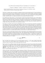
<strong>Very</strong> sharp platinum tips Martin Kupper 08309652 State of the art2.1 <strong>Electrochemical</strong> etchingThe electrochemical etching of very sharp tips is an established procedure for scanningtunneling microscopy [5]. It is possible to make tips out of different metals, butbasically the process is the same every time. A wire is dipped in an electrolyte, anda voltage is applied between the wire and a counter electrode [11]. The voltage - andwhether it is AC or DC - depends on the metal and electrolyte used and has to bedetermined <strong>by</strong> experiment. Then the oxide layer, whitch appears during the etching,has to be removed <strong>by</strong> another electrochemical step. This is usually done with a small,negative DC voltage, where the tip is the ground. It is possible to do a further stepbetween the etching and the oxide removal, called micropolishing. This is actually asecond etching with an other electrolyte or an acid, and usually a lower voltage. Thisation of cobalt and nickel 2565reduces the diameter of the head of the tip again and produces a smooth surface [2].3560 I. H. Musselman and P. E. Russell: <strong>Platinum</strong>liridium tips(a) A nickel tip etched with a (b) A Pt/Ir tip etched with CaCl 2 /H 2 O/HCl.KCl solution. [6][12]FIG. 4. SEM images of Ni tips a lower tip; b upper tip; Magnifications:FIG. 5. SEM images of the same Ptllr tip shown in Fig. 3 after micropolishing.a Radius 11000, of curvature b < SOO 300, A. Cone b half angle 800, of 8". b 3000.a 200, a 2000,Figure 2.1: Different kinds of tips.The current I flowingtips, however,duringPt peaksthewereetchingnot observedprocesssuggesting thatis shown inthe surface C layer was in excess of the escape depth ofthe PtFig. 2.Auger electron.The relative thicknesses of the surface contamination layerscan for the becut identified versus the etched inPt/Ir thetips electrochemical were determined etch-Two regimes<strong>by</strong> monitoring the intensity of the C Auger signal as a functionof sputtering time (3 keY, 25 mA emission current,ing of Me: Point 1→2 and Point 2→3. This behavior is dueto a decreased 4 charge X 10 - 5 Pa Ar). carriers For the cut concentration, tip, the C signal reached backgroundafter 45 s of sputtering, whereas the sputtering timeas a consequenceof the precipitation varied from 30 s to 3 of min the for the Me three etched complexes. Pt/lr tips. Thislarge variation in C thickness among the etched tips wasWhen the electrochemical reflected in their STM imaging etching unpredictability. starts Out Point of 20 1, hydratedchemicaletched species4Pt/Ir tips,formsapproximatelyaround20% (thosethepresumablywire, spreadingwith minimal surface C) successfully imaged sputter-deposflame.Unfortunatelyat least 30 min per tiflame temperature, iC without altering thzation. The extent oprecautions were takthe etching setup. Calevel observed for thminated from the etcreadily dissolves in wvapor pressure than<strong>by</strong> boiling and subsethe tips and to prepaing step, the contactthe thin film of etchabox under a N2 atmAuger survey speCO 2was removed frfavorably with that awerc observed for allA special method for etching tips on the is tip reverse surface etching composition. [3]. Carbon Here the was wire observed is not in all dipped offor the cut and etchein the etch solution from above, the but survey instead spectra.Anode: Mes +4Cl − from For underneath.the cut→ MeCl 2 tip, Pt peaks This4 +2e − were is carried also observeddefining the upper thickness of the carbon . contaminoutof the Pt Auger electAr + ion beam to spwith a layer of high-density electrically insulating liquid under the electrolyte. Theation layer to be between 20 and 50 A. For two of the etchedwhereas a range of 2wire is in this liquid and protudes a little in the electrolyte. This way the tips get anextremely slim shape (see Fig.2.2) [4]. However, because of the setup, doing this kindc. Image acquisitiof etching is a lot more complex then the etching from above.Two sets of nine Petching procedure wwere tested <strong>by</strong> imagspikes or streaks weusing tips from eithacquired using 80%pearance with rounhigh ranging from 1unusual features obsremaining 20% of thdesirable tip shape rface chemistry.
2 State of the art Martin Kupper 0830965rall profiles, <strong>by</strong> transmission electron microsification,of tungsten tips of decreasing conetwo-step etching. They display many minitipsat appears independent of their location alongwith water and alcohol for removregularlayer of electrolyte residue,ediately in an inert medium such asavoid oxidation or thin film depositsuntil actual use.true atomic or near-atomic sharpness,e were imaged with a high-resolutionmicroscope model Hitachi H-800NAand optimized for 0.26 nm point-to-ic profiles of tips sharpened <strong>by</strong> reprogressivelydecreasing cone anglesat low magnification. They illustratel ultrasharp minitips or spikes alongabsence of correlation between coned spike sharpness. The removal of therinsing in water and alcohol does notpness, as displayed <strong>by</strong> the very sharpic radius OS-l.0 nm and half-cone. To put in perspective the tip profilepness yielded <strong>by</strong> reverse etching andmbody in comparison with typical tipnormal etching, a clean minitip ofs (subnanometer radius) is shown inat the same magnification, on thesharp tungsten minitips of near-atomic radiushalf-cone (y-14’) unaltered <strong>by</strong> rinsing withFIG. 5. Tip of near-atomic sharpness of apex radius about 0.5-1.0 nm,formed Figure <strong>by</strong> reverse 2.2: ac Aetching reverse-etched (inside), contrasted tungsten at the same tip. magnitica- [3]tion with the outlined profile of a typically sharp apex of lOO-nm radiusformed <strong>by</strong> normal ac etching (outside).2.2 <strong>Tips</strong> for resistivity measurements.outlined profile of an optimal tip of about 100 nm radiusproduced <strong>by</strong> standard etching.In summary, a new procedure has been developed forthe production <strong>by</strong> electrochemical etching of ultrasharptungsten tips of nanometer and subnanometer apex dimensionsand its mechanism based on bubble dynamics brieflydiscussed. <strong>Tips</strong> are etched in NaOH under ac voltage intwo slow steps: In the first, a narrow cone with a fairlyblunt tip is produced, and in the second, the final sharpeningis accomplished in a modified configuration in whichthe wire is immersed pointing upward.The procedure can be extended to other metals withappropriate electrolytes.More broadly, beyond scanning probe microscopy, ultrasharptips also have applications in nanolithography,low-voltage cold-cathode field emitters, nanoelectronics,electrochemistry, field-ion and electron microscopy, andcell biology.The author is greatly indebted to Professor Noel A.Clark for use of the STM and etching setup in the CondensedMatter Laboratory and to Professor Arnold0 Majerfeldand Dr. Tamsin McCormick for use of the HitachiH-800NA transmission electron microscope in the AtomicResolution STEM Laboratory on the Boulder Campus.<strong>Sharp</strong> tips are also used for resistivity measurements in an SEM [1], where the currentdistribution of small devices is being measured. To do that, sharp tips are mountedin micromanipulators, are installed in an SEM. The tips are placed on the device, tomake electrical contact, a voltage is applied and the drop measured. In general, thereare two ways to make these measurements: first the normal resistivity measurementwith two tips, and secondly the four point resistivity measurement. For the four pointmeasurement the tips are placed in a row, a current applied between the two outer tipsand the voltage drop measured between the two inner tips (see Fig.2.3). In addition,the problem with this measurement is the tips. As mentioned in chapter 1 they bendwhen they are landed on a sample (see Fig.2.4). Because it can only be estimatedwhere the tips make contact, it is that way a relatively inaccurate measurement. Forfurther information concerning this method, visit the hompage of the Institute of SolidState Physics from the TU Graz [1].‘G. Binnig, H. Rohrer, Ch. Gerber, and E. Weibel, Phys. Rev. Lett. 49,57 (1982); 50, 120 (1983).‘G. Binnig, C. F. Quate, and Ch. Gerber, Phys. Rev. Lett. 56, 930(1986).‘J. Tersoff and D. R. Hamann, Phys. Rev. Lett. 50, 1998 (1983); Phys.Rev. B 31, 805 (1985).4T. E. Feuchtwang, P. H. Cutler, and N. M. Miskovsky, Phys. Lett. A99, 167 (1983).‘N. D. Lang, Phys. Rev. Lett. 55, 230 (1985); 56, 1164 (1986).bJ. K. Gimzewski, A. Humbert, J. G. Bednorz, and B. Reihl, Phys. Rev.Lett. 55, 951 (1985).‘Y. Kuk and P. J. Silverman, Appl. Phys. Lett. 48, 1597 (1986).‘R. Chicon, M. Ortuno, and J. Abellan, Surf. Sci. 181, 107 (1987).‘P. K. Hansma and J. Tersoff, J. Appl. Phys. 61, Rl (1987).“J. E. Demuth, U. Koehler, and R. J. Hamers, 5. Microsc. 152, 299(1988).*lY. Kuk and P. J. Silverman, Rev. Sci. Instrum. 60, 165 (1989).“L. L. Soethout, H. van Kempen, and G. F. A. van de Walle, Adv..Electron. El. Phys. 79, 155 (1990).13A. J. Mehned, J. Vat. Sci. Technol. B 9, 601 (1991).14M. Fotino, Proc. Annu. Meet. EMSA 49, 386 ( 1991).Figure 2.3: Diagram of a four point measurement [1].tt., Vol. 60, No. 23, 8 June 1992 M. Fotino 2937ded 12 Jan 2012 to 129.27.158.207. Redistribution subject to AIP license or copyright; see http://apl.aip.org/about/rights_and_permissions5