HX8347 - Adafruit
HX8347 - Adafruit HX8347 - Adafruit
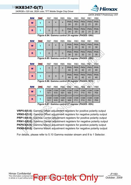
HX8347-G(T)240RGB x 320 dot, 262K color, TFT Mobile Single Chip DriverR/WWDNC1RB7RB6 RB5 RB4 RB3 RB2 RB1 RB0* * *R 1 0 0 0PKN24PKN24PKN23PKN23PKN22PKN22DATA SHEET Preliminary V01PKN21PKN21Figure 6.84: Gamma control 24 register (PAGE0 -5Ah)PKN20PKN20R/WWDNC1RB7RB6 RB5 RB4 RB3 RB2 RB1 RB0* * *PKN34PKN33PKN32PKN31PKN30R 1 0 0 0PKN34PKN33PKN32PKN31Figure 6.85: Gamma control 25 register (PAGE0 -5Bh)PKN30R/WWDNC1RB7RB6 RB5 RB4 RB3 RB2 RB1 RB0* * *PKN44PKN43PKN42PKN41PKN40R 1 0 0 0PKN44PKN43PKN42PKN41Figure 6.86: Gamma control 26 register (PAGE0 -5Ch)PKN40R/WDNCRB7RB6 RB5 RB4 RB3 RB2 RB1 RB0W1CGMN11CGMN10CGMN01CGMN00CGMP11CGMP10CGMP01CGMP00R 1CGMN11CGMN10CGMN01CGMN00CGMP11CGMP10CGMP01Figure 6.87: Gamma control 27 register (PAGE0 -5Dh)CGMP00VRP5-0[5:0]: Gamma Offset adjustment registers for positive polarity outputVRN5-0[5:0]: Gamma Offset adjustment registers for negative polarity outputPRP1-0[6:0]: Gamma Center adjustment registers for positive polarity outputPRN1-0[6:0]: Gamma Center adjustment registers for negative polarity outputPKP8-0[4:0]: Gamma Macro adjustment registers for positive polarity outputPKN8-0[4:0]: Gamma Macro adjustment registers for negative polarity outputFor details, please refer to 5.10 Gamma resister stream and 8 to 1 Selector.Himax ConfidentialFor Go-tek OnlyThis information contained herein is the exclusive property of Himax and shall not be distributed, reproduced, or disclosedin whole or in part without prior written permission of Himax.-P.160-October, 2009
HX8347-G(T)240RGB x 320 dot, 262K color, TFT Mobile Single Chip Driver6.35 TE control register (PAGE0 -60h, 84h~85h)DATA SHEET Preliminary V01R/WWDNC1RB7RB6 RB5 RB4 RB3 RB2 RB1 RB0* * *TEMODE TEON * * *R 1 0 0 0TEMODE TEON 0 0 0Figure 6.88: TE control register (PAGE0 -60h)R/WWDNC1RB7TSEL15RB6 RB5 RB4 RB3 RB2 RB1 RB0TSEL14TSEL13TSEL12TSEL11TSEL10TSEL9TSEL8R 1TSEL15TSEL14TSEL13TSEL12TSEL11TSEL10TSEL9Figure 6.89: TE output line2 register (PAGE0 -84h)TSEL8R/WWDNC1RB7TSEL7RB6 RB5 RB4 RB3 RB2 RB1 RB0TSEL6TSEL5TSEL4TSEL3TSEL2TSEL1TSEL0R 1TSEL7TSEL6TSEL5TSEL4TSEL3TSEL2TSEL1Figure 6.90: TE output line1 register (PAGE0 -85h)TEMODE: Specify the Tearing-Effect mode.When TEMODE = ‘0’: The Tearing Effect Output line (TE) consists of V-Blankinginformation only.TSEL0When TEMODE =’1’: The Tearing Effect Output Line (TE) consists of both V-Blankingand H-Blanking informationNote: During Stand by Mode with Tearing Effect Line On, Tearing Effect Output pin active lowTEON: This command is used to turn ON the Tearing Effect output signal from the TEsignal line.TSEL[15:0]: This command is used to setting TE delay line at TEMODE=”0”. WhenTSEL[15:0]=16’h0000, TE output is the same as TEMODE=”0”. WhenDecimal(TSEL[15:0])=n, TE output at n-th line starting.TSEL=0n-th linen-th lineTSEL=nHimax ConfidentialFor Go-tek OnlyThis information contained herein is the exclusive property of Himax and shall not be distributed, reproduced, or disclosedin whole or in part without prior written permission of Himax.-P.161-October, 2009
- Page 109 and 110: HX8347-G(T)240RGB x 320 dot, 262K c
- Page 111 and 112: HX8347-G(T)240RGB x 320 dot, 262K c
- Page 113 and 114: HX8347-G(T)240RGB x 320 dot, 262K c
- Page 115 and 116: HX8347-G(T)240RGB x 320 dot, 262K c
- Page 117 and 118: HX8347-G(T)240RGB x 320 dot, 262K c
- Page 119 and 120: (Hex)HX8347-G(T)240RGB x 320 dot, 2
- Page 121 and 122: HX8347-G(T)240RGB x 320 dot, 262K c
- Page 123 and 124: HX8347-G(T)240RGB x 320 dot, 262K c
- Page 125 and 126: HX8347-G(T)240RGB x 320 dot, 262K c
- Page 127 and 128: HX8347-G(T)240RGB x 320 dot, 262K c
- Page 129 and 130: HX8347-G(T)240RGB x 320 dot, 262K c
- Page 131 and 132: HX8347-G(T)240RGB x 320 dot, 262K c
- Page 133 and 134: HX8347-G(T)240RGB x 320 dot, 262K c
- Page 135 and 136: HX8347-G(T)240RGB x 320 dot, 262K c
- Page 137 and 138: HX8347-G(T)240RGB x 320 dot, 262K c
- Page 139 and 140: HX8347-G(T)240RGB x 320 dot, 262K c
- Page 141 and 142: HX8347-G(T)240RGB x 320 dot, 262K c
- Page 143 and 144: HX8347-G(T)240RGB x 320 dot, 262K c
- Page 145 and 146: HX8347-G(T)240RGB x 320 dot, 262K c
- Page 147 and 148: HX8347-G(T)240RGB x 320 dot, 262K c
- Page 149 and 150: HX8347-G(T)240RGB x 320 dot, 262K c
- Page 151 and 152: HX8347-G(T)240RGB x 320 dot, 262K c
- Page 153 and 154: HX8347-G(T)240RGB x 320 dot, 262K c
- Page 155 and 156: HX8347-G(T)240RGB x 320 dot, 262K c
- Page 157 and 158: HX8347-G(T)240RGB x 320 dot, 262K c
- Page 159: HX8347-G(T)240RGB x 320 dot, 262K c
- Page 163 and 164: HX8347-G(T)240RGB x 320 dot, 262K c
- Page 165 and 166: HX8347-G(T)240RGB x 320 dot, 262K c
- Page 167 and 168: HX8347-G(T)240RGB x 320 dot, 262K c
- Page 169 and 170: HX8347-G(T)240RGB x 320 dot, 262K c
- Page 171 and 172: HX8347-G(T)240RGB x 320 dot, 262K c
- Page 173 and 174: HX8347-G(T)240RGB x 320 dot, 262K c
- Page 175 and 176: HX8347-G(T)240RGB x 320 dot, 262K c
- Page 177 and 178: HX8347-G(T)240RGB x 320 dot, 262K c
- Page 179 and 180: HX8347-G(T)240RGB x 320 dot, 262K c
- Page 181 and 182: HX8347-G(T)240RGB x 320 dot, 262K c
- Page 183 and 184: HX8347-G(T)240RGB x 320 dot, 262K c
<strong>HX8347</strong>-G(T)240RGB x 320 dot, 262K color, TFT Mobile Single Chip DriverR/WWDNC1RB7RB6 RB5 RB4 RB3 RB2 RB1 RB0* * *R 1 0 0 0PKN24PKN24PKN23PKN23PKN22PKN22DATA SHEET Preliminary V01PKN21PKN21Figure 6.84: Gamma control 24 register (PAGE0 -5Ah)PKN20PKN20R/WWDNC1RB7RB6 RB5 RB4 RB3 RB2 RB1 RB0* * *PKN34PKN33PKN32PKN31PKN30R 1 0 0 0PKN34PKN33PKN32PKN31Figure 6.85: Gamma control 25 register (PAGE0 -5Bh)PKN30R/WWDNC1RB7RB6 RB5 RB4 RB3 RB2 RB1 RB0* * *PKN44PKN43PKN42PKN41PKN40R 1 0 0 0PKN44PKN43PKN42PKN41Figure 6.86: Gamma control 26 register (PAGE0 -5Ch)PKN40R/WDNCRB7RB6 RB5 RB4 RB3 RB2 RB1 RB0W1CGMN11CGMN10CGMN01CGMN00CGMP11CGMP10CGMP01CGMP00R 1CGMN11CGMN10CGMN01CGMN00CGMP11CGMP10CGMP01Figure 6.87: Gamma control 27 register (PAGE0 -5Dh)CGMP00VRP5-0[5:0]: Gamma Offset adjustment registers for positive polarity outputVRN5-0[5:0]: Gamma Offset adjustment registers for negative polarity outputPRP1-0[6:0]: Gamma Center adjustment registers for positive polarity outputPRN1-0[6:0]: Gamma Center adjustment registers for negative polarity outputPKP8-0[4:0]: Gamma Macro adjustment registers for positive polarity outputPKN8-0[4:0]: Gamma Macro adjustment registers for negative polarity outputFor details, please refer to 5.10 Gamma resister stream and 8 to 1 Selector.Himax ConfidentialFor Go-tek OnlyThis information contained herein is the exclusive property of Himax and shall not be distributed, reproduced, or disclosedin whole or in part without prior written permission of Himax.-P.160-October, 2009


