VLSI System Design using CADENCE - VIT University
VLSI System Design using CADENCE - VIT University
VLSI System Design using CADENCE - VIT University

Create successful ePaper yourself
Turn your PDF publications into a flip-book with our unique Google optimized e-Paper software.
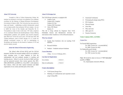
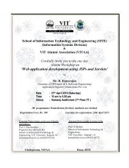
About <strong>VIT</strong> <strong>University</strong>Founded in 1984 as Vellore Engineering College, theinstitute was declared a <strong>University</strong> in recognition of its academicexcellence by the Ministry of Human Resources Development,Government of India in 2001. The <strong>University</strong> has since grown byleaps and bounds – establishing excellent infrastructure spreadover an impeccacably clean and green 360 acre campus - on wayto fulfill the vision of the founder and Chancellor Dr. G.Viswanathan to make it truly world class. <strong>VIT</strong> today comprisesof six constituent Schools and interdisciplinary Centers offeringundergraduate, graduate, post graduate and research programsupto PhD level. In the last seven years, <strong>VIT</strong> had more than 100visiting professors, some of them staying 6 to 12 weeks foroffering accelerated courses as well as participating inWorkshops and Seminars for the benefit of students of <strong>VIT</strong> andalso the industry around.About the School of Electronics EngineeringThe School offers B.Tech [ECE] and five M.Techprograms. Facilities for research leading to Ph.D. are available inmany emerging areas. A major emphasis in both theundergraduate and post graduate program is teaching andlearning process. School is actively involved in R&D activitiesand has sponsored projects from various agencies like DST,ISRO (RESPOND), and BRNS etc. It has MOU’s with industrieslike Cadence, Altera and other reputed institution and R&Dorganization of our country and other parts of the world.About <strong>VLSI</strong> design LabThe <strong>VLSI</strong> <strong>Design</strong> Laboratory is equipped with‣ Cadence ToolsCadence RTL CompilerCadence NC SimCadence SOC Encounter‣ Altera DE3 BoardQuartus- IIThis lab is being utilized by Engineers from <strong>VLSI</strong>,Embedded, Sensors and Mechatronics divisions forinnovations in their Academic as well as Research projects.Who Can Attend?‣ Faculty from Institution who are teaching <strong>VLSI</strong>DESIGN‣ Research Scholars‣ Students – Graduates and post GraduatesCourse Duration:3 Days – 21, 22, 23 February 2013.Last date for Registration:On or before : 15-02-13Date of confirmation : 17-02-13Course description:Functional VerificationPrototyping the design <strong>using</strong> FPGARTL SynthesisPhysical <strong>Design</strong>Floor PlanPlace and routeDRC and LVSParasitic ExtractionTools: Cadence EDA, ALTERACourse Fee:For Faculty/R&D organizationRs. 5000/- [course fee + accommodation]Rs. 4000/- [course fee only]For Students\Research ScholarRs. 4500/- [course fee + accommodation]Rs. 3500/- [course fee only]Note: DD should be taken in favour of “<strong>VIT</strong> <strong>University</strong>”payable at Vellore.No. of participants restricted to 30 only.<strong>VLSI</strong> <strong>System</strong> <strong>Design</strong> FlowModeling of Combinational and sequential circuits<strong>using</strong> Verilog HDL
Registration FormName : ....................................................................Department: ……………………………………………Organization :………………………………………………Experience: …………..……………………………Address for Correspondence:................................................................................................................................................................................................................................................................................................Email: ................................................................................................Phone: ...............................................................................................Accommodation Required Yes NoDemand Draft Details:Faculty /Research Scholar StudentCourse coordinators and Resource Persons:For further details contactMr.R. Sakthivel , Assistant Professor (SG)Email: rsakthivel@vit.ac.incontact No: 09994627570Mr. Ravi.S, Assistant Professor (Sr)Email: msravi@vit.ac.inContact NO: 09790155650Mr. Jagannadha Naidu K, Assistant ProfessorEmail : jagannadhanaidu.k@vit.ac.inContact No: 09943062343Registration form and DD send to:Prof.R.Sakthivel,Assistant Prof (SG)-<strong>VLSI</strong> Division,School of Electronics Engineering<strong>VIT</strong> <strong>University</strong>Vellore – 632014. TN<strong>VIT</strong>U N I V E R S I T Y(Estd. u/s 3 of UGC Act 1956)Vellore – 632014, Tamilnadu.Indiawww.vit.ac.inHands on TrainingIn<strong>VLSI</strong> SYSTEM DESIGNUSING <strong>CADENCE</strong>(RTL to GDSII)(21, 22, 23 February 2013)By<strong>VLSI</strong> DIVISIONSchool of Electronics Engineering<strong>VIT</strong> <strong>University</strong>AmountDD No.Bank: …………………………………….: …………………………………….: …………………………….……….Dated : …………………………….……….Signature: ……………………..……….(Use Photocopy of the above form, if required)<strong>VIT</strong>: A place to learn; A chance to grow
![[26th â 30th Oct 2009] - Result - VIT University](https://img.yumpu.com/48486076/1/184x260/26th-a-30th-oct-2009-result-vit-university.jpg?quality=85)