broadband millimeter-wave planar antenna array with a waveguide ...
broadband millimeter-wave planar antenna array with a waveguide ...
broadband millimeter-wave planar antenna array with a waveguide ...

Create successful ePaper yourself
Turn your PDF publications into a flip-book with our unique Google optimized e-Paper software.
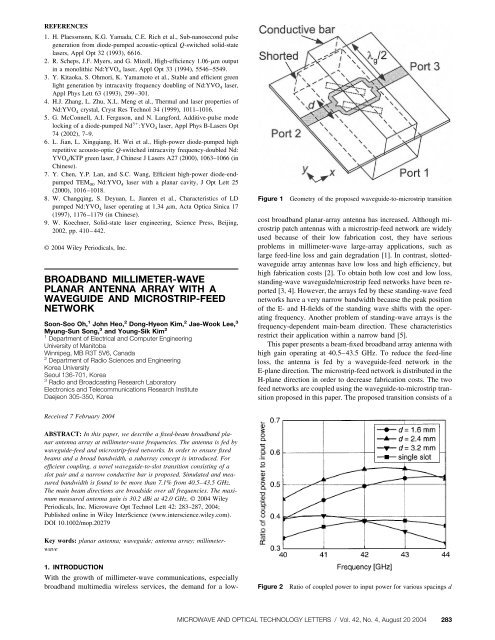
Figure 3 Ratio of coupled power to input power for a slot pair <strong>with</strong>outand <strong>with</strong> a conductive barslot pair and a conductive bar and is more efficient than a conventionaltransition. We also introduced the sub<strong>array</strong> concept, whichwidens the reflection bandwidth and fixes the main-beam directionfor variant frequencies. The whole <strong>array</strong> is divided into foursub<strong>array</strong>s that consist of eight coupling slots and 30 8 <strong>antenna</strong>elements.2. SLOT PAIR AND CONDUCTIVE BARFigure 1 shows the geometry of the proposed <strong>wave</strong>guide-to-microstriptransition. The incident <strong>wave</strong> from Port 1 is coupledthrough the slot pair and propagates toward Ports 2 and 3 wherethe microstrip feed network is attached. The slot pair consists oftwo center-inclined slots that are placed equidistant from the centerof the slot pair. The slot is 3.3 mm in length and 0.6 mm in widthand is etched on the ground plane of the substrate. The etchedground plane also serves as the upper conductor plate of the<strong>wave</strong>guide. The dielectric constant of the substrate is 2.2 and itsheight is 10 mil. Figure 2 shows the ratio of the coupled power tothe input power for various slot spacings d. The simulation hasbeen performed using Ansoft’s finite-element-method simulatorHFSS [6]. The coupled power is calculated as sum of the square ofscattering parameter, that is, S 21 2 S 31 2 . The coupling isdependent on the slot spacing d and the maximum coupling occursat d 2.4 mm. Figure 2 also shows the coupling power of a singleslot, and it is noted that the proposed slot pair <strong>with</strong> d 2.4 mmcouples more power than a single slot. This phenomenon occursbecause the slot closer to the shorted wall strongly couples theFigure 5Simulated magnitude of return loss S 11 of a sub<strong>array</strong>magnetic field at higher frequencies and the farther slot does thesame for lower frequencies.To increase coupling, we placed a thin, narrow conductiveplate, called the conductive bar, 2.0 mm above the slot pair, asshown in Figure 1. The conductive bar is 3.2 mm in width and 0.5mm in thickness. The cross bar functions as a reflector by redirectingthe radiated <strong>wave</strong> through the slot to the microstrip line.Figure 3 compares the ratio of the coupled power to the inputpower of the slot pair <strong>with</strong> and <strong>with</strong>out the conductive bar. Morepower is coupled <strong>with</strong> a conductive bar.3. SUBARRAYA sub<strong>array</strong> is configured, as shown in Figure 4. The proposed slotpairs are placed a distance of half a guided <strong>wave</strong>length, g/2,apart and their orientations are rotated alternately in order toachieve in-phase coupling. The slot pairs closest to the shortcircuitedwall of the <strong>wave</strong>guide are also positioned half a guided<strong>wave</strong>length from the shorted wall because the slot is a kind ofseries slot. In the overall <strong>array</strong> design, the microstrip-feed network<strong>with</strong> the <strong>antenna</strong> element will be attached to these slot pairs. Theincident <strong>wave</strong> is split into two feeding <strong>wave</strong>guides through aT-junction <strong>with</strong> a triangular ridge. The four slot pairs are placedalong one feeding <strong>wave</strong>guide. This scheme, called the center-feedconfiguration, is known to have a broader bandwidth than theFigure 4Geometry of a sub<strong>array</strong> (the microstrip feed network is omitted)Figure 6Geometry of the <strong>wave</strong>guide feed network284 MICROWAVE AND OPTICAL TECHNOLOGY LETTERS / Vol. 42, No. 4, August 20 2004
Figure 9 Part of the simulation model of a microstrip feed network <strong>with</strong>an <strong>antenna</strong> elementFigure 7end-feed configuration [6]. We adopted four slots along one feeding<strong>wave</strong>guide. The particular reason using four slots is that thephase difference of the coupled <strong>wave</strong> between the first and fourthslots was an endurable quantity as the simulation gave 32° at40.5 GHz and 27° at 43.5 GHz. A small phase difference meansthat the deviation of the peak of the <strong>wave</strong> is small, so that thereflection bandwidth may be broad and the beamwidth is nearlyconstant from 40.5 to 43.5 GHz. The standard WR-22 <strong>wave</strong>guidehas a dense spacing between <strong>antenna</strong> elements, which increases themutual coupling. Therefore, the width of the broad wall of the<strong>wave</strong>guide was adjusted to 4.8 mm, so that the spacing betweenslot pairs became 5.3 mm. Figure 5 illustrates the simulatedmagnitude of the return loss S 11 of the sub<strong>array</strong>. The bandwidthis nearly 3.5 GHz based on VSWR 1.5. The coupling efficiencycalculated from the power of the coupled port is 92.1% at 42.0GHz. Therefore, the sub<strong>array</strong> <strong>with</strong> the slot pair and conductive baris expected to have a broad bandwidth and high efficiency.4. FEED NETWORKModel <strong>with</strong> an additional paired slot placed between sub<strong>array</strong>s4.1. Waveguide Feed NetworkFigure 6 shows the <strong>wave</strong>guide feed network <strong>with</strong> a WR-22 inputport. The Y-junction is designed to have VSWR 1.5 at thedesired frequencies. Equal-magnitude, equal-phase <strong>wave</strong>s are fedto the sub<strong>array</strong>s. Although the <strong>wave</strong> reflected from the junctionsand sub<strong>array</strong>s is small, it becomes severe when it accumulates atthe input port. To cancel these reflections, we adjusted the<strong>wave</strong>guide length, which was d 1 d 2 d 3 d 4 , but d 3 d 1 d 2 d 4 g / 2, as shown in Figure 6. The reflected <strong>wave</strong> isoffset due to the half <strong>wave</strong>length g / 2 distance.As shown in Figure 4, the slot pair is placed half a guided<strong>wave</strong>length from the shorted end wall, so that the spacing betweenthe marginal elements of each sub<strong>array</strong> is larger than a guided<strong>wave</strong>length, because it is equal to two times half a guided <strong>wave</strong>lengthplus the wall thickness. This broad spacing results in a poorside-lobe characteristic. Therefore, a model <strong>with</strong> an additional pairof slots is proposed, as shown in Figure 7. Its parameters, such asthe microstrip-line length and slot rotation angle, are optimized tobe equal magnitude and equal phase, as compared to the neighboringslot pair.Figure 8 illustrates the complete model based on Figures 4, 6,and 7. From the results of the simulation of Figure 8 and theE-plane pattern of the <strong>antenna</strong> element, the E-plane radiationpattern is as expected [8].4.2. Microstrip Feed NetworkThe microstrip patch <strong>with</strong> a parasitic patch near the nonradiationedge described in [9] is adopted as the <strong>antenna</strong> element. Thesimulation was performed using the method of moments (MoM)tool IE3D [10]. It shows a bandwidth of 3.0 GHz (VSWR 2.1)and a well-formed radiation pattern. The microstrip feed networkis designed to have side-lobe level (SLL) of 30 dB using theDolph–Chebyshev method [8]. Figure 9 shows a partial simulationmodel consisting of a microstrip-feed network <strong>with</strong> a patch element.It is impossible to simulate the entire patch and microstripfeednetwork simultaneously, so only a 1 30 <strong>antenna</strong> <strong>array</strong> wasanalyzed and the H-plane radiation pattern was examined.5. SIMULATED AND MEASURED RESULTSFigure 10 shows a photograph of a fabricated 30 35 <strong>array</strong><strong>antenna</strong>. The substrate is attached to the base plate and secured<strong>with</strong> many metal screws. A narrow conductive bar is placedFigure 8 Completed simulation model incorporating Figs. 4, 6, and 7Figure 10Photograph of a fabricated 30 35 <strong>array</strong> <strong>antenna</strong>MICROWAVE AND OPTICAL TECHNOLOGY LETTERS / Vol. 42, No. 4, August 20 2004 285
Figure 11Simulated and measured magnitude of return loss S 11 horizontally along the centerline of the <strong>antenna</strong>, and fixed to thebase plate <strong>with</strong> screws at the both ends. The whole patch area is16.0 19.1 cm 2 . The measured return loss S 11 is compared <strong>with</strong>the simulation in Figure 8, as shown in Figure 11. Based onVSWR 2.0, both results shows a broad reflection bandwidthover 3 GHz. The simulated and measured E-plane radiation patternsare plotted in Figures 12(a) and (b), respectively. The SLLsof the simulated patterns at all frequencies are below 12 dB andthe measured SLL was also about 12 dB, except at 43.5 GHz.The SLL of about 8 dB at 43.5 GHz may have been due tofabrication tolerance. Figures 12(c) and (d) show the simulated andmeasured H-plane patterns, respectively. From the measured results,we found that the SLL was about 16 dB, while it wasdesigned to be 30 dB. The reduction from the design goal iscaused by the fabrication tolerance and mutual coupling betweenthe <strong>antenna</strong> elements and microstrip feed network. Figure 12shows that the beam widths of the E-plane pattern are almost 2.0°over all operating frequencies. This is because the sub<strong>array</strong> isconfigured in the E-plane direction. In contrast, the beam widths ofthe H-plane become broad, as the frequency is far from the centerfrequency, which is due to the center-feed configuration of theFigure 12Radiation patterns: (a) simulated and (b) measured E-plane; (c) simulated and (d) measured H-plane286 MICROWAVE AND OPTICAL TECHNOLOGY LETTERS / Vol. 42, No. 4, August 20 2004
8. W.L. Stuzman and G.A. Thiele, Antenna theory and design, Wiley,New York, 1998.9. S.S. Oh, S.H. Seo, M.K. Yoon, C.Y. Oh, E.B. Kim, and Y.S. Kim, A<strong>broadband</strong> microstrip <strong>antenna</strong> <strong>array</strong> for LMDS applications, Micro<strong>wave</strong>Optical Tech Lett 32 (2002), 35–37.10. Zeland Software, Inc., IE3D 6.0, New York, 1999.11. Y. Kimura, K. Fukazawa, J. Hirokawa, and M. Ando, Alternatingphasefed single-layer slotted <strong>wave</strong>guide <strong>array</strong>s <strong>with</strong> chokes dispensing<strong>with</strong> narrow wall contacts, IEE Proc Micro<strong>wave</strong> Antennas Propagat148 (2001), 295–301.© 2004 Wiley Periodicals, Inc.Figure 13Measured <strong>antenna</strong> gainH-plane direction. The measured <strong>antenna</strong> gain is plotted in Figure13. At the center frequency of 42.0 GHz, it has a high gain of 30.2dBi. However, degradation of about 8 dBi can be observed, ascompared to the theoretical aperture gain. This is believed to bedue to imperfect electrical contact between the ground plate of thesubstrate and the <strong>wave</strong>guide [11]. This can be overcome by usingchokes [11]. Another reason for this is the inherent conductor lossof the microstrip feed network [1].6. CONCLUSIONIn this study, a 30 35 <strong>millimeter</strong>-<strong>wave</strong> <strong>planar</strong> <strong>array</strong> <strong>antenna</strong> hasbeen designed. The <strong>array</strong> is fed by a <strong>wave</strong>guide-feed network toreduce the feed-line loss and by a microstrip-feed network toreduce the cost. A sub<strong>array</strong> was introduced <strong>with</strong> fixed beams and<strong>broadband</strong> characteristics. A novel <strong>wave</strong>guide-to-microstrip transitionwas proposed, so that strong coupling occurred over thedesired frequencies. The fabricated <strong>antenna</strong> has a reflection bandwidthof over 3.0 GHz (VSWR 2.0). SLLs below 12 dB in theE-plane are seen at all frequencies, except 43.5 GHz, while theyare below 16 dB in the H-plane. The measured <strong>antenna</strong> gain is30.2 dBi. The deterioration in pattern and gain can be improved bya perfect electrical contact or a choke. Finally, the proposed<strong>antenna</strong> <strong>array</strong> can be successfully applied to <strong>broadband</strong> <strong>millimeter</strong><strong>wave</strong>communication services.REFERENCES1. F.K. Schwering, Millimeter <strong>wave</strong> <strong>antenna</strong>s, Proc IEEE 80 (1992), 92–102.2. Y. Kimura, K. Fukazawa, J. Hirokawa, M. Ando, and N. Goto,Low-sidelobe single-layer slotted <strong>wave</strong>guide <strong>array</strong>s at 76 GHz band,IEICE Trans Commun E84-B (2001), 2377–2386.3. F.P.V.D. Wilt and J.H.M. Strijbos, A 40-GHz <strong>planar</strong> <strong>array</strong> <strong>antenna</strong>using hybrid coupling, Perspectives on radio astronomy: Tech for large<strong>antenna</strong> <strong>array</strong>s, Dig (1999), 129–134.4. F. Kolak and C. Eswarappa, A low-profile 77-GHz three-beam <strong>antenna</strong>for automotive radar, IEEE Micro<strong>wave</strong> Theory Tech Soc Int SympDig, Phoenix, AZ, (2001), 1107–1110.5. M. Hamadallah, Frequency limitations on <strong>broadband</strong> performance ofshunt slot <strong>array</strong>s, IEEE Trans Antennas Propagat 37 (1989), 817–823.6. Ansoft Corp., HFSS 8.0, PA, 2001.7. M. Müller, I.P. Theron, and D.B. Davidson, Improving the bandwidthof a slotted <strong>wave</strong>guide <strong>array</strong> by using a centre-feed configuration,IEEE Micro<strong>wave</strong> Theory Tech Soc Int Symp Dig, Los Angeles, CA,(1999), 1075–1080.A 3-mW CONCURRENT 2.4/5.2-GHzDUAL-BAND LOW-NOISE AMPLIFIERFOR WLAN APPLICATIONS IN 0.18-mCMOS TECHNOLOGYTai-Hsing Lee and Yo-Sheng LinDepartment of Electrical EngineeringNational Chi-Nan UniversityPuli, Taiwan, R.O.C.Received 5 February 2004ABSTRACT: A concurrent 2.4/5.2-GHz dual-band monolithic low-noiseamplifier implemented <strong>with</strong> a 0.18-m mixed-signal CMOS technologyis reported for the first time. This LNA only consumed 3-mW power, andachieved minimum noise figures of 3.3 and 3.26 dB and 2.4 and 5.2GHz, respectively. Input and output return losses more than 10 dB wereobtained at both 2.4 and 5.2 GHz. In addition, IIP3 of 17 and 5 dBmwere achieved at 2.4 and 5.2 GHz, respectively. No off-chip componentswere required for input and output matching. To our knowledge, thisLNA exhibits a state-of-the-art performance. Due to the careful selectionof the size of the transistors and the passive elements in our proposedmethod power matching and noise matching can be achieved simultaneouslyat the dual-band of interest. © 2004 Wiley Periodicals, Inc.Micro<strong>wave</strong> Opt Technol Lett 42: 287–292, 2004; Published online inWiley InterScience (www.interscience.wiley.com). DOI 10.1002/mop.20280Key words: concurrent; dual band; CMOS; LNA1. INTRODUCTIONWireless communication has evolved into a world of multistandards/multiservices<strong>with</strong> operating frequencies of 900 MHz/1.8GHz/1.9 GHz for GSM, 1.5 GHz for GPS, and 2.4/5.2/5.7 GHzbands for WLAN [1, 2]. Therefore, it is desirable to combine twoor more standards in one mobile unit. Conventional multibandtransceivers (the so-called nonconcurrent transceivers), which canoperate at multiple different bands, are achieved by switchingbetween multiple independent signal paths. The multiband transceiverssolution inevitably confronts some serious problems. Forexample, the cost will be increased due to additional signal path,die size, and power consumption. In addition, meticulous frequencyplanning is also an important issue. In this paper, we reporta dual-band LNA based on the concurrent dual-band receiverarchitecture [3], which is capable of simultaneous operation at twodifferent frequencies <strong>with</strong>out consuming double power or significantlyincreasing of the die size. If we elaborately choose the sizeand transconductance of the transistors and the layout of thepassive elements, the source impedance (R opt jX opt ), whichcorresponds to the minimum noise-figure condition, can be veryMICROWAVE AND OPTICAL TECHNOLOGY LETTERS / Vol. 42, No. 4, August 20 2004 287