AD546 1pA Monolithic Electrometer Operation Amplifier - ZMiTAC
AD546 1pA Monolithic Electrometer Operation Amplifier - ZMiTAC
AD546 1pA Monolithic Electrometer Operation Amplifier - ZMiTAC

Create successful ePaper yourself
Turn your PDF publications into a flip-book with our unique Google optimized e-Paper software.
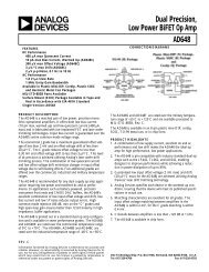
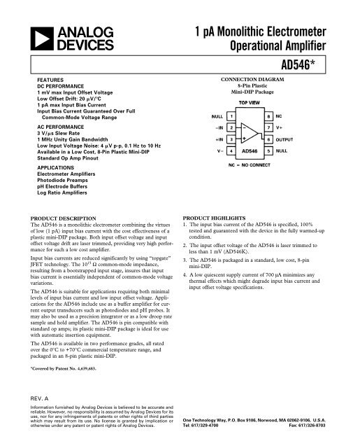
aFEATURESDC PERFORMANCE1 mV max Input Offset VoltageLow Offset Drift: 20 V/C1 pA max Input Bias CurrentInput Bias Current Guaranteed Over FullCommon-Mode Voltage RangeAC PERFORMANCE3 V/s Slew Rate1 MHz Unity Gain BandwidthLow Input Voltage Noise: 4 V p-p, 0.1 Hz to 10 HzAvailable in a Low Cost, 8-Pin Plastic Mini-DIPStandard Op Amp PinoutAPPLICATIONS<strong>Electrometer</strong> <strong>Amplifier</strong>sPhotodiode PreampspH Electrode BuffersLog Ratio <strong>Amplifier</strong>s1 pA <strong>Monolithic</strong> <strong>Electrometer</strong><strong>Operation</strong>al <strong>Amplifier</strong><strong>AD546</strong>*CONNECTION DIAGRAM8-Pin PlasticMini-DIP PackagePRODUCT DESCRIPTIONThe <strong>AD546</strong> is a monolithic electrometer combining the virtuesof low (1 pA) input bias current with the cost effectiveness of aplastic mini-DIP package. Both input offset voltage and inputoffset voltage drift are laser trimmed, providing very high performancefor such a low cost amplifier.Input bias currents are reduced significantly by using “topgate”JFET technology. The 10 15 Ω common-mode impedance,resulting from a bootstrapped input stage, insures that inputbias current is essentially independent of common-mode voltagevariations.The <strong>AD546</strong> is suitable for applications requiring both minimallevels of input bias current and low input offset voltage. Applicationsfor the <strong>AD546</strong> include use as a buffer amplifier for currentoutput transducers such as photodiodes and pH probes. Itmay also be used as a precision integrator or as a low droop ratesample and hold amplifier. The <strong>AD546</strong> is pin compatible withstandard op amps; its plastic mini-DIP package is ideal for usewith automatic insertion equipment.The <strong>AD546</strong> is available in two performance grades, all ratedover the 0°C to +70°C commercial temperature range, andpackaged in an 8-pin plastic mini-DIP.PRODUCT HIGHLIGHTS1. The input bias current of the <strong>AD546</strong> is specified, 100%tested and guaranteed with the device in the fully warmed-upcondition.2. The input offset voltage of the <strong>AD546</strong> is laser trimmed toless than 1 mV (<strong>AD546</strong>K).3. The <strong>AD546</strong> is packaged in a standard, low cost, 8-pinmini-DIP.4. A low quiescent supply current of 700 µA minimizes anythermal effects which might degrade input bias current andinput offset voltage specifications.*Covered by Patent No. 4,639,683.REV. AInformation furnished by Analog Devices is believed to be accurate andreliable. However, no responsibility is assumed by Analog Devices for itsuse, nor for any infringements of patents or other rights of third partieswhich may result from its use. No license is granted by implication orotherwise under any patent or patent rights of Analog Devices.One Technology Way, P.O. Box 9106, Norwood, MA 02062-9106, U.S.A.Tel: 617/329-4700 Fax: 617/326-8703
<strong>AD546</strong>–SPECIFICATIONS (@ +25C and 15 V dc, unless otherwise noted)<strong>AD546</strong>J <strong>AD546</strong>KModel Conditions Min Typ Max Min Typ Max UnitsINPUT BIAS CURRENT 1Either Input V CM = 0 V 0.2 1 0.2 0.5 pAEither Input V CM = ±10 V 0.1 1 0.2 0.5 pAEither Input@ T MAX V CM = 0 V 40 20 pAEither Input V CM = ±10 V 40 20 pAOffset Current V CM = 0 V 0.17 0.09 pAOffset Current@ T MAX V CM = 0 V 13 7 pAINPUT OFFSETInitial Offset 2 1 pAOffset @ T MAX 3 2 mVvs. Temperature 20 20 µV/°Cvs. Supply 100 100 µV/Vvs. Supply T MIN –T MAX 100 100 µV/VLong-Term Stability 20 20 µV/MonthINPUT VOLTAGE NOISE f = 0.1 Hz to 10 Hz 4 4 µV p-pf = 10 Hz 90 90 nV/√Hzf = 100 Hz 60 60 nV/√Hzf = 1 kHz 35 35 nV/√Hzf = 10 kHz 35 35 nV/√HzINPUT CURRENT NOISE f = 0.1 Hz to 10 Hz 1.3 1.3 fA rmsf = 1 kHz 0.4 0.4 fA/√HzINPUT IMPEDANCEDifferential V DIFF = ±1 V 10 13 1 10 13 1 ΩpFCommon Mode V CM = ±10 V 10 15 0.8 10 15 0.8 ΩpFOPEN LOOP GAINT MIN –T MAXT MIN –T MAXV O = ±10 VR LOAD = 10 kΩ 300 1000 300 1000 V/mVV O = ±10 VR LOAD = 10 kΩ 300 800 300 800 V/mVV O = ±10 VR LOAD = 2 kΩ 100 250 100 250 V/mVV O = ±10 VR LOAD = 2 kΩ 80 200 80 200 V/mVINPUT VOLTAGE RANGEDifferential 3 ±20 ±20 VCommon-Mode Voltage –10 +10 –10 +10 VCommon-Mode Rejection Ratio V CM = ±10 V 80 90 84 100 dBT MIN to T MAX 76 80 76 80 dBOUTPUT CHARACTERISTICSVoltage R LOAD = 10 kΩ –12 +12 –12 +12 VR LOAD = 2 kΩ –10 +10 –10 +10 VCurrent Short Circuit 15 20 35 15 20 35 mALoad Capacitance Stability Gain = +1 4000 4000 pF–2–REV. A
<strong>AD546</strong>–Typical Characteristics (V S = 15 V, unless otherwise noted)INPUT VOLTAGE RANGE ± V2015105+V IN–V IN00 5 10 15 20SUPPLY VOLTAGE ± VFigure 1. Input Voltage Rangevs. Supply VoltageOUTPUT VOLTAGE RANGE ± V2015105+25 o CR L = 10kΩ+V OUT–V OUT00 5 10 15 20SUPPLY VOLTAGE ± VFigure 2. Output Voltage Rangevs. Supply VoltageOUTPUT VOLTAGE SWING – Volts p-p30252015105010V S = ± 15 VOLTS100 1k 10kLOAD RESISTANCE – ΩFigure 3. Output Voltage Swingvs. Resistive Load100k8001203000QUIESCENT CURRENT – µA700600500COMMON MODE REJECTION RATIO – dB11010090804000 5 10 15 20SUPPLY VOLTAGE ± VFigure 4. Quiescent Current vs.Supply Voltage70–15 –10 0 +10 +15OPEN LOOP GAIN – V/mV1000300R L = 10kΩINPUT COMMON MODE VOLTAGE – VFigure 5. CMRR vs. InputCommon-Mode Voltage1000 5 2010 15SUPPLY VOLTAGE ± VFigure 6. Open Loop Gain vs.Supply Voltage300030300OPEN LOOP GAIN – V/mV1000300R L = 10kΩ∆ |VOS| –µV252015105INPUT BIAS CURRENT – fA250200150+25 o C100–55 –25 5 35 65 95 125TEMPERATURE – o CFigure 7. Open Loop Gain vs.Temperature00 1 2 3 4 5 6 7WARM-UP TIME – MinutesFigure 8. Change in OffsetVoltage vs. Warm-Up Time100–10 –5 0 5 10COMMON-MODE VOLTAGE – VoltsFigure 9. Input Bias Current vs.Common-Mode Voltage–4–REV. A
<strong>AD546</strong>INPUT BIAS CURRENT – fA300250200150+25 o C1000 5 10 15 20SUPPLY VOLTAGE ± VOLTSFigure 10. Input Bias Currentvs. Supply VoltageNOISE SPECTRAL DENSITY – nV/√Hz16014012010080604020101001kFREQUENCY – HzFigure 11. Input Voltage NoiseSpectral Density vs. Frequency10kINPUT NOISE VOLTAGE – µV p-p100k10k1k10010WHENEVER JOHNSON NOISE IS GREATER THANAMPLIFIER NOISE, AMPLIFIER NOISE CAN BECONSIDERED NEGLIGIBLE FOR THE APPLICATION.RESISTOR JOHNSON NOISE1 kHz BANDWIDTH10 HzBANDWIDTH1AMPLIFIER GENERATED NOISE0.1100k 1M 10M 100M 1G 10G 100GSOURCE RESISTANCE – OhmsFigure 12. Noise vs. SourceResistance10010040OPEN LOOP GAIN – dB806040200–20806040200–20PHASE MARGIN – DegreesOUTPUT VOLTAGE SWING – V3530252015105–40–4010 100 1k 10k 100k 1M 10MFREQUENCY – HzFigure 13. Open Loop FrequencyResponse0101001k 10kFREQUENCY – Hz100k1MFigure 14. Large Signal FrequencyResponseFigure 15. CMRR vs. FrequencyFigure 16. PSRR vs. FrequencyFigure 17. Output Settling Time vs.Output Swing and Error VoltageREV. A –5–
<strong>AD546</strong>Figure 18. Unity Gain FollowerFigure 19. Unity Gain FollowerLarge Signal Pulse ResponseFigure 20. Unity Gain FollowerSmall Signal Pulse ResponseFigure 21. Unity Gain InverterFigure 22. Unity Gain InverterLarge Signal Pulse ResponseFigure 23. Unity Gain InverterSmall Signal Pulse ResponseMINIMIZING INPUT CURRENTThe <strong>AD546</strong> is guaranteed to have less than 1 pA max input biascurrent at room temperature. Careful attention to how the amplifieris used will reduce input currents in actual applications.The amplifier operating temperature should be kept as low aspossible to minimize input current. Like other JFET input amplifiers,the <strong>AD546</strong>’s input current is sensitive to chip temperature,rising by a factor of 2.3 for every 10°C rise. This isillustrated in Figure 24, a plot of <strong>AD546</strong> input current versusambient temperature.On-chip power dissipation will raise chip operating temperaturecausing an increase in input bias current. Due to the <strong>AD546</strong>’slow quiescent supply current, chip temperature when the(unloaded) amplifier is operated with 15 V supplies, is less than3°C higher than ambient. The difference in input current isnegligible.However, heavy output loads can cause a significant increase inchip temperature and a corresponding increase in input current.Maintaining a minimum load resistance of 10 kΩ is recommended.Input current versus additional power dissipation dueto output drive current is plotted in Figure 25.Figure 24. <strong>AD546</strong> Input Bias Current vsAmbient TemperatureFigure 25. <strong>AD546</strong> Input Bias Current vs.Additional Power Dissipation–6–REV. A
<strong>AD546</strong>Circuit Board NotesThe <strong>AD546</strong> is designed for through hole mount into PC boards.Maintaining picoampere level resolution in that environment requiresa lot of care. Since both the printed circuit board and theamplifier’s package have a finite resistance, the voltage differencebetween the amplifier’s input pin and other pins (or traceson the PC board) will cause parasitic currents to flow into (orout of) the signal path (see Figure 26). These currents can easilyexceed the 1 pA input current level of the <strong>AD546</strong> unless specialprecautions are taken. Two successful methods for minimizingleakage are guarding the <strong>AD546</strong>’s input lines and maintainingadequate insulation resistance.The <strong>AD546</strong>’s positive input (Pin 3) is located next to the negativesupply voltage pin (Pin 4). The negative input (Pin 2) isnext to the balance adjust pin (Pin 1) which is biased at a potentialclose to the negative supply voltage. The layouts shown inFigures 27a and 27b for the inverter and follower connectionswill guard against the effects of low surface resistance of theboard. Note that the guard traces should be placed on both sidesof the board. In addition the input trace should be guarded onboth of its edges along its entire length.Figure 26. Sources of Parasitic Leakage CurrentsFigure 27a. Guarding Scheme—InverterFigure 27b. Guarding Scheme—FollowerREV. A –7–
<strong>AD546</strong>Figure 28. Input Pin to Insulating StandoffLeakage through the bulk of the circuit board will still occurwith the guarding schemes shown in Figures 27a and 27b. Standard“G10” type printed circuit board material may not havehigh enough volume resistivity to hold leakages at the subpicoamperelevel particularly under high humidity conditions.One option that eliminates all effects of board resistanceis shown in Figure 28. The <strong>AD546</strong>’s sensitive input pin (eitherPin 2 when connected as an inverter, or Pin 3 when connectedas a follower) is bent up and soldered directly to a Teflon* insulatedstandoff. Both the signal input and feedback componentleads must also be insulated from the circuit board by Teflonstandoffs or low-leakage shielded cable.Contaminants such as solder flux on the board’s surface and onthe amplifier’s package can greatly reduce the insulation resistancebetween the input pin and those traces with supply or signalvoltages. Both the package and the board must be kept cleanand dry. An effective cleaning procedure is to first swab the surfacewith high grade isopropyl alcohol, then rinse it with deionizedwater and, finally, bake it at 80°C for 1 hour. Note that ifeither polystyrene or polypropylene capacitors are used on theprinted circuit board, a baking temperature of 70°C is safer,since both of these plastic compounds begin to melt at approximately+85°C.Other guidelines include making the circuit layout as compactas possible and reducing the length of input lines. Keeping circuitboard components rigid and minimizing vibration will reducetriboelectric and piezoelectric effects. All precision highimpedance circuitry requires shielding from electrical noise andinterference. For example, a ground plane should be used underall high value (i.e., greater than 1 MΩ) feedback resistors. Insome cases, a shield placed over the resistors, or even the entireamplifier, may be needed to minimize electrical interferenceoriginating from other circuits. Referring to the equation in Figure26, this coupling can take place in either, or both, of twodifferent forms—coupling via time varying fields:Table I. Insulating Materials and CharacteristicsVolume Minimal Minimal ResistanceResistivity Triboelectric Piezoelectric to WaterMaterial 1 (–CM) Effects Effects AbsorptionTeflon* 10 17 –10 18 W W GKel-F** 10 17 –10 18 W M GSapphire 10 16 –10 18 M G GPolyethylene 10 14 –10 18 M G MPolystyrene 10 12 –10 18 W M MCeramic 10 12 –10 14 W M WGlass Epoxy 10 10 –10 17 W M WPVC 10 10 –10 15 G M GPhenolic 10 5 –10 12 W G WG–Good with Regard to Property.M–Moderate with Regard to Property.W–Weak with Regard to Property.1 Electronic Measurements, pp.15-17, Keithley Instruments, Inc., Cleveland,Ohio, 1977.*Teflon is a registered trademark of E.I. du Pont Co.**Kel-F is a registered trademark of 3M Company.OFFSET NULLINGThe <strong>AD546</strong>’s input offset voltage can be nulled by using balancePins 1 and 5, as shown in Figure 29. Nulling the input offsetvoltage in this fashion will introduce an added input offset voltagedrift component of 2.4 µV/°C per millivolt of nulled offset.dVdTC Por by injection of parasitic currents by changes in capacitancedue to mechanical vibration:dCpdT VBoth proper shielding and rigid mechanical mounting of componentshelp minimize error currents from both of these sources.Table I lists various insulators and their properties.Figure 29. Standard Offset Null CircuitThe circuit in Figure 30 can be used when the amplifier is usedas an inverter. This method introduces a small voltage in serieswith the amplifier’s positive input terminal. The amplifier’s–8–REV. A
<strong>AD546</strong>input offset voltage drift with temperature is not affected. However,variation of the power supply voltages will cause offsetshifts.Figure 32. Inverter Pulse Response with 1 MΩ Source andFeedback ResistanceFigure 30. Alternate Offset Null Circuit for InverterAC RESPONSE WITH HIGH VALUE SOURCE ANDFEEDBACK RESISTANCESource and feedback resistances greater than 100 kΩ willmagnify the effect of input capacitances (stray and inherent tothe <strong>AD546</strong>) on the ac behavior of the circuit. The effects ofcommon-mode and differential-input capacitances should betaken into account since the circuit’s bandwidth and stabilitycan be adversely affected.In a follower, the source resistance, R S , and input commonmodecapacitance, C S (including capacitance due to board andcapacitance inherent to the <strong>AD546</strong>), form a pole that limits circuitbandwidth to 1/2 π R S C S . Figure 31 shows the followerpulse response from a 1 MΩ source resistance with theamplifier’s input pin isolated from the board, only the effect ofthe <strong>AD546</strong>’s input common-mode capacitance is seen.Figure 33. Inverter Pulse Response with 1 MΩ Source andFeedback Resistance, 1 pF Feedback CapacitanceCOMMON-MODE INPUT VOLTAGE OVERLOADThe rated common-mode input voltage range of the <strong>AD546</strong> isfrom 3 V less than the positive supply voltage to 5 V greaterthan the negative supply voltage. Exceeding this range will degradethe amplifier’s CMRR. Driving the common-mode voltageabove the positive supply will cause the amplifier’s output tosaturate at the upper limit of output voltage. Recovery time istypically 2 µs after the input has been returned to within thenormal operating range. Driving the input common mode voltagewithin 1 V of the negative supply causes phase reversal ofthe output signal. In this case, normal operation is typicallyresumed within 0.5 ms of the input voltage returning withinrange.DIFFERENTIAL INPUT VOLTAGE OVERLOADA plot of the <strong>AD546</strong>’s input current versus differential inputvoltage (defined as V IN + –V IN –) appears in Figure 34. TheFigure 31. Follower Pulse Response from 1 MΩ SourceResistanceIn an inverting configuration, the differential input capacitanceforms a pole in the circuit’s loop transmission. This can createpeaking in the ac response and possible instability. A feedbackcapacitance can be used to stabilize the circuit. The inverterpulse response with R F and R S equal to 1 MΩ, and the input pinisolated from the board appears in Figure 32. Figure 33 showsthe response of the same circuit with a 1 pF feedback capacitance.Typical differential input capacitance for the <strong>AD546</strong>is 1 pF.Figure 34. Input Current vs. Differential Input VoltageREV. A –9–
<strong>AD546</strong>input current at either terminal stays below a few hundredfemtoamps until one input terminal is forced higher than 1 V to1.5 V above the other terminal. Under these conditions, theinput current limits at 30 µA.INPUT PROTECTIONThe <strong>AD546</strong> safely handles any input voltage within the supplyvoltage range. Subjecting the input terminals to voltages beyondthe power supply can destroy the device or cause shifts in inputcurrent or offset voltage if the amplifier is not protected.A protection scheme for the amplifier as an inverter is shown inFigure 35. The protection resistor, R P , is chosen to limit thecurrent through the inverting input to 1 mA for expected transient(less than 1 second) overvoltage conditions, or to 100 µAfor a continuous overload. Since R P is inside the feedback loop,and is much lower in value than the amplifier’s input resistance,it does not affect the inverter’s dc gain. However, the Johnsonnoise of the resistor will add root sum of squares to theamplifier’s input noise.than 1 pA), such as the FD333’s should be used, and should beshielded from light to keep photocurrents from being generated.Even with these precautions, the diodes will measurably increasethe input current and capacitance.In order to achieve the low input bias currents of the <strong>AD546</strong>, itis not possible to use the same on-chip protection as used inother Analog Devices op amps. This makes the <strong>AD546</strong> sensitiveto handling and precautions should be taken to minimize ESDexposure whenever possible.Figure 35. Inverter with Input Current LimitIn the corresponding version of this scheme for a follower,shown in Figure 36, R P and the capacitance at the positive inputterminal will produce a pole in the signal frequency response ata f = 1/2 π RC. Again, the Johnson noise of R P will add to theamplifier’s input voltage noise.Figure 37 is a schematic of the <strong>AD546</strong> as an inverter with an inputvoltage clamp. Bootstrapping the clamp diodes at the invertinginput minimizes the voltage across the clamps and keeps theleakage due to the diodes low. Low leakage diodes (lessFigure 36. Follower with Input Current LimitFigure 37. Input Voltage Clamp with DiodesFigure 38. Sample and Difference Circuit for Measuring<strong>Electrometer</strong> Leakage CurrentsMEASURING ELECTROMETER LEAKAGE CURRENTSThere are a number of methods used to test electrometer leakagecurrents, including current integration and direct current tovoltage conversion. Regardless of the method used, board andinterconnect cleanliness, proper choice of insulating materials(such as Teflon or Kel-F), correct guarding and shielding techniquesand care in physical layout are essential for making accurateleakage measurements.Figure 38 is a schematic of the sample and difference circuitwhich is useful for measuring the leakage currents of the <strong>AD546</strong>and other electrometer amplifiers. The circuit uses two AD549electrometer amplifiers (A and B) as current to voltage converterswith high value (10 10 Ω) sense resistors (RSa and RSb). R1and R2 provide for an overall circuit sensitivity of 10 fA/mV(10 pA full scale). C C and C F provide noise suppression andloop compensation. C C should be a low leakage polystyrene capacitor.An ultralow-leakage Kel-F test socket is used for con-–10–REV. A
<strong>AD546</strong>tacting the device under test. Rigid Teflon coaxial cable is usedto make connections to all high impedance nodes. The use ofrigid coax affords immunity to error induced by mechanical vibrationand provides an outer conductor for shielding. The entirecircuit is enclosed in a grounded metal box.The test apparatus is calibrated without a device under testpresent. A five minute stabilization period after the power isturned on is required. First, V ERR1 and V ERR2 are measured.These voltages are the errors caused by offset voltages and leakagecurrents of the current to voltage converters.V ERR1 = 10 (V OS A – I B A × RSa)V ERR2 = 10 (V OS B – I B B × RSb)Once measured, these errors are subtracted from the readingstaken with a device under test present. <strong>Amplifier</strong> B closes thefeedback loop to the device under test, in addition to providingcurrent to voltage conversion. The offset error of the device undertest appears as a common-mode signal and does not affectthe test measurement. As a result, only the leakage current ofthe device under test is measured.V A – V ERR1 = 10[RSa × I B (+)]V X – V ERR2 = 10[RSb × I B (–)]Although a series of devices can be tested after only one calibrationmeasurement, calibration should be updated periodically tocompensate for any thermal drift of the current-to-voltage convertersor changes in the ambient environment. Laboratory resultshave shown that repeatable measurements within 10 fA canbe realized when this apparatus is properly implemented. Theseresults are achieved in part by the design of the circuit, whicheliminates relays and other parasitic leakage paths in the highimpedance signal lines, and in part by the inherent cancellationof errors through the calibration and measurement procedure.PHOTODIODE INTERFACEThe <strong>AD546</strong>’s 1 pA current and low input offset voltage make ita good choice for very sensitive photodiode preamps (Figure39). The photodiode develops a signal current, I S , equal to:I S = R × Pwhere P is light power incident on the diode’s surface in wattsand R is the photodiode responsivity in amps/watt. R F convertsthe signal current to an output voltage:V OUT = R F × I SInput current, I B , will contribute an output voltage error, V E1 ,proportional to the feedback resistance:V E1 = I B × R FThe op amp’s input voltage offset will cause an error currentthrough the photodiode’s shunt resistance, R S :I = V OS /R SThe error current will result in an error voltage (V E2 ) at theamplifier’s output equal to:V E2 = (1 +R F /R S ) V OSGiven typical values of photodiode shunt resistance (on the orderof 10 9 Ω), R F /R S can be greater than one, especially if a largefeedback resistance is used. Also, R F /R S will increase with temperature,as photodiode shunt resistance typically drops by afactor of two for every 10°C rise in temperature. An op ampwith low offset voltage and low drift helps maintain accuracy.Figure 40. Photodiode Preamp DC Error SourcesPhotodiode Preamp NoiseNoise limits the signal resolution obtainable with the preamp.The output voltage noise divided by the feedback resistance isthe minimum current signal that can be detected. This minimumdetectable current divided by the responsivity of the photodioderepresents the lowest light power that can be detectedby the preamp.Noise sources associated with the photodiode, amplifier, andfeedback resistance are shown in Figure 41; Figure 42 is thevoltage spectral density versus frequency plot of each of thenoise source’s contribution to the output voltage noise (circuitparameters in Figure 40 are assumed). Each noise source’s rmscontribution to the total output voltage noise is obtained by integratingthe square of its spectral density function over frequency.The rms value of the output voltage noise is the squareroot of the sum of all contributions. Minimizing the total areaunder these curves will optimize the preamplifier’s resolution fora given bandwidth.Figure 39. Photodiode PreampDC error sources and an equivalent circuit for a small area(0.2 mm square) photodiode are indicated in Figure 40.Figure 41. Photodiode Preamp Noise SourcesREV. A –11–
<strong>AD546</strong>Figure 42. Photodiode Preamp Noise Sources’ SpectralDensity vs. FrequencyThe photodiode preamp in Figure 39 can detect a signal currentof 26 fA rms at a bandwidth of 16 Hz, which assuming a photodioderesponsivity of 0.5 A/W, translates to a 52 fW rms minimumdetectable power. The photodiode used has a high sourceresistance and low junction capacitance. C F sets the signal bandwidthwith R F and also limits the “peak” in the noise gain thatmultiplies the op amp’s input voltage noise contribution. Asingle pole filter at the amplifier’s output limits the op amp’soutput voltage noise bandwidth to 26 Hz, a frequency comparableto the signal bandwidth. This greatly improves thepreamplifier’s signal to noise ratio (in this case, by a factor ofthree).Photodiode Array ProcessorThe <strong>AD546</strong> is a cost effective preamp for multichannel applications,such as amplifying signals from photo diode arrays, as illustratedin Figure 43. An <strong>AD546</strong> preamp converts each of thediodes’ output currents to a voltage. An 8 to 1 multiplexerswitches a particular preamp output to the input of an AD138016-bit sampling ADC. The output of the ADC can be displayedor put onto a databus. Additional preamps and muxes can beadded to handle larger arrays. Layout of multichannel circuits iscritical. Refer to “PC board notes” for guidance.pH PROBE AMPLIFIERA pH probe can be modeled as a mV-level voltage source with aseries source resistance dependent upon the electrode’s compositionand configuration. The glass bulb resistance of a typicalpH electrode pair falls between 10 6 Ω and 10 9 Ω. It is, therefore,important to select an amplifier with low enough input currentssuch that the voltage drop produced by the amplifier’s inputbias current and the electrode resistance does not become anappreciable percentage of a pH unit.The circuit in Figure 44 illustrates the use of the <strong>AD546</strong> as apH probe amplifier. As with other electrometer applications, theuse of guarding, shielding, Teflon standoffs, etc., is a must inorder to capitalize on the <strong>AD546</strong>’s low input current. If an<strong>AD546</strong>J (1 pA max input current) is used, the error contributedby input current will be held below 10 mV for pH electrodesource impedances up to 10 9 Ω. Input offset voltage (which canbe trimmed) will be below 2 mV. Refer to AD549 data sheet fortemperature compensated pH probe amplifier circuit.Figure 43. Photodiode Array ProcessorFigure 44. pH Probe <strong>Amplifier</strong>OUTLINE DIMENSIONSDimensions shown in inches and (mm).Mini-DIP (N) PackagePRINTED IN U.S.A. C1291–10–7/89–12–REV. A