Power Grid Analysis in VLSI Designs - SERC
Power Grid Analysis in VLSI Designs - SERC Power Grid Analysis in VLSI Designs - SERC
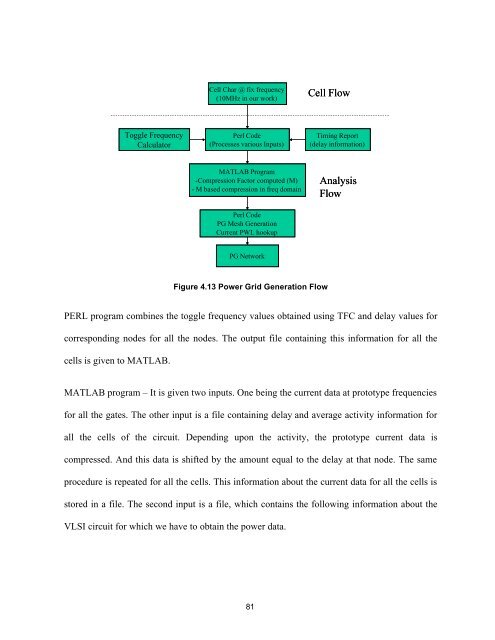
Next sections explain Power Grid Generator, Timing Information Generation and SPICEsimulation details.4.4.1 Timing Information GenerationTiming information was generated using Prime Time. Prime Time requires Verilog netlist,SDC and SPEF (Standard Parasitic Exchange Format) files as an input. We also wrote a tclscript (Prime Time supports TCL command language) to get arrival time information for allnodes of the circuit. Prime Time flow is shown in Figure 4.12 below. Sample SDC file [24][25]and SPEF used are shown in Appendix A and B.SDC FileVerilogNetlistSPEFPrime TimeArrival TimeComputationTiming ReportFigure 4.12 Prime Time flow for arrival time computation4.4.2 Power Grid GeneratorThe Power Grid Generator flow is expanded further below in Figure 4.13.80
Cell Char @ fix frequency(10MHz in our work)Cell FlowToggle FrequencyCalculatorPerl Code(Processes various Inputs)Timing Report(delay information)MATLAB Program-Compression Factor computed (M)- M based compression in freq domainPerl CodePG Mesh GenerationCurrent PWL hookupAnalysisFlowPG NetworkFigure 4.13 Power Grid Generation FlowPERL program combines the toggle frequency values obtained using TFC and delay values forcorresponding nodes for all the nodes. The output file containing this information for all thecells is given to MATLAB.MATLAB program – It is given two inputs. One being the current data at prototype frequenciesfor all the gates. The other input is a file containing delay and average activity information forall the cells of the circuit. Depending upon the activity, the prototype current data iscompressed. And this data is shifted by the amount equal to the delay at that node. The sameprocedure is repeated for all the cells. This information about the current data for all the cells isstored in a file. The second input is a file, which contains the following information about theVLSI circuit for which we have to obtain the power data.81
- Page 29 and 30: For large T, D(x) becomes time inva
- Page 31 and 32: done hierarchically or there is reu
- Page 33 and 34: A Sample SDC file with above comman
- Page 35 and 36: Some of the care needs to be taken
- Page 37 and 38: Figure 2.5 Timing Arcs in extracted
- Page 39 and 40: 3 Power Estimation3.1 OverviewAccur
- Page 41 and 42: In this work, above power component
- Page 43 and 44: on the required accuracy, different
- Page 45 and 46: Based on power sensitivity and tool
- Page 47 and 48: with SPICE. Power Mill is dynamic s
- Page 49 and 50: DREPGENDREPFILE+ DATAGENFUNCTDLRAND
- Page 51 and 52: 3.4.3 Interconnect setupAll the cir
- Page 53 and 54: DesignNameIN OUT Flops Boolean(gate
- Page 55 and 56: Design TFC + Power Compiler Runtime
- Page 57 and 58: Design Name CLK Power Total Power %
- Page 59 and 60: DesignNamePowerCompilerProposedAppr
- Page 61 and 62: We can approximate the average powe
- Page 63 and 64: 4 Power Supply Noise Analysis4.1 Ov
- Page 65 and 66: to be absolutely in complete alignm
- Page 67 and 68: In this work, we have maintained te
- Page 69 and 70: Figure 4.6 Load vs. peak power for
- Page 71 and 72: 3. The temporal correlation between
- Page 73 and 74: Each such armRepresents resistance
- Page 75 and 76: Characterized data was transformed
- Page 77 and 78: Do timing analysis and based on inp
- Page 79: of any node. Alternatively frequenc
- Page 83 and 84: We executed the flow as explained i
- Page 85 and 86: Circuit%Drop inaverage activity%Dro
- Page 87: 4.6 SummaryWe proposed novel PG net
- Page 90 and 91: network but causing huge dynamic IR
- Page 92 and 93: Power SwitchFigure 5.2 Layout of 1M
- Page 94 and 95: power network start getting charged
- Page 96 and 97: Note that the 1 stcharacterization
- Page 98 and 99: • Maximum current surge that will
- Page 100 and 101: gates in the virtual network or mor
- Page 102 and 103: Vdesired (mV)Actual#SwitchesSwitche
- Page 104 and 105: 5.4 SummaryThere are various techni
- Page 106 and 107: 5. Power Up analysis for MTCMOS bas
- Page 108 and 109: 108
- Page 110 and 111: 21. F.N. Najm, R.Burch, P. Yang, an
- Page 112 and 113: 62. H. Mehta, R.M.Owens, M.J.Irwin,
- Page 114 and 115: 114
- Page 116 and 117: Appendix B Sample SPEF Format*SPEF
- Page 118 and 119: Appendix C Power Waveforms Analysis
- Page 120 and 121: Appendix E Waveform transformation
Cell Char @ fix frequency(10MHz <strong>in</strong> our work)Cell FlowToggle FrequencyCalculatorPerl Code(Processes various Inputs)Tim<strong>in</strong>g Report(delay <strong>in</strong>formation)MATLAB Program-Compression Factor computed (M)- M based compression <strong>in</strong> freq doma<strong>in</strong>Perl CodePG Mesh GenerationCurrent PWL hookup<strong>Analysis</strong>FlowPG NetworkFigure 4.13 <strong>Power</strong> <strong>Grid</strong> Generation FlowPERL program comb<strong>in</strong>es the toggle frequency values obta<strong>in</strong>ed us<strong>in</strong>g TFC and delay values forcorrespond<strong>in</strong>g nodes for all the nodes. The output file conta<strong>in</strong><strong>in</strong>g this <strong>in</strong>formation for all thecells is given to MATLAB.MATLAB program – It is given two <strong>in</strong>puts. One be<strong>in</strong>g the current data at prototype frequenciesfor all the gates. The other <strong>in</strong>put is a file conta<strong>in</strong><strong>in</strong>g delay and average activity <strong>in</strong>formation forall the cells of the circuit. Depend<strong>in</strong>g upon the activity, the prototype current data iscompressed. And this data is shifted by the amount equal to the delay at that node. The sameprocedure is repeated for all the cells. This <strong>in</strong>formation about the current data for all the cells isstored <strong>in</strong> a file. The second <strong>in</strong>put is a file, which conta<strong>in</strong>s the follow<strong>in</strong>g <strong>in</strong>formation about the<strong>VLSI</strong> circuit for which we have to obta<strong>in</strong> the power data.81


