Power Grid Analysis in VLSI Designs - SERC
Power Grid Analysis in VLSI Designs - SERC
Power Grid Analysis in VLSI Designs - SERC

Create successful ePaper yourself
Turn your PDF publications into a flip-book with our unique Google optimized e-Paper software.
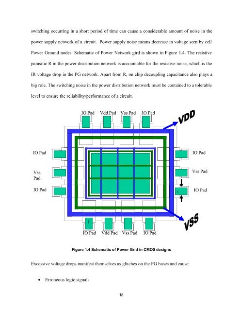
switch<strong>in</strong>g occurr<strong>in</strong>g <strong>in</strong> a short period of time can cause a considerable amount of noise <strong>in</strong> thepower supply network of a circuit. <strong>Power</strong> supply noise means decrease <strong>in</strong> voltage seen by cell<strong>Power</strong> Ground nodes. Schematic of <strong>Power</strong> Network gird is shown <strong>in</strong> Figure 1.4. The resistiveparasitic R <strong>in</strong> the power distribution network is accountable for the resistive noise, which is theIR voltage drop <strong>in</strong> the PG network. Apart from R, on chip decoupl<strong>in</strong>g capacitance also plays abig role. The switch<strong>in</strong>g noise <strong>in</strong> the power distribution network must be conta<strong>in</strong>ed to a tolerablelevel to ensure the reliability/performance of a circuit.IO PadVdd Pad Vss Pad IO PadIO PadIO PadVssPadIO Pad5Vss PadIO Pad1IO PadVdd Pad Vss Pad IO PadFigure 1.4 Schematic of <strong>Power</strong> <strong>Grid</strong> <strong>in</strong> CMOS designsExcessive voltage drops manifest themselves as glitches on the PG buses and cause:• Erroneous logic signals18