- Page 1:
Power Grid Analysis in VLSI Designs
- Page 6 and 7:
4.4.1 Timing Information Generation
- Page 8 and 9:
Figure 3 1GHz, Peak: 838.2 uW......
- Page 11 and 12:
AbstractPower has become an importa
- Page 13 and 14:
1 Introduction1.1 MotivationVLSI in
- Page 15 and 16:
Further, Figure 1.3 shows that ther
- Page 17 and 18:
proposed in a few papers. In this t
- Page 19 and 20:
• Degradation in switching speeds
- Page 21 and 22:
Second, today’s design has huge P
- Page 23 and 24:
Figure 1.6 Total power break up int
- Page 25 and 26:
CMOSDieAcronym for Complimentary Me
- Page 27 and 28:
2 Toggle Activity Estimation2.1 Ove
- Page 29 and 30:
For large T, D(x) becomes time inva
- Page 31 and 32:
done hierarchically or there is reu
- Page 33 and 34:
A Sample SDC file with above comman
- Page 35 and 36:
Some of the care needs to be taken
- Page 37 and 38:
Figure 2.5 Timing Arcs in extracted
- Page 39 and 40:
3 Power Estimation3.1 OverviewAccur
- Page 41 and 42:
In this work, above power component
- Page 43 and 44:
on the required accuracy, different
- Page 45 and 46:
Based on power sensitivity and tool
- Page 47 and 48:
with SPICE. Power Mill is dynamic s
- Page 49 and 50:
DREPGENDREPFILE+ DATAGENFUNCTDLRAND
- Page 51 and 52:
3.4.3 Interconnect setupAll the cir
- Page 53 and 54:
DesignNameIN OUT Flops Boolean(gate
- Page 55 and 56:
Design TFC + Power Compiler Runtime
- Page 57 and 58:
Design Name CLK Power Total Power %
- Page 59 and 60:
DesignNamePowerCompilerProposedAppr
- Page 61 and 62:
We can approximate the average powe
- Page 63 and 64:
4 Power Supply Noise Analysis4.1 Ov
- Page 65 and 66: to be absolutely in complete alignm
- Page 67 and 68: In this work, we have maintained te
- Page 69 and 70: Figure 4.6 Load vs. peak power for
- Page 71 and 72: 3. The temporal correlation between
- Page 73 and 74: Each such armRepresents resistance
- Page 75 and 76: Characterized data was transformed
- Page 77 and 78: Do timing analysis and based on inp
- Page 79 and 80: of any node. Alternatively frequenc
- Page 81 and 82: Cell Char @ fix frequency(10MHz in
- Page 83 and 84: We executed the flow as explained i
- Page 85 and 86: Circuit%Drop inaverage activity%Dro
- Page 87: 4.6 SummaryWe proposed novel PG net
- Page 90 and 91: network but causing huge dynamic IR
- Page 92 and 93: Power SwitchFigure 5.2 Layout of 1M
- Page 94 and 95: power network start getting charged
- Page 96 and 97: Note that the 1 stcharacterization
- Page 98 and 99: • Maximum current surge that will
- Page 100 and 101: gates in the virtual network or mor
- Page 102 and 103: Vdesired (mV)Actual#SwitchesSwitche
- Page 104 and 105: 5.4 SummaryThere are various techni
- Page 106 and 107: 5. Power Up analysis for MTCMOS bas
- Page 108 and 109: 108
- Page 110 and 111: 21. F.N. Najm, R.Burch, P. Yang, an
- Page 112 and 113: 62. H. Mehta, R.M.Owens, M.J.Irwin,
- Page 114 and 115: 114
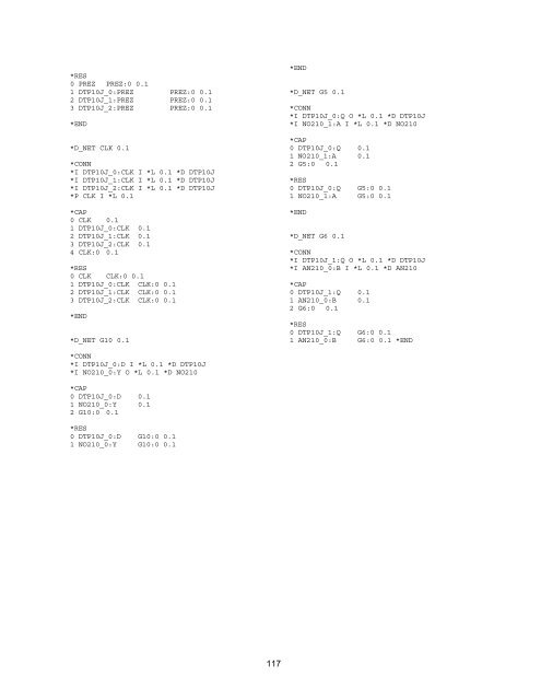
- Page 118 and 119: Appendix C Power Waveforms Analysis
- Page 120 and 121: Appendix E Waveform transformation