

Cyclone V SoC FPGA Development Board Reference Manual - Altera
Cyclone V SoC FPGA Development Board Reference Manual - Altera
Cyclone V SoC FPGA Development Board Reference Manual - Altera

Create successful ePaper yourself
Turn your PDF publications into a flip-book with our unique Google optimized e-Paper software.
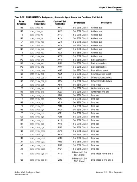
2–40 Chapter 2: <strong>Board</strong> ComponentsMemoryTable 2–32. DDR3 SDRAM Pin Assignments, Schematic Signal Names, and Functions (Part 3 of 4)<strong>Board</strong><strong>Reference</strong>SchematicSignal Name<strong>Cyclone</strong> V <strong>SoC</strong>Pin NumberR8 DDR3_<strong>FPGA</strong>_A6 AK12 1.5-V SSTL Class I Address busR2 DDR3_<strong>FPGA</strong>_A7 AK13 1.5-V SSTL Class I Address busT8 DDR3_<strong>FPGA</strong>_A8 AH13 1.5-V SSTL Class I Address busR3 DDR3_<strong>FPGA</strong>_A9 AH14 1.5-V SSTL Class I Address busL7 DDR3_<strong>FPGA</strong>_A10 AJ9 1.5-V SSTL Class I Address busR7 DDR3_<strong>FPGA</strong>_A11 AK9 1.5-V SSTL Class I Address busN7 DDR3_<strong>FPGA</strong>_A12 AK7 1.5-V SSTL Class I Address busT3 DDR3_<strong>FPGA</strong>_A13 AK8 1.5-V SSTL Class I Address busT7 DDR3_<strong>FPGA</strong>_A14 AG12 1.5-V SSTL Class I Address busM2 DDR3_<strong>FPGA</strong>_BA0 AH10 1.5-V SSTL Class I Bank address busN8 DDR3_<strong>FPGA</strong>_BA1 AJ11 1.5-V SSTL Class I Bank address busM3 DDR3_<strong>FPGA</strong>_BA2 AK11 1.5-V SSTL Class I Bank address busK3 DDR3_<strong>FPGA</strong>_CASN AH7 1.5-V SSTL Class I Row address selectK9 DDR3_<strong>FPGA</strong>_CKE AJ21 1.5-V SSTL Class I Column address selectJ7 DDR3_<strong>FPGA</strong>_CLK_P AA15 1.5-V SSTL Class I Differential output clockK7 DDR3_<strong>FPGA</strong>_CLK_N AA14 1.5-V SSTL Class I Differential output clockL2 DDR3_<strong>FPGA</strong>_CSN AB15 1.5-V SSTL Class I Chip selectE7 DDR3_<strong>FPGA</strong>_DM0 AH17 1.5-V SSTL Class I Write mask byte laneD3 DDR3_<strong>FPGA</strong>_DM1 AG23 1.5-V SSTL Class I Write mask byte laneE3 DDR3_<strong>FPGA</strong>_DQ0 AF18 1.5-V SSTL Class I Data busF2 DDR3_<strong>FPGA</strong>_DQ1 AE17 1.5-V SSTL Class I Data busH8 DDR3_<strong>FPGA</strong>_DQ2 AG16 1.5-V SSTL Class I Data busF8 DDR3_<strong>FPGA</strong>_DQ3 AF16 1.5-V SSTL Class I Data busH3 DDR3_<strong>FPGA</strong>_DQ4 AH20 1.5-V SSTL Class I Data busF7 DDR3_<strong>FPGA</strong>_DQ5 AG21 1.5-V SSTL Class I Data busG2 DDR3_<strong>FPGA</strong>_DQ6 AJ16 1.5-V SSTL Class I Data busH7 DDR3_<strong>FPGA</strong>_DQ7 AH18 1.5-V SSTL Class I Data busD7 DDR3_<strong>FPGA</strong>_DQ8 AK18 1.5-V SSTL Class I Data busC8 DDR3_<strong>FPGA</strong>_DQ9 AJ17 1.5-V SSTL Class I Data busC3 DDR3_<strong>FPGA</strong>_DQ10 AG18 1.5-V SSTL Class I Data busC2 DDR3_<strong>FPGA</strong>_DQ11 AK19 1.5-V SSTL Class I Data busB8 DDR3_<strong>FPGA</strong>_DQ12 AG20 1.5-V SSTL Class I Data busA7 DDR3_<strong>FPGA</strong>_DQ13 AF19 1.5-V SSTL Class I Data busA2 DDR3_<strong>FPGA</strong>_DQ14 AJ20 1.5-V SSTL Class I Data busA3 DDR3_<strong>FPGA</strong>_DQ15 AH24 1.5-V SSTL Class I Data busF3 DDR3_<strong>FPGA</strong>_DQS_P0 V16G3 DDR3_<strong>FPGA</strong>_DQS_N0 W16I/O StandardDifferential 1.5-VSSTL Class IDifferential 1.5-VSSTL Class IDescriptionData strobe P byte lane 0Data strobe N byte lane 0<strong>Cyclone</strong> V <strong>SoC</strong> <strong>Development</strong> <strong>Board</strong> November 2013 <strong>Altera</strong> Corporation<strong>Reference</strong> <strong>Manual</strong>


