Cyclone V SoC FPGA Development Board Reference Manual - Altera
Cyclone V SoC FPGA Development Board Reference Manual - Altera
Cyclone V SoC FPGA Development Board Reference Manual - Altera
You also want an ePaper? Increase the reach of your titles
YUMPU automatically turns print PDFs into web optimized ePapers that Google loves.
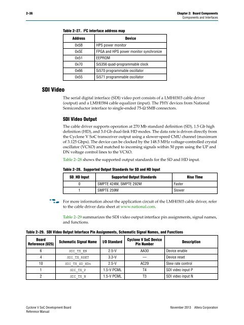
2–36 Chapter 2: <strong>Board</strong> ComponentsComponents and InterfacesTable 2–27. I 2 C interface address mapAddress0x5B0x5E0x510x700x660x55DeviceHPS power monitor<strong>FPGA</strong> and HPS power monitor synchronizeEEPROMSi5356 quad-programmable clockSi570 programmable oscillatorSi571 programmable oscillatorSDI VideoThe serial digital interface (SDI) video port consists of a LMH0303 cable driver(output) and a LMH0384 cable equalizer (input). The PHY devices from NationalSemiconductor interface to single-ended 75-Ω SMB connectors.SDI Video OutputThe cable driver supports operation at 270 Mb standard definition (SD), 1.5 Gb highdefinition (HD), and 3.0 Gb dual-link HD modes. The data rate is driven directly fromthe <strong>Cyclone</strong> V <strong>SoC</strong> transceiver output using a slower-speed CMU channel (maximumof 3.125 Gbps). The device can be clocked by the 148.5 MHz voltage-controlled crystaloscillator (VCXO) and matched to incoming signals within 50 ppm using the UP andDN voltage control lines to the VCXO.Table 2–28 shows the supported output standards for the SD and HD input.Table 2–28. Supported Output Standards for SD and HD InputSD_HD Input Supported Output Standards Rise TIme0 SMPTE 424M, SMPTE 292M Faster1 SMPTE 259M SlowerfFor more information about the application circuit of the LMH0303 cable driver, referto the cable driver data sheet at www.national.com.Table 2–29 summarizes the SDI video output interface pin assignments, signal names,and functions.Table 2–29. SDI Video Output Interface Pin Assignments, Schematic Signal Names, and Functions<strong>Board</strong><strong>Reference</strong> (U25)Schematic Signal NameI/O Standard<strong>Cyclone</strong> V <strong>SoC</strong> DevicePin NumberDescription6 SDI_TX_EN 2.5-V AA30 Device enable4 SDI_TX_RSET 3.3-V — Device reset10 SDI_TX_SD_HDn 2.5-V AC29 Slew rate control1 SDI_TX_P 1.5-V PCML T4 SDI video input P2 SDI_TX_N 1.5-V PCML T3 SDI video input N<strong>Cyclone</strong> V <strong>SoC</strong> <strong>Development</strong> <strong>Board</strong> November 2013 <strong>Altera</strong> Corporation<strong>Reference</strong> <strong>Manual</strong>


