Root-Cause Failure Analysis of Electronics - SMTA
Root-Cause Failure Analysis of Electronics - SMTA
Root-Cause Failure Analysis of Electronics - SMTA
- No tags were found...

Create successful ePaper yourself
Turn your PDF publications into a flip-book with our unique Google optimized e-Paper software.
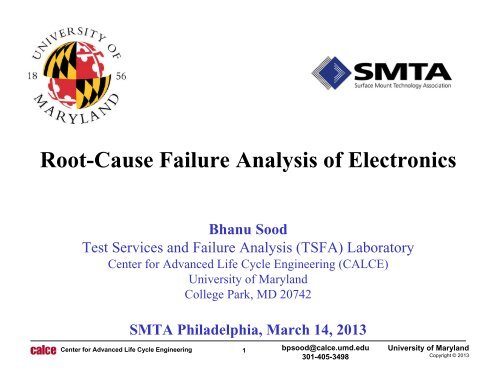
<strong>Root</strong>-<strong>Cause</strong> <strong>Failure</strong> <strong>Analysis</strong> <strong>of</strong> <strong>Electronics</strong>Bhanu SoodTest Services and <strong>Failure</strong> <strong>Analysis</strong> (TSFA) LaboratoryCenter for Advanced Life Cycle Engineering (CALCE)University <strong>of</strong> MarylandCollege Park, MD 20742Center for Advanced Life Cycle Engineering<strong>SMTA</strong> Philadelphia, March 14, 20131bpsood@calce.umd.edu301-405-3498University <strong>of</strong> MarylandCopyright © 2013
Content DisclaimerThe information contained in this packet is designed to be accurate and authoritative in regardsto the subject matter covered. However, it is provided with the understanding that the provider isnot engaged in rendering legal, accounting, engineering, or other pr<strong>of</strong>essional services. It isintended to be used for educational purposes only. Individual presenters, their respectiveorganizations and Center for Advanced Life Cycle Engineering (CALCE) disclaim anyresponsibility or liability for this material and are not responsible for the use <strong>of</strong> this informationoutside <strong>of</strong> its educational purpose.Copyright NoticeThe information contained within this packet has been compiled by theUniversity <strong>of</strong> Maryland, CALCEReplication rights <strong>of</strong> all information is retained by individual presenters, their respectiveorganizations and CALCE.Copyright © 2013 CALCE and the University <strong>of</strong> Maryland. All rights reserved.
What are the Biggest Headaches?• CALCE Laboratory Servicesreviewed 150 root-causeanalyses <strong>of</strong> failures duringqualification or at a customersite– Representative <strong>of</strong> over 80different companies.• These failures werecategorized by failure site– PCB and capacitor issuesaccounted for over 50% <strong>of</strong>these failures.Center for Advanced Life Cycle EngineeringInterconnects/Solder Joints 13%2PEM 21%bpsood@calce.umd.edu301-405-3498Other Sites 7%Connectors 3%Capacitors 30%Printed Board 26%University <strong>of</strong> MarylandCopyright © 2013Where there are <strong>Failure</strong>s… There Are Costs . . .• Costs to the Manufacturero Time-to-market can increaseo Warranty costs can increaseo Market share can decrease. <strong>Failure</strong>s can stain thereputation <strong>of</strong> a company, and deter new customers.o Claims for damages caused by product failure can increase• Costs to the Customero Personal injuryo Loss <strong>of</strong> mission, service or capacityo Cost <strong>of</strong> repair or replacemento Indirect costs, such as increase in insurance, damage toreputation, loss <strong>of</strong> market shareCenter for Advanced Life Cycle Engineering3bpsood@calce.umd.edu301-405-3498University <strong>of</strong> MarylandCopyright © 2013Type <strong>of</strong> BusinessWhat is the Cost <strong>of</strong> <strong>Failure</strong>?*Retail Brokerages $6,450,000Credit Card Sales Authorization $2,600,000Home Shopping Channels $113,750Catalog Sales Centers $90,000Airline Reservation Centers $89,500Cellular Service Activations $41,000Package Shipping Services $28,250Online Network Connect Fees $22,250ATM Service Fees $14,500Supermarkets $10,000Lost Revenue per HourOutline• Definitions• <strong>Root</strong> cause failure analysis– RCA Steps• Case Studies• Closing remarks* - 1999 dollarsCenter for Advanced Life Cycle Engineering4bpsood@calce.umd.edu301-405-3498University <strong>of</strong> MarylandCopyright © 2013Center for Advanced Life Cycle Engineering5bpsood@calce.umd.edu301-405-3498University <strong>of</strong> MarylandCopyright © 2013
<strong>Failure</strong> Definitions<strong>Failure</strong> <strong>Analysis</strong><strong>Failure</strong><strong>Failure</strong> Mode<strong>Failure</strong> Site<strong>Failure</strong> MechanismA product no longer performs the function for which itwas intendedThe effect by which a failure is observed.The location <strong>of</strong> the failure.The physical, chemical, thermodynamic or other processthat results in failure.<strong>Failure</strong> ModelLoadQuantitative relationship between lifetime or probability<strong>of</strong> failure and loadsApplication/environmental condition needed (electrical,thermal, mechanical, chemical...) to precipitate a failuremechanism.Center for Advanced Life Cycle Engineering6bpsood@calce.umd.edu301-405-3498University <strong>of</strong> MarylandCopyright © 2013Center for Advanced Life Cycle Engineering7bpsood@calce.umd.edu301-405-3498University <strong>of</strong> MarylandCopyright © 2013Classification <strong>of</strong> <strong>Failure</strong>s<strong>Failure</strong> Mechanism Identification• It is helpful to distinguish between two key classes <strong>of</strong>failure mechanism:– overstress: use conditions exceed strength <strong>of</strong> materials; <strong>of</strong>tensudden and catastrophic– wearout: accumulation <strong>of</strong> damage with extended usage or repeatedstress• It is also helpful to recognize early life failures:– infant mortality: failures occurring early in expected life; should beeliminated through process control, part selection andmanagement, and quality improvement proceduresOverstress MechanismsMechanicalThermalElectricalRadiationChemicalYield, Fracture,Interfacial de-adhesionGlass transition (T g)Phase transitionDielectric breakdown,Electrical overstress,Electrostatic discharge,Second breakdownSingle event upsetContaminationWearout MechanismsMechanicalThermalElectricalRadiationChemicalFatigue,Creep, WearStress driven diffusionvoiding (SDDV)TDDB, Electromigration,Surface chargespreading, Hot electrons,CAF, Slow trappingRadiation embrittlement,Charge trapping inoxidesCorrosion,Dendrite growth,Depolymerization,Intermetallic GrowthCenter for Advanced Life Cycle Engineering8bpsood@calce.umd.edu301-405-3498University <strong>of</strong> MarylandCopyright © 2013Center for Advanced Life Cycle Engineering9bpsood@calce.umd.edu301-405-3498University <strong>of</strong> MarylandCopyright © 2013
What <strong>Cause</strong>s Products to Fail?• Generally, failures do not “just happen.”• <strong>Failure</strong>s may arise during any <strong>of</strong> the following stages <strong>of</strong> aproduct’s life cycle:What is <strong>Root</strong> <strong>Cause</strong> <strong>Analysis</strong>?<strong>Root</strong> <strong>Cause</strong> analysis has four major objectives:• Verify that a failure occurred;• Determine the symptom or the apparent way a part has failed(the mode);• Determine the mechanism and root cause <strong>of</strong> the failure;• Recommend corrective and preventative action.The damage (failure mode) may not be detected until a laterphase <strong>of</strong> the life cycle.Center for Advanced Life Cycle Engineering10bpsood@calce.umd.edu301-405-3498University <strong>of</strong> MarylandCopyright © 2013While generally synonymous, “<strong>Failure</strong> analysis” iscommonly understood to include all <strong>of</strong> this exceptdetermination <strong>of</strong> root cause.Center for Advanced Life Cycle Engineering11bpsood@calce.umd.edu301-405-3498University <strong>of</strong> MarylandCopyright © 2013What is a <strong>Root</strong> <strong>Cause</strong>The root cause is the most basic causal factor or factorsthat, if corrected or removed, will prevent therecurrence <strong>of</strong> the situation.*The purpose <strong>of</strong> determining the root cause (s) is to fix theproblem at its most basic source so it doesn’t occur again,even in other products, as opposed to merely fixing afailure symptom. Identifying root causes is the key topreventing similar occurrences in the future.<strong>Root</strong> <strong>Cause</strong> <strong>Analysis</strong> isDifferent from Troubleshooting• Troubleshooting is generally employed toeliminate a symptom in a given product, or toidentify a failed component in order to effect arepair.• <strong>Root</strong> cause analysis is dedicated to finding thefundamental reason why the problem occurred inthe first place, to prevent future failures.* ABS Group, Inc., <strong>Root</strong> <strong>Cause</strong> <strong>Analysis</strong> Handbook, A Guide to EffectiveIncident Investigation, ABS Group, Inc., Risk & Reliability Division,Rockville, MD, 1999.Center for Advanced Life Cycle Engineering12bpsood@calce.umd.edu301-405-3498University <strong>of</strong> MarylandCopyright © 2013Center for Advanced Life Cycle Engineering13bpsood@calce.umd.edu301-405-3498University <strong>of</strong> MarylandCopyright © 2013
From Symptoms to <strong>Root</strong> <strong>Cause</strong>s• Symptoms are manifestations <strong>of</strong> a problem; signs indicatingthat a failure exists.– Example: a symptom <strong>of</strong> printed circuit board failure could be themeasurement <strong>of</strong> open circuits after fabrication.• An apparent cause (or immediately visible cause)is the superficial reason for the failure.– Example: the apparent cause <strong>of</strong> open circuits could be that traceshave discontinuities which result in open circuits.• <strong>Root</strong> <strong>Cause</strong> is the most basic casual factor(s).– Example: the root cause could arise during the manufacturingprocess if the circuit boards are stacked improperly, resulting inscratches to circuit traces. Another possible root cause could be thepresence <strong>of</strong> contaminants during the copper trace etching process,which resulted in discontinuities in the traces.<strong>Root</strong> <strong>Cause</strong> <strong>Analysis</strong>• <strong>Root</strong> cause analysis is a methodology designed to help:1) Describe WHAT happened during a particular occurrence,2) Determine HOW it happened, and3) Understand WHY it happened.• Only when one is able to determine WHY an event or failureoccurred, will one be able to determine corrective measures, andover time, the root causes identified can be used to target majoropportunities for improvement.• Uncovering ROOT CAUSE may require 7 iterations <strong>of</strong> “Why?”Center for Advanced Life Cycle Engineering14bpsood@calce.umd.edu301-405-3498University <strong>of</strong> MarylandCopyright © 2013Center for Advanced Life Cycle Engineering15bpsood@calce.umd.edu301-405-3498University <strong>of</strong> MarylandCopyright © 2013Preplanning: Establish <strong>Root</strong> <strong>Cause</strong> Culture with Management Support and Responsibilities Policy/procedures for notification Trained investigation team Hypothesization Tools Classification system <strong>Analysis</strong> procedures Risk <strong>Analysis</strong>Alert / Notification : Begin Investigation Secure evidence (data collection) Assess immediate cause(s) Interview witnessesHypothesize causes using tools such as Ishikawa (fishbone) diagram, and failure modes, mechanisms,and effects analysis (FMMEA)Identify <strong>Root</strong> <strong>Cause</strong> (s)Identify Restart CriteriaDevelop Corrective Actions<strong>Root</strong> <strong>Cause</strong> <strong>Analysis</strong> ProcessTheIncident!Analyze and Interpret EvidenceReview documents and Conduct physicalprocedures, and check evaluationagainst standards (core <strong>of</strong> the FA process)ValidatehypothesesImplement CorrectiveActions and/or DocumentResolutionsConduct a Follow-up Audit,Confirm Effectiveness, thenCritique and Modify ProcessA <strong>Cause</strong> and Effect Diagram- Electrostatic Discharge in a Semiconductor Device -WAFERENVIRONMENTFootwearPeopleClothesAirFlowHumidityScalingGeometryCDsTestingLayoutFloorsWorkAreaGroundingToolsFurnitureTemperatureProtectiveStructuresShapeMaterialSizeElectricalDESIGN PropertiesBrushes BlowersEquipmentTypeOvens SprayToolsMaterialsSystemsPRODUCTIONTOOLSEnergySourcesFrictionHandlingDisciplineHandlingTrainingProcessAssemblyLeadFramePackageMaterialDieCarriersPackagedWaferCommitmentManagementProblemRecognitionWaferProcessingMANUFACTURINGELECTROSTATICDISCHARGECenter for Advanced Life Cycle Engineering16bpsood@calce.umd.edu301-405-3498University <strong>of</strong> MarylandCopyright © 2013Center for Advanced Life Cycle Engineering17bpsood@calce.umd.edu301-405-3498University <strong>of</strong> MarylandCopyright © 2013
CertificationA <strong>Cause</strong> and Effect Diagram- PCBA Delamination -Assembly Process/MethodtimeCuring TemptimeWarpageBow & TwistBookingalloyReflowpr<strong>of</strong>ile No. <strong>of</strong> passesCooling RateWorking InstructionsOJTAbilityTrainingManHandlingKnowledgeCenter for Advanced Life Cycle EngineeringPressureTemperatureStacking upMethod18Pre-pregHardenerBlankMetallizationtimemethodtemperatureWaveSolderPr<strong>of</strong>ileOperatingConditionsCopperThicknessMaterialBinderHumidityReinforceMaterialSoldermaskLifeCycleDesignWarpageQualityNo. <strong>of</strong> layersEpoxy ResinSystemAcceleratorAssemblyProcessEpoxy/ResinSystemPre-pregbpsood@calce.umd.edu301-405-3498Copper SheetSpecsStack upSequenceDimensionsPropertiesCTEDelaminationUniversity <strong>of</strong> MarylandCopyright © 2013General Approach Used for <strong>Failure</strong> <strong>Analysis</strong>• The overriding principle <strong>of</strong> failure analysis is to start with theleast destructive methods and progress to increasingly moredestructive techniques.• The potential for a nominally non-destructive technique tocause irreversible changes should not be underestimated.– For example, the simple act <strong>of</strong> handling a sample, or measuring aresistance, can cause permanent changes that could complicateanalysis further down the line.• Each sample and failure incidence may require a uniquesequence <strong>of</strong> steps for failure analysis. The process demandsan open mind, attention to detail, and a methodical approach.Center for Advanced Life Cycle Engineering19bpsood@calce.umd.edu301-405-3498University <strong>of</strong> MarylandCopyright © 2013Example <strong>of</strong> <strong>Failure</strong> <strong>Analysis</strong> Process FlowOccurrence <strong>of</strong><strong>Failure</strong>Preservation <strong>of</strong> <strong>Failure</strong>Non-Destructive <strong>Analysis</strong><strong>of</strong> <strong>Failure</strong>Electrical Test/Verification <strong>of</strong> <strong>Failure</strong>/Classification <strong>of</strong> <strong>Failure</strong> ModeDeprocessing (DestructivePhysical <strong>Analysis</strong>Identification <strong>of</strong> <strong>Failure</strong> SiteIntermittentReliability Test/Simulation <strong>of</strong><strong>Failure</strong> CircumstancesInvestigation <strong>of</strong> <strong>Failure</strong>Occurrence CircumstancesIn-Circuit EvaluationNon-Destructive Testing (NDT)• Visual Inspection• Optical Microscopy• X-ray imaging• X-ray Fluorescence Spectroscopy• Acoustic microscopy• HermeticityPhysical <strong>Analysis</strong>Hypothesis <strong>of</strong><strong>Failure</strong> Mechanism<strong>Root</strong> <strong>Cause</strong> DeterminationCorrective ActionVerification &DocumentationCenter for Advanced Life Cycle Engineering20bpsood@calce.umd.edu301-405-3498University <strong>of</strong> MarylandCopyright © 2013Center for Advanced Life Cycle Engineering21bpsood@calce.umd.edu301-405-3498University <strong>of</strong> MarylandCopyright © 2013
External Inspection• Visual inspection <strong>of</strong> external condition– differences from good samples• Detailed inspection: appearance, composition,damage, contamination, migration, abnormalities– Low power microscope– High power microscope– Scanning electron microscope– Surface chemical analysisElectrical Testing• Electrical characteristics/performance• DC test• Parametrics (current-voltage characteristic)• Simulated usage conditions• Electrical probingCenter for Advanced Life Cycle Engineering22bpsood@calce.umd.edu301-405-3498University <strong>of</strong> MarylandCopyright © 2013Center for Advanced Life Cycle Engineering23bpsood@calce.umd.edu301-405-3498University <strong>of</strong> MarylandCopyright © 2013Fault Isolation• Electrical Probing• Time Domain Reflectometry (TDR)• Electron Beam Testing– electron beam induced current (EBIC),– voltage contrast (VC),– cathodoluminescence (CL)• Emission Microscopy• Scanning Probe Microscopy• Thermal <strong>Analysis</strong>Deprocessing:Destructive Physical <strong>Analysis</strong> (DPA)• Modification <strong>of</strong> specimen in order to revealinternal structures and analyze failure site. Mayinvolve:– Cross-sectioning and metallography– Decapsulation or delidding– Residual Gas <strong>Analysis</strong> for internal gasesCenter for Advanced Life Cycle Engineering24bpsood@calce.umd.edu301-405-3498University <strong>of</strong> MarylandCopyright © 2013Center for Advanced Life Cycle Engineering25bpsood@calce.umd.edu301-405-3498University <strong>of</strong> MarylandCopyright © 2013
Physical <strong>Analysis</strong> <strong>of</strong> <strong>Failure</strong> Site<strong>Root</strong> <strong>Cause</strong> IdentificationVisual andlightmicroscopeexamination<strong>of</strong> partCorrosion<strong>of</strong> leadsPartdeformationPackage cracksDamagedsolder jointsElectricaltesting <strong>of</strong>componentandconnectorShortsOpensParametric shiftsContact resistanceScanningacousticmicroscopeand X-rayradiographPackagedelaminationPackage crackingWire sweepbroken wireDecapsulationthen opticalmicroscopeE-SEM, VC,and EBICWire fatigueDie crackingCorrosionSDDV andelectromigrationDie crackingor bond liftEOS/ESDDestructivecrosssection,E-SEM, andEDSIntermetallicgrowthSolder jointcracking andcoarseningPartdelaminationand crackingMechanicaltesting <strong>of</strong>internalcomponentsWire pullBond shearDie shear• Testing may be needed to determine the effect <strong>of</strong>hypothesized factors on the failure.• A design <strong>of</strong> experiment (DoE) approach is recommendedto incorporate critical parameters and to minimize thenumber <strong>of</strong> tests.• This experimentation can validate a hypothesized rootcause.Center for Advanced Life Cycle Engineering26bpsood@calce.umd.edu301-405-3498University <strong>of</strong> MarylandCopyright © 2013Center for Advanced Life Cycle Engineering27bpsood@calce.umd.edu301-405-3498University <strong>of</strong> MarylandCopyright © 2013IntroductionElectrical Shorting on a 480V RectifierAssembly Used in an UncontrolledAmbient EnvironmentsCenter for Advanced Life Cycle Engineering28bpsood@calce.umd.edu301-405-3498University <strong>of</strong> MarylandCopyright © 2013• <strong>Failure</strong>s in a 480 Volt rectifier assembly were reported.Unit was removed from a field location. This assemblysuffered catastrophic damage to secondary side,including damage to solder mask, pin damage andpotential board damage.• CALCE inspected one failed and one non-failed fieldedassembly to determine the cause <strong>of</strong> failure. Steps in theanalysis:– Visual/optical inspection– Radiological inspection– Environmental Scanning Electron Microscopy (ESEM) andEnergy Dispersive Spectroscopy (EDS)Center for Advanced Life Cycle Engineering29bpsood@calce.umd.edu301-405-3498University <strong>of</strong> MarylandCopyright © 2013
Visual Inspection – Failed and Non-Failed AssembliesVisual InspectionFORMEX GK-10 insulationFailed Fielded Assembly10mmConnector PTHsPTH: Plated Through HolePCB: Printed Circuit BoardNon-failed Fielded Assembly10mmFailed Assembly – SecondaryInsideFailed Fielded Assembly - OutsidePCBInsulatorChassisConnectorCenter for Advanced Life Cycle Engineering30bpsood@calce.umd.edu301-405-3498University <strong>of</strong> MarylandCopyright © 2013Center for Advanced Life Cycle Engineering31bpsood@calce.umd.edu301-405-3498University <strong>of</strong> MarylandCopyright © 2013Optical Inspection – Failed Assembly(Secondary Side <strong>of</strong> PCB)20mmFailed Fielded AssemblyOVHMFailed Fielded AssemblyOVHMNon-FailedOVHMNon-FailedOVHMCenter for Advanced Life Cycle Engineering32bpsood@calce.umd.edu301-405-3498University <strong>of</strong> MarylandCopyright © 2013Center for Advanced Life Cycle Engineering33OVHM: Oblique view high magbpsood@calce.umd.edu301-405-3498University <strong>of</strong> MarylandCopyright © 2013
E-SEM/EDS InspectionRegion 1Inspection <strong>of</strong> Regions Close to WashersFailedRegion 1Region 2AABSiCuSnPbOSiCuSnPbOCaRegion 2B• Washer from the marked region was removed and inspectedunder low power stereo microscope. The PCBs/solder mask wasalso inspected optically.• Corresponding washer from the non-failed board was alsoinspected.Center for Advanced Life Cycle EngineeringMn34bpsood@calce.umd.edu301-405-3498University <strong>of</strong> MarylandCopyright © 2013• The washers and PCBs were also inspected in ESEM and EDS.Center for Advanced Life Cycle Engineering35bpsood@calce.umd.edu301-405-3498University <strong>of</strong> MarylandCopyright © 2013FailedOptical Images – PCB/Solder MaskFailedFailedESEM Images <strong>of</strong> WashersNon-failedNon-failedNon-FailedCenter for Advanced Life Cycle Engineering36bpsood@calce.umd.edu301-405-3498University <strong>of</strong> MarylandCopyright © 2013Center for Advanced Life Cycle Engineering37bpsood@calce.umd.edu301-405-3498University <strong>of</strong> MarylandCopyright © 2013
FailedEDS Elemental <strong>Analysis</strong> <strong>of</strong> WashersESEM ImageFeCenter for Advanced Life Cycle EngineeringCaOPresence <strong>of</strong> calcium suggests presence <strong>of</strong> same debris material that wasobserved in other areas throughout the secondary surface.38SiZnbpsood@calce.umd.edu301-405-3498University <strong>of</strong> MarylandCopyright © 2013Center for Advanced Life Cycle EngineeringSummary and Conclusions• Region under the washer on the failed assembly contains residues that appear toadhere to the solder mask.– These residues appear to be in the form <strong>of</strong> islands around the PCB through-hole.– Similar region on the non-failed assembly did not contain the whitish residues.Debris observed on non-failed assembly appears to originate from the PCB throughhole (glass fiber and resin debris).• Particulate contaminant (andmoisture) may have trappedbetween the inner side <strong>of</strong> FORMEXGK-10 and secondary side <strong>of</strong> PCB– Created low impedance pathsacross pin pairs on the secondaryside <strong>of</strong> the board.• Energizing the circuit, withoutremoval or disrupting these lowimpedance paths may have caused acatastrophic failure on thesecondary side.39bpsood@calce.umd.edu301-405-3498University <strong>of</strong> MarylandCopyright © 2013<strong>Failure</strong> <strong>Analysis</strong> <strong>of</strong> Schottky Diodes inD-67 PackageIntroduction• Schottky diodes are reported to be exhibiting electrical shorts in field. CALCEconducted the analysis on some failed (in field applications) and as-received(from customer stock).• Peak voltage is between 120V and 130V varying with load conditions. Diodesexperience peak currents <strong>of</strong> 90A.• Approach– Radiographic inspection (X-ray)– Dye penetrant testing <strong>of</strong> diodes from failed and non-failed assemblies– Chemical and mechanical decapsulation <strong>of</strong> selected samples– Optical inspection <strong>of</strong> decapsulated package– Environmental scanning electron microscopy (ESEM)– Energy dispersive spectroscopy (EDS) analysis for elemental identification <strong>of</strong>materials.1 cmCenter for Advanced Life Cycle Engineering40bpsood@calce.umd.edu301-405-3498University <strong>of</strong> MarylandCopyright © 2013Center for Advanced Life Cycle Engineering41bpsood@calce.umd.edu301-405-3498University <strong>of</strong> MarylandCopyright © 2013
Discunder dieDieHeat spreaderAttachConstruction <strong>Analysis</strong> - IMetal ClipMetal ConnectorDisc between clip and dietop, attached with solderCross-section <strong>of</strong>the Schottkydiode assembly• Attachmaterials•DieConstruction <strong>Analysis</strong> - IISolderSolderSolderMo DiscSolderDieMo DiscChemically decapsulated Schottky diodeChemically decapsulated Schottky diodeParts are chemically decapsulated using the process:1. Physically remove sleeve2. Immerse part in a beaker with 98% H 2 SO 4 , placed over 320°C hot plate3. Repeatedly rinse and re-immerse until molding compound is removed•MetalcomponentsCopper Heat SinkCenter for Advanced Life Cycle Engineering42bpsood@calce.umd.edu301-405-3498University <strong>of</strong> MarylandCopyright © 2013Center for Advanced Life Cycle Engineering43bpsood@calce.umd.edu301-405-3498University <strong>of</strong> MarylandCopyright © 2013Stock diodeX-ray Inspection Failed SampleFailed diodeDiode Investigation – IR ImagingLocalized Hotspots (IR Imaging)Damaged to the diode was observed with x-ray inspectionCenter for Advanced Life Cycle Engineering44bpsood@calce.umd.edu301-405-3498University <strong>of</strong> MarylandCopyright © 2013Center for Advanced Life Cycle EngineeringLocalized Hotspot (IR Imaging)45bpsood@calce.umd.edu301-405-3498University <strong>of</strong> MarylandCopyright © 2013
Delamination at Die/EMC InterfaceConstruction Review – Stock SampleDelaminationDieDelaminationEDS elemental analysisshows the material iscomposed <strong>of</strong> Silver.• Four dies in the package, die size is 5mm × 5mm.• Fiducials are seen on 3 dies, under the molding compound (arrows).• Fiducials are Silver, as seen with EDS elemental analysis.Center for Advanced Life Cycle Engineering46bpsood@calce.umd.edu301-405-3498University <strong>of</strong> MarylandCopyright © 2013Center for Advanced Life Cycle Engineering47bpsood@calce.umd.edu301-405-3498University <strong>of</strong> MarylandCopyright © 201362µm 60µmDistance from Die Edge - Fiducial60µmNon-failed Diode Assembly – Dye PenetrantInspectionExtent <strong>of</strong> dyepenetration61µm61µmFiducials are approximately 60µm from edge <strong>of</strong> the dieCenter for Advanced Life Cycle Engineering48bpsood@calce.umd.edu301-405-3498University <strong>of</strong> MarylandCopyright © 2013• After immersing and drying the diodes from non-failed assembly, the molding waspried open.• Optical inspection revealed dye penetration under the molding compound.• In the image on the right, the dye is seen to reach the edge <strong>of</strong> on one <strong>of</strong> the four dies.Center for Advanced Life Cycle Engineering49bpsood@calce.umd.edu301-405-3498University <strong>of</strong> MarylandCopyright © 2013
Conclusions• Given the presence <strong>of</strong> Silver on the samples,either as fiducial or as die surface coating, thereis an available source within the package forsilver migration.• In addition to presence <strong>of</strong> silver, a migrationprocess will also be accelerated by the following:1.Creation <strong>of</strong> a path by delamination between die edge andmolding compound – dye penetrant test provided indication <strong>of</strong>poor contact between molding compound and heat spreader,thus creating a path for moisture ingress, other paths may exist,and further investigation is required2.Absorption <strong>of</strong> moisture by the molding compound.<strong>Failure</strong> <strong>Analysis</strong> <strong>of</strong> MultilayerCeramic Capacitor (MLCC) withLow Insulation ResistanceCenter for Advanced Life Cycle Engineering50bpsood@calce.umd.edu301-405-3498University <strong>of</strong> MarylandCopyright © 2013Center for Advanced Life Cycle Engineering51bpsood@calce.umd.edu301-405-3498University <strong>of</strong> MarylandCopyright © 2013MLCC Construction• Ceramic Dielectric– Typically comprised <strong>of</strong> compounds made withtitanium oxides‣ BaTiO 3(“X7R”) for this study• Electrodes– Base metal consisting <strong>of</strong> nickel (BME)‣ Precious metal consisting <strong>of</strong> silver/ palladium(PME)• End Termination– Standard termination consists <strong>of</strong> silver orcopper coated with nickel and tin‣ Flexible termination consists <strong>of</strong> a silver filledpolymer coated with nickel and tinRef: Kemet• A Temperature-Humidity-Bias(THB) test was performed for1766 hours at 85°C and 85% RH,at the rated voltage <strong>of</strong> 50V.• Capacitance, Dissipation Factor(DF) and Insulation Resistance(IR) were monitored during thetest.• A 1 MΩ resistor was placed inseries with each <strong>of</strong> the MLCCs.• The MLCCs were size 1812 andsoldered to an FR-4 printedcircuit board using eutectic tinleadsolder.Loading Conditions:Temperature-Humidity-BiasData Acquisition,Temp.LCR Meter: C, DFHigh Resistance Meter: IRCenter for Advanced Life Cycle Engineering52bpsood@calce.umd.edu301-405-3498University <strong>of</strong> MarylandCopyright © 2013Center for Advanced Life Cycle Engineering53bpsood@calce.umd.edu301-405-3498University <strong>of</strong> MarylandCopyright © 2013
1.0E+09IR Test Data for FailedFlexible Termination MLCCsTHB <strong>Failure</strong> <strong>Analysis</strong> Methodology for Biased MLCCsInsulation Resistance (Ohms)1.0E+081.0E+071.0E+061.0E+050 200 400 600 800 1000 1200 1400 1600 1800Time (Hours)Center for Advanced Life Cycle Engineering54bpsood@calce.umd.edu301-405-3498Cap 24Cap 26Cap 62Cap 66University <strong>of</strong> MarylandCopyright © 2013Center for Advanced Life Cycle Engineering• A Buehler MPC 2000 (with 9 micron lappingfilm) was used to cross-section the MLCC.• The MLCC (on a PCB) was mounted to afixture using wax.• Wires were soldered to the board, along witha 1 kΩ series resistor.• Resistance was monitored with a multimeteras the sample was moved ~5 microns at atime while checking for a resistance change.• Epoxy was added under the part to preventbuildup <strong>of</strong> metal debris, which could causean inaccurate resistance value.55bpsood@calce.umd.edu301-405-3498OHMUniversity <strong>of</strong> MarylandCopyright © 201345 µmMetal Migration Between Electrodes100EDS Line Scan Showing Silver andPalladium in Area <strong>of</strong> the Metallic BridgeAgPdCounts8060electrodeelectrode4020AgPdBackgroundlevel <strong>of</strong> Ag010 Distance [µm] 20 3020 µmOptical Micrographs <strong>of</strong> Cross-sectionSEM Image <strong>of</strong> Cross-sectionCenter for Advanced Life Cycle Engineering56bpsood@calce.umd.edu301-405-3498University <strong>of</strong> MarylandCopyright © 2013Center for Advanced Life Cycle Engineering57bpsood@calce.umd.edu301-405-3498University <strong>of</strong> MarylandCopyright © 2013
EDS Map Showing Silver Migration andVoiding in Ceramic<strong>Failure</strong> Mechanism• Metal migration was found in several <strong>of</strong> the failedMLCCs.• Voids in the ceramic, without silver or palladium, werealso found close to the conduction path.• The failure mechanism was electrochemical comigration<strong>of</strong> silver and palladium, aided by porosity inthe dielectric.Center for Advanced Life Cycle Engineering58bpsood@calce.umd.edu301-405-3498University <strong>of</strong> MarylandCopyright © 2013Center for Advanced Life Cycle Engineering59bpsood@calce.umd.edu301-405-3498University <strong>of</strong> MarylandCopyright © 2013Restart Criteria• <strong>Failure</strong>s with severe consequences (e.g., safety) mayrequire processes (e.g., manufacturing, distribution) to beinterrupted after discovery <strong>of</strong> the failure.• Depending upon the identified root cause, processesinterrupted may be re-started if corrective action (s) canbe implemented that will prevent the recurrence <strong>of</strong> thefailure, or sufficiently minimize its impact.Corrective Actions• Many <strong>of</strong> the failures having a direct impact on productionrequire immediate corrective actions that will minimizedowntime.• Although many immediate actions may correct symptoms,– temporary solutions may not be financially justifiable over the “longhaul”; and– there is a large risk that a temporary solution may not solve theproblem.Center for Advanced Life Cycle Engineering60bpsood@calce.umd.edu301-405-3498University <strong>of</strong> MarylandCopyright © 2013Center for Advanced Life Cycle Engineering61bpsood@calce.umd.edu301-405-3498University <strong>of</strong> MarylandCopyright © 2013
VerificationVerification <strong>of</strong> the corrective action includes:• verifying the approval and implementation <strong>of</strong> the correctiveaction;• verifying a reduction in the incidence <strong>of</strong> failures;• verifying the absence <strong>of</strong> new failures associated with thefailure sites, modes, and mechanisms identified during thefailure analysis.<strong>Root</strong> <strong>Cause</strong> <strong>Analysis</strong> ReportThe report should include the following information:1. Incident summary2. History and conditions at the time <strong>of</strong> failure3. Incident description4. <strong>Cause</strong> evaluated and rationale5. Immediate corrective actions6. <strong>Cause</strong>s and long-term corrective actions7. Lesson learned8. References and attachments9. Investigating team description10.Review and approval team description11.Distribution listCenter for Advanced Life Cycle Engineering62bpsood@calce.umd.edu301-405-3498University <strong>of</strong> MarylandCopyright © 2013Center for Advanced Life Cycle Engineering63bpsood@calce.umd.edu301-405-3498University <strong>of</strong> MarylandCopyright © 2013<strong>Failure</strong>s <strong>of</strong> a <strong>Failure</strong> <strong>Analysis</strong> Program• Shutting down the malfunctioning equipment• Refusing to recognize that a failure can or does exist• Assuming an apparent cause to be the root cause• Determining the failure cause by assumption• Collecting insufficient information and ending ananalysis before it is complete• Discarding failed parts• No documentationFurther Suggested Reading• Journal <strong>of</strong> <strong>Failure</strong> <strong>Analysis</strong> and Prevention, ASMInternational.• Electronic Device <strong>Failure</strong> <strong>Analysis</strong> (EDFA) Journal, ASMInternational.• Engineering <strong>Failure</strong> <strong>Analysis</strong>, Elsevier.• Electronic <strong>Failure</strong> <strong>Analysis</strong> Handbook, Perry L. Martin,McGraw-Hill Pr<strong>of</strong>essional.• Microelectronics <strong>Failure</strong> <strong>Analysis</strong> Desk Reference (Book +CD set) [Hardcover], EDFAS Desk Reference Committee.Center for Advanced Life Cycle Engineering64bpsood@calce.umd.edu301-405-3498University <strong>of</strong> MarylandCopyright © 2013Center for Advanced Life Cycle Engineering65bpsood@calce.umd.edu301-405-3498University <strong>of</strong> MarylandCopyright © 2013
Center for Advanced Life Cycle EngineeringCALCE Introduction• The Center for Advanced Life Cycle Engineering (CALCE)formally started in 1984, as a NSF Center <strong>of</strong> Excellence insystems reliability.• One <strong>of</strong> the world’s most advanced and comprehensive testing andfailure analysis laboratories• Funded at $6M by over 150 <strong>of</strong> the world’s leading companies• Supported by over 100 faculty, visiting scientists and researchassistants• Received NSFInnovationAward andNDIASystemsEngineeringExcellence Award in 200966bpsood@calce.umd.edu301-405-3498University <strong>of</strong> MarylandCopyright © 2013• Alcatel-Lucent• Aero Contol Systes• Agilent Technologies• American Competitiveness Inst.• Amkor• Arbitron• Arcelik• ASC Capacitors• ASE• Astronautics• Atlantic Inertial Systems• AVI-Inc• Axsys Engineering• BAE Systems• Benchmark <strong>Electronics</strong>• Boeing• Branson Ultrasonics• Brooks Instruments• Buehler• Capricorn Pharma• Cascade Engineering• Celestical International• Channel One International• Cisco Systems, Inc.• Crane Aerospace & <strong>Electronics</strong>• Curtiss-Wright Corp• CDI• De Brauw Blackstone Westbroek• Dell Computer Corp.• DMEA• Dow Solar• DRS EW Network Systems, Inc.• EIT, Inc.• Embedded Computing & Power• EMCORE Corporation• EMC• EADS -France• Emerson Advanced Design CtrCALCE Research Funding (over $6M): 2012• Emerson Appliance Controls• Emerson Appliance Solutions• Emerson Network Power• Emerson Process Management• Engent, Inc.• Ericsson AB• Essex Corporation• Ethicon Endo-Surgery, Inc.• Exponent, Inc.• Fairchild Controls Corp.• Filtronic Comtek• GE Healthcare• General Dynamics, AIS & Land Sys.• General Motors• Guideline• Hamlin <strong>Electronics</strong> Europe• Hamilton Sundstrand• Harris Corp• Henkel Technologies• Honda• Honeywell• Howrey, LLP• Intel• Instituto Nokia de Technologia• Juniper Networks• Johnson and Johnson• Johns Hopkins University• Kimball <strong>Electronics</strong>• L-3 Communication Systems• LaBarge, Inc• Lansmont Corporation• Laird Technologies• LG, Korea• Liebert Power and Cooling• Lockheed Martin Aerospace• Lutron <strong>Electronics</strong>• Maxion Technologies, Inc.• Micros<strong>of</strong>tCenter for Advanced Life Cycle Engineering67• Motorola• Mobile Digital Systems, Inc.• NASA• National Oilwell Varco• NAVAIR• NetApp• nCode International• Nokia Siemens• Nortel Networks• Nordostschweizerische KraftwerkeAG (NOK)• Northrop Grumman• NTSB• NXP Semiconductors• Ortho-Clinical Diagnostics• Park Advanced Product Dev.• Penn State University• PEO Integrated Warfare• Petra Solar• Philips• Philips Lighting• Pole Zero Corporation• Pressure Biosciences• Qualmark• Quanterion Solutions Inc• Quinby & Rundle Law• Raytheon Company• Rendell Sales Company• Research in Motion• Resin Designs LLC• RNT, Inc.• Roadtrack• Rolls Royce• Rockwell Automation• Rockwell Collins• Saab Avitronics• Samsung Mechtronics• Samsung Memorybpsood@calce.umd.edu301-405-3498• S.C. Johnson Wax• Sandia National Labs• SanDisk• Schlumberger• Schweitzer Engineering Labs• Selex-SAS• Sensors for Medicine and Science• SiliconExpert• Silicon Power• Space Systems Loral• SolarEdge Technologies• Starkey Laboratories, Inc• Sun Microsystems• Symbol Technologies, Inc• SymCom• Team Corp• Tech Film• Tekelec• Teradyne• The Bergquist Company• The M&T Company• The University <strong>of</strong> Michigan• Tin Technology Inc.• TÜBİTAK Space Technologies• U.K. Ministry <strong>of</strong> Defence• U.S. Air Force Research Lab• U.S. AMSAA• U.S. ARL• U.S. Naval Surface Warfare Center• U.S. Army Picatinney/UTRS• U.S. Army RDECOM/ARDEC• Vectron International, LLC• Vestas Wind System AS• Virginia Tech• Weil, Gotshal & Manges LLP• WesternGeco AS• Whirlpool Corporation• WiSpry, Inc.• Woodward GovernorUniversity <strong>of</strong> MarylandCopyright © 2013CALCE Facilities and Capabilities• Consumer and mobile products• Telecommunications and computer systems• Energy systems (generation/storage/distr)• Industrial systems• Transportation systems• Aerospace systems• Medical systems• Military systems• Equipment manufacturers• Government Labs and AgenciesEnvironmental/Accelerated TestingTemperature‐Humidity ChambersHALT Temperature‐Vibration ChamberThermal Shock Chambers• Liquid to to Liquid• Air to to AirHAST Temperature‐Humidity ChambersHigh Altitude Simulation Chamber• Pressure, Humidity, and Temp. CyclingHigh Temperature Aging ChambersMixed Flowing Gas (MFG) ChamberElectrodynamic Vibration ChamberImpact and Drop Test ApparatusSIR TestingHollow Fiber AssessmentAcoustic Anechoic ChamberSample PreparationDiamond SawPolishing and Grinding StationPlasma EtchingUltrasonic CleaningWire BonderDie BonderBuehler MPC 2000 Cross‐sectioning SystemMaterials CharacterizationDifferential Scanning Calorimeter (DSC)Micro‐Mechanical Materials TesterThermo‐Mechanical Analyzer (TMA)Dynamic Mechanical Analyzer (DMA)Creep Testing EquipmentThin Film Analyzer (TFA)MTS servo‐hydraulic mechanical test system(5 (5 grams to to 200 kg)• High‐strain rate characterization (100/sec)• Tests can be conducted in in vacuum, inert or orreactive atmospheres (‐125 o C to to 300 o C) C)Micro‐Hardness TesterMicro‐Fatigue TesterAdhesion Tester1D Electrodynamic Shaker6D Electrodynamic ShakerDrop TowersTorsion TesterNon‐Destructive Evaluation3D X‐ray Imaging SystemScanning Acoustic Microscope (SAM)Fourier Transform Infrared Spectroscopy (FTIR)Automated Contact Resistance Probe (ACRP)X‐Ray Fluorescence Spectroscopy (XRF)<strong>Failure</strong> <strong>Analysis</strong>Environmental Scanning Electron Microscope (ESEM)• (25x‐2500000x)• Energy Dispersive Spectroscopy (EDS)• In‐situ Heating/Mechanical TestingFocused Ion Beam (FIB)Stereoscopes (10x‐63x)Optical Microscopes (25x‐1000x, Inverted and Upright)Image <strong>Analysis</strong> S<strong>of</strong>twareTransmission Electron Microscope (TEM)Wire Pull, Bond Shear, Cold Bump Pull and Die StrengthAutomatic Chemical DecapsulatorIon ChromatographOpto‐Mechanics ExperimentationGeometric MoireMicroscopic and Shadow Moire InterferometryInfrared Fizeau InterferometryTwyman‐Green InterferometryLuminous Flux Measurement System• 40” Integrating Sphere• SpectroradiometerVirtual Qualification LabcalcePWA Accelerated Test WebbookCADMP‐II PWA Assembly WebbookcalceFAST Integral Passives WebbookDefectsPWA <strong>Failure</strong> Mechanism WebbookWebbook Sensor Technology WebbookPEMs WebbookElectronic Testing and <strong>Analysis</strong>Semiconductor Parameter AnalyzerImpedance Analyzer (1.86GHz)Microcircuit ProbeHigh Power Curve TracerLCR meterDynamic Signal AnalyzerEvent DetectorsElectrometerLCZ MeterThermal Inducing System (‐80 o C to to 225 o C) C)Time Domain ReflectometerAnalog OscilloscopesPower SuppliesHigh Speed Digital Oscilloscope up to to 20 GS/secDigital Communication AnalyzerArbitrary Wave Form GeneratorFunction GeneratorContact Resistance TesterNoise Figure AnalyzerVector Network AnalyzerHigh Resistance MeterDigital MultimetersAutomated Data Acquisition SystemsCascade Probe Station with RF probing capabilityAutomatic Battery Testers (Four and Sixteen ChannelSystems)Ripple Current TesterThermal Assessment and ManagementLiquid Crystal ThermographyLow Speed Wind TunnelHot Wire AnemometerFlow Visualization SystemHigh Speed Video CameraThermal Conductivity Testing SystemLaser Flash Thermal Property Measurement SystemFlow/Velocity Measurement FacilitiesPressure Measurement Facilitieswww.calce.umd.eduCenter for Advanced Life Cycle Engineering68bpsood@calce.umd.edu301-405-3498University <strong>of</strong> MarylandCopyright © 2013Center for Advanced Life Cycle Engineering69bpsood@calce.umd.edu301-405-3498University <strong>of</strong> MarylandCopyright © 2013