

Study of radiation damage in silicon detectors for high ... - F9
Study of radiation damage in silicon detectors for high ... - F9
Study of radiation damage in silicon detectors for high ... - F9
- No tags were found...

Create successful ePaper yourself
Turn your PDF publications into a flip-book with our unique Google optimized e-Paper software.
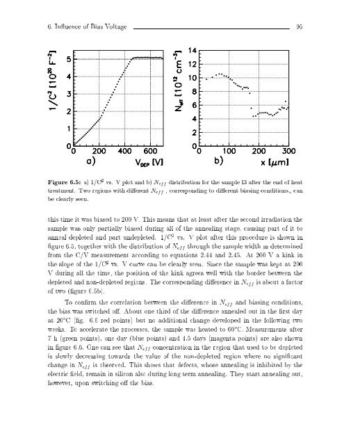
6. Inuence <strong>of</strong> Bias Voltage 95Figure 6.5: a) 1/C 2 vs. V plot and b) N eff distribution <strong>for</strong> the sample I3 after the end <strong>of</strong> heattreatment. Two regions with dierent N eff , correspond<strong>in</strong>g to dierent bias<strong>in</strong>g conditions,, canbe clearly seen.this time it was biased to 200 V. This means that at least after the second ir<strong>radiation</strong> thesample was only partially biased dur<strong>in</strong>g all <strong>of</strong> the anneal<strong>in</strong>g stage, caus<strong>in</strong>g part <strong>of</strong> it toanneal depleted and part undepleted. 1/C 2 vs. V plot after this procedure is shown <strong>in</strong>gure 6.5, together with the distribution <strong>of</strong> N eff through the sample width as determ<strong>in</strong>edfrom the C/V measurement accord<strong>in</strong>g to equations 2.44 and 2.45. At 200 V a k<strong>in</strong>k <strong>in</strong>the slope <strong>of</strong> the 1/C 2 vs. V curve can be clearly seen. S<strong>in</strong>ce the sample was kept at 200V dur<strong>in</strong>g all the time, the position <strong>of</strong> the k<strong>in</strong>k agrees well with the border between thedepleted and non-depleted regions. The correspond<strong>in</strong>g dierence <strong>in</strong> N eff is about a factor<strong>of</strong> two (gure 6.5b).To conrm the correlation between the dierence <strong>in</strong> N eff and bias<strong>in</strong>g conditions,the bias was switched o. About one third <strong>of</strong> the dierence annealed out <strong>in</strong> the rst dayat 20 C (g. 6.6 red po<strong>in</strong>ts) but no additional change developed <strong>in</strong> the follow<strong>in</strong>g twoweeks. To accelerate the processes, the sample was heated to 60 C. Measurements after7 h (green po<strong>in</strong>ts), one day (blue po<strong>in</strong>ts) and 4.5 days (magenta po<strong>in</strong>ts) are also shown<strong>in</strong> gure 6.6. One can see that N eff concentration <strong>in</strong> the region that used to be depletedis slowly decreas<strong>in</strong>g towards the value <strong>of</strong> the non-depleted region where no signicantchange <strong>in</strong> N eff is observed. This shows that defects, whose anneal<strong>in</strong>g is <strong>in</strong>hibited by theelectric eld, rema<strong>in</strong> <strong>in</strong> <strong>silicon</strong> also dur<strong>in</strong>g long term anneal<strong>in</strong>g. They start anneal<strong>in</strong>g out,however, upon switch<strong>in</strong>g o the bias.


