chapter 1 introduction to microprocessor and microcontroller
chapter 1 introduction to microprocessor and microcontroller
chapter 1 introduction to microprocessor and microcontroller

You also want an ePaper? Increase the reach of your titles
YUMPU automatically turns print PDFs into web optimized ePapers that Google loves.
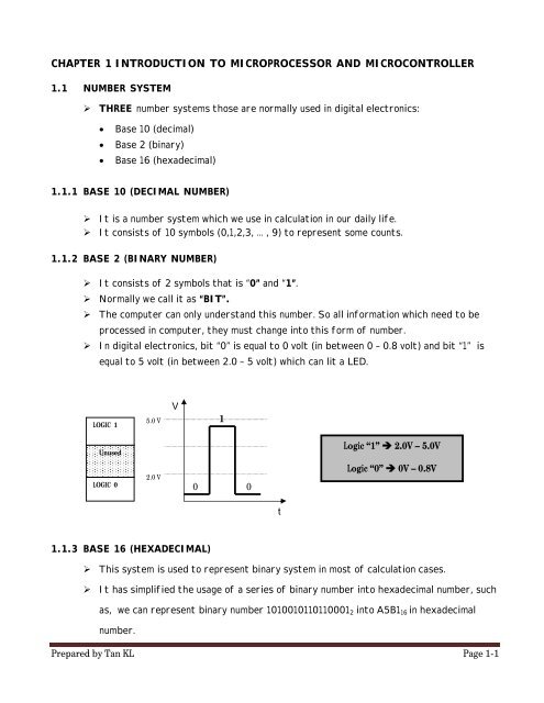
CHAPTER 1 INTRODUCTION TO MICROPROCESSOR AND MICROCONTROLLER1.1 NUMBER SYSTEM‣ THREE number systems those are normally used in digital electronics:Base 10 (decimal)Base 2 (binary)Base 16 (hexadecimal)1.1.1 BASE 10 (DECIMAL NUMBER)‣ It is a number system which we use in calculation in our daily life.‣ It consists of 10 symbols (0,1,2,3, … , 9) <strong>to</strong> represent some counts.1.1.2 BASE 2 (BINARY NUMBER)‣ It consists of 2 symbols that is “0” <strong>and</strong> “1”.‣ Normally we call it as “BIT”.‣ The computer can only underst<strong>and</strong> this number. So all information which need <strong>to</strong> beprocessed in computer, they must change in<strong>to</strong> this form of number.‣ In digital electronics, bit “0” is equal <strong>to</strong> 0 volt (in between 0 – 0.8 volt) <strong>and</strong> bit “1” isequal <strong>to</strong> 5 volt (in between 2.0 – 5 volt) which can lit a LED.LOGIC 15.0 VV1UnusedLogic “1” 2.0V – 5.0VLOGIC 02.0 V0 0Logic “0” 0V – 0.8Vt1.1.3 BASE 16 (HEXADECIMAL)‣ This system is used <strong>to</strong> represent binary system in most of calculation cases.‣ It has simplified the usage of a series of binary number in<strong>to</strong> hexadecimal number, suchas, we can represent binary number 1010010110110001 2 in<strong>to</strong> A5B1 16 in hexadecimalnumber.Prepared by Tan KL Page 1-1
‣ It uses 16 symbols <strong>to</strong> represent a number as shown in the table below:Decimal Binary Hex0 0000 01 0001 12 0010 23 0011 34 0100 45 0101 56 0110 67 0111 78 1000 8Decimal Binary Hex9 1001 910 1010 A11 1011 B12 1100 C13 1101 D14 1110 E15 1111 F1.1.4 NUMBER CONVERTIONDecimal BinaryMethod 1: always divide with “2” <strong>and</strong> collect the remainderExample: Convert 25 10 <strong>to</strong> binary numberResult afterdivision (rounded) remainder25/2 = 12 112/2 = 6 0LSB (Least Significant Bit)6/2 = 3 03/2 = 1 11/2 = 0 1MSB (Most Significant Bit)Hence, 25 10 = 11001 2Method 2: by adding the weight in every bit2 4 2 3 2 2 2 1 2 0 weight16 8 4 2 11 1 0 0 125 10 = 16 + 8 + 1 = 11001 2Prepared by Tan KL Page 1-2
Binary Hexadecimal : collecting 4 bit in one group from the back (LSB)Example: Convert 100111110101 2 <strong>to</strong> Hex number.1001 1111 0101 2= 9 F 5= 9F5 16Hexadecimal Binary : convert every number of Hex <strong>to</strong> 4 bit binaryExample: Convert 29B 16 <strong>to</strong> binary number.2 9 B 16= 0010 1001 1011= 001010011011 2 (“00” in the front can be neglected 1010011011 2 )Decimal Hexadecimal : convert the number in<strong>to</strong> binary first, <strong>and</strong> then in<strong>to</strong>hexadecimalExample : Convert 699 10 <strong>to</strong> Hex2 9 2 8 2 7 2 6 2 5 2 4 2 3 2 2 2 1 2 0512 256 128 64 32 16 8 4 2 11 0 1 0 1 1 1 0 1 12 B B= 2BB 16 (have <strong>to</strong> add “00” in the front <strong>to</strong> make 4 bit in one group)1.1.5 ADDING 2 HEX NUMBORExample: 6 B 16 0110 1011 2+ A F 16 + 1010 1111 21 1 A 16 1 0001 1010 2Carry, C = 1Numbers of “1” is odd, Parity, P = 1Auxiliary Carry, AC = 1Prepared by Tan KL Page 1-3
1.2 BASIC LOGIC GATE1.2.1 AND GATE1.2.2 OR GATE1.2.3 NOT GATEPrepared by Tan KL Page 1-4
1.2.4 EX-OR GATE (Exclusive OR)1.2.5 NAND GATE1.2.6 NOR GATEPrepared by Tan KL Page 1-5
Assignment 1:a. Convert the following numbers <strong>to</strong> Hexadecimal number:i. 11001100 2 ii. 456 10iii. 001110101110 2 iv. 1011 10v. 1110001010 2 vi. 1101 10b. Convert the following numbers <strong>to</strong> binary number:i. 5F6A 16 ii. 127 10iii. 101101 16 iv. 255 10v. FFFF 16 vi. 256 10c. Solve the problems below <strong>and</strong> find out the condition of Carry (C), Auxiliary Carry (AC)<strong>and</strong> Parity (P) bit:i. 5AHex ADD with 36Hex ii. 9DHex ADD with ABHexiii. 8B 16 AND with 97 16 iv. A6 16 AND with C3 16v. A7 16 OR with C1 16 vi. 93 16 OR with C7 16vii. 4C 16 EX-OR with 8A 16 viii. 23 16 EX-OR with EC 16ix. Data 78 16 is OR-ed with data 5C 16 first <strong>and</strong> then is AND-ed with data A7 16x. Data FA 16 is AND-ed with data D8 16 first <strong>and</strong> then EX-OR-ed with data 67 16Prepared by Tan KL Page 1-6
1.3 SAIZ AND UNIT OF DATABit0 1orNibble0 1 0 0Byte 1 0 1 1 0 0 0 1`Word 1 1 0 0 0 0 1 11 0 0 0 1 0 0 0Bit : is the smallest data in digital electronics. It consists of “0” or “1”Byte : data consists of 8 bit or 2 nibble dataNibble : data consists of half byte or 4 bit dataWord : data consists of 2 byte or 4 nibble or 16 bit dataLong Word : data consists of 2 Word or 4 byte or 32 bit dataExample :5 F 9 A Hex 0101 1111 1001 1010 2 16 bit data or 4 nibble data or 2 byte data or 1 Word data or halfLong Word dataPrepared by Tan KL Page 1-7
1.3.1 TERMS FOR MEMORY CAPACITYKilobyte (K) 2 10 Byte (1024 byte)Megabyte (M) 2 20 byte (1,048,576 byte)Gigabyte (G) Gigabyte (G) : 2 30 byte (1,073,741,824 byte) Terabyte (T) : 2 40 byte (???)1.4 THREE COMMON TERMS IN DIGITAL ELECTRONICSMicrocomputerMicroprocessorMicrocontroller1.4.1 BASIC ELEMENTS OF MICROCOMPUTERA complete set of acomputerMemoryOutputControlInpuALUMicroprocessorMicrocomputerPrepared by Tan KL Page 1-8
A microcomputer system consists of the following components:Peripheral InputPeripheral OutputPeripheral S<strong>to</strong>rageCentral Processing Unit1.4.1 Peripheral Input It is a <strong>to</strong>ol <strong>to</strong> be used <strong>to</strong> prepare data or information which will be processed by CentralProcessing Unit. Example: Joystick, Keyboard, Sensor, Scanner1.4.2 Peripheral Output It is a <strong>to</strong>ol <strong>to</strong> be used <strong>to</strong> display data or information which has been processed byCentral Processing Unit. Example: Moni<strong>to</strong>r, Printer, Speaker1.4.3 Peripheral Memory It is a <strong>to</strong>ol <strong>to</strong> be used <strong>to</strong> s<strong>to</strong>re data or information which will be processed or has beenprocessed by Central Processing Unit. Example: Hard disk, CD-ROM, RAM, ROM, Pen drive1.4.4 Central Processing Unit (CPU) It is the most important part in microcomputer system. It acts as a “brain” of amicrocomputer system. It is also called Microprocessor. In here the data are gathered, processed <strong>and</strong> sent out <strong>to</strong> display. It can perform operations such as arithmetic (addition, deduction, multiplication <strong>and</strong>division) <strong>and</strong> logic (AND, OR, NOT etc.) operation <strong>and</strong> make decision after operation. A general internal architecture of a CPU/Microprocessor is shown in the next page. Example: 80486, Pentium II, AMD AtronPrepared by Tan KL Page 1-9
1.4.5 BASIC CONNECTION OF A MICROCOMPUTER SYSTEMPrepared by Tan KL Page 1-10
1.5 MICROPROCESSOR (CPU) It is the most important part in a microcomputer system. It acts as a “brain” of amicrocomputer system. In here the data are gathered, processed <strong>and</strong> put in<strong>to</strong> display through peripheraloutput. It can perform operations such as arithmetic (addition, deduction, multiplication <strong>and</strong>division) <strong>and</strong> logic (AND, OR, NOT etc.) operation <strong>and</strong> make decision after operation.1.5.1 FUNCTION OF COMPONENTS IN A MICROPROCESSORi. ALU (Arithmetic Logic Unit) It performs arithmetic task such as addition, deduction, multiplication <strong>and</strong>division <strong>and</strong> logic task such as AND, OR, NOT <strong>and</strong> etc.Prepared by Tan KL Page 1-11
ii.ACC (Accumula<strong>to</strong>r) It is a register which can s<strong>to</strong>re data for temporary before sending <strong>to</strong> process inALU <strong>and</strong> also can s<strong>to</strong>re the processed data before sending <strong>to</strong> s<strong>to</strong>re in thememory or display through peripheral output. It is just like a “entrance” for a data <strong>to</strong> go in <strong>and</strong> come out from ALU.iii.Flag register/PSW (Program Status Word ) register This register contains information regarding the result of a process which hasbeen carried out by ALU. It tells the user whether the result has Carry (CY), Auxiliary Carry (AC), Odd orEven Parity (P) or Overflow (OV) or the other way round. It also consists information regarding registers from which bank will be workingon (will be discussed further in Chapter 2).iv.Program Counter (PC) It controls the sequence in which the instructions in a program are performed. Normally, it does this by counting in the sequence, that is 0, 1, 2, 3, … At any given time, the count indicates the location in memory from which thenext location of information/instruction is <strong>to</strong> be taken.v. Stack Pointer (SP) This register will s<strong>to</strong>re the contains of Program Counter (location of memory)for a short time when there is subroutine/sub-program occurs in the program. This register will be taken place when some particular instructions, such asPUSH, POP, CALL <strong>and</strong> RET are used in the program.vi.Data Register This register is a temporary s<strong>to</strong>rage location for data going <strong>to</strong> or coming fromthe data bus.Prepared by Tan KL Page 1-12
vii.Address Register This register is another temporary s<strong>to</strong>rage location. It holds the address of the memory location or I/O device that is used in theoperation presently being performed.viii.Instruction Decoder After an data is pulled from memory <strong>and</strong> placed in the data register, the data isdecoded by this circuit. The decoder checks the code <strong>and</strong> decides which operation is <strong>to</strong> be performed.ix.Controller-sequencer This unit will produce a variety of control signals <strong>to</strong> carry out the instruction. Since each instruction is different, a different combination of control signals isproduced for each instruction.x. Data Bus It is a group of wires that is used <strong>to</strong> channel data (which <strong>to</strong> be processed orafter processed) from peripherals (memory or I/O devices) <strong>to</strong> CPU or vice versa.xi.Address Bus It is a group of wires that is used <strong>to</strong> channel locations of data which will be orhas been processed.xii.Control Bus It is a group of wires that is used <strong>to</strong> send control signals (such as MEMW,MEMR, IOR, IOW, interrupt <strong>and</strong> DMA) from CPU <strong>to</strong> peripheral (memory or I/Odevices) or vice versa.Prepared by Tan KL Page 1-13
1.6 MICROCONTROLLER (MC) It is also called computer in a single chip. Inside MC we can find the important components which are needed in microcomputersystem, such as CPU, RAM, ROM <strong>and</strong> peripheral I/O.Prepared by Tan KL Page 1-14
1.6.1 THE DIFFERENCES BETWEEN MICROPROCESSOR AND MICROCONTROLLERMicroprocessorMicrocontroller1. CPU, ROM, RAM, timer <strong>and</strong> I/O devices areall in seperated unit.1. CPU, ROM, RAM, timer <strong>and</strong> I/O devicesare all in a chip (Embedded in a chip).2. System designer can determine the capasityfor RAM, ROM <strong>and</strong> I/O devices.2. Capacity of RAM,ROM <strong>and</strong> I/O deviceshave been determined during fabrication.3. Capacity of memory <strong>and</strong> I/O port can beadded (expansived) at any time.3. Capacity of memory <strong>and</strong> I/O port cannotbe added (expansived) at any time.4. Suitable for project which has exp<strong>and</strong>edspace.4. Suitable for project which has limitedspace.5. For general-purposes usages4. For specific-purposes usages1.7 Evolution Of MicroprocessorNameDate Transis<strong>to</strong>rs MicronsClockspeedDatawidthMIPS8080 1974 6,000 6 2 MHz 8 bits 0.648088 1979 29,000 3 5 MHz16 bits8-bitbus0.3380286 1982 134,000 1.5 6 MHz 16 bits 180386 1985 275,000 1.5 16 MHz 32 bits 580486 1989 1,200,000 1 25 MHz 32 bits 20Pentium 1993 3,100,000 0.8 60 MHz32 bits64-bitbus100Prepared by Tan KL Page 1-15
Pentium II 1997 7,500,000 0.35233MHz32 bits64-bitbus~300Pentium III 1999 9,500,000 0.25450MHz32 bits64-bitbus~510Pentium 4 2000 42,000,000 0.18 1.5 GHz32 bits64-bitbus~1,700Pentium 4"Prescott"2004 125,000,000 0.09 3.6 GHz32 bits64-bitbus~7,000The date is the year that the processor was first introduced. Many processors are reintroducedat higher clock speeds for many years after the original release date.Transis<strong>to</strong>rs is the number of transis<strong>to</strong>rs on the chip. You can see that the number oftransis<strong>to</strong>rs on a single chip has risen steadily over the years.Microns is the width, in microns, of the smallest wire on the chip. For comparison, a humanhair is 100 microns thick. As the feature size on the chip goes down, the number oftransis<strong>to</strong>rs rises.Clock speed is the maximum rate that the chip can be clocked at. Clock speed will makemore sense in the next section. Data Width is the width of the ALU. An 8-bit ALU can add/subtract/multiply/etc. two 8-bit numbers, while a 32-bit ALU can manipulate 32-bit numbers. An 8-bit ALU would have<strong>to</strong> execute four instructions <strong>to</strong> add two 32-bit numbers, while a 32-bit ALU can do it inone instruction. In many cases, the external data bus is the same width as the ALU, butnot always. The 8088 had a 16-bit ALU <strong>and</strong> an 8-bit bus, while the modern Pentiums fetchdata 64 bits at a time for their 32-bit ALUs.MIPS st<strong>and</strong>s for "millions of instructions per second" <strong>and</strong> is a rough measure of theperformance of a CPU. Modern CPUs can do so many different things that MIPS ratingslose a lot of their meaning, but you can get a general sense of the relative power of theCPUs from this column.Prepared by Tan KL Page 1-16
Exercise:a. List out 4 important components of a microcomputer system <strong>and</strong> briefly describe theirfunctions.b. Describe briefly the functions for the components below:i. Address Busii.iii.Data BusControl Busc. Draw a block diagram of a <strong>microprocessor</strong> <strong>and</strong> briefly describe function of it’s component.d. State the differences between <strong>microprocessor</strong> <strong>and</strong> <strong>microcontroller</strong>.e. State the function for the components below:i. ALU iv. Stack Pointerii. Accumula<strong>to</strong>r v. Program Status Word Registeriii. Program Counter vi. Controller Sequencerf. Different <strong>microprocessor</strong>s have different data bus such as 8-bit, 16-bit <strong>and</strong> 32-bit. State2 advantages <strong>and</strong> 2 disadvantages of a smaller size of data bus as compared <strong>to</strong> a wider sizeof data bus of <strong>microprocessor</strong>s.Prepared by Tan KL Page 1-17
1.7 EXECUTING A PROGRAM Before a program can be run, it must be placed in memory. There are 2 phases involving in executing a program, those are the fetch phase <strong>and</strong>the executing phase.CARRYFLAGACCUMULATORALUControl Unit(ControllerSequencer)CLOCK <strong>and</strong>CONTROLLINESPROGRAMCOUNTER(PC)InstructionDecoderADDRESSREGISTER(AR)DATAREGISTER(DR)HEX00H01H02H03H04H05H06HADDRESS CODE00000000 0111010000000001 0001000000000010 0010010000000011 0000011100000100 1111010100000101 0011000000000110 11110100MEMORYExample:MOV A, #10HADD A, #07HMOV 30H, AMOV A, #10HBinary code whichrepresents a programProgramPrepared by Tan KL Page 1-18
To execute a program, the program needs <strong>to</strong> s<strong>to</strong>re in memory first, that is inProgram/Code Memory (ROM). This means that the program needs <strong>to</strong> be translated in<strong>to</strong>the machine language (binary code) <strong>and</strong> s<strong>to</strong>red in the memory. The program will be executed step-by-step from the first address which is 00000000B(00H). This first address (00H) will be always referred by MP when there is RESET operationis carring out.The Fetching Phase** The phase which CPU fetches the instruction from main memory via the data bus in<strong>to</strong>the Instruction Register (IR) so that it can be decoded <strong>and</strong> executedi. When the Microprocessor (MP) is ON-ed, the contain of Program Counter (PC) isset <strong>to</strong> the first address, that is 00H au<strong>to</strong>matically.ii.Then, this address is passed <strong>to</strong> the Address Register (AR = 00H).iii.The contain of PC is incremented by 1 au<strong>to</strong>matically. So the contain of PC is 01Hnow.iv.The contain of AR (00H) is placed on the Address Bus so that the MP will go <strong>to</strong> theaddressed location <strong>to</strong> obtain the data in the addressed location, which is 00H.v. Then, the data which is in the location of 00H is passed through the Data Bus <strong>and</strong>send <strong>to</strong> the Data Register (DR) which is inside the MP.vi.From the DR, the data is passed <strong>to</strong> the Instruction Decoder <strong>to</strong> interpret the data.vii.In this case, the instruction MOV A (with code = 01110100B) is interpreted, that is,moving/copying something in<strong>to</strong> Accumula<strong>to</strong>r (”A” st<strong>and</strong>s for Accumula<strong>to</strong>r).Prepared by Tan KL Page 1-19
viii.Following this, the Control Unit (Controller Sequencer) produces control signals <strong>to</strong>get the data which is in the following location of memory (01H) <strong>and</strong> place it in<strong>to</strong>Accumula<strong>to</strong>r, as what has requested by the instruction.The Execute Phase In this phase, CPU will carry out the requirement on the instruction. In this case, theCPU will move/copy data in<strong>to</strong> Accumula<strong>to</strong>r.i. The contain of PC (01H) is sent <strong>to</strong> AR (AR = 01H).ii.The contain of PC, as usual is incremented by 1 <strong>and</strong> become 02H now.iii.The contain of AR is placed on the Address Bus. Then, the location of the memoryis identified, which is 02H.iv.The data in the location of 02H is placed on Data Bus <strong>and</strong> is sent <strong>to</strong> the DR in theMP.v. From DR, the data straight away sends <strong>to</strong> Accumula<strong>to</strong>r as what has requestedbefore (MOV A).vi.So, now the data ”10H” is inside the Accumula<strong>to</strong>r. The instruction ”MOV A, #10H”has been executed.vii.These program-executional steps will be the same for any other instruction.1.8 TERMS OF PROCESSING DATA IN MICROPROCESSORInstruction Cycle It is the process by which a computer retrieves a program instruction from its memory,determine what actions the instruction required, <strong>and</strong> carry out the actions. This cycle is repeated continuously by the CPU, from booting up <strong>to</strong> shutting down of acomputer.Prepared by Tan KL Page 1-20
Exercise:a. With the help of a suitable block diagram, explain briefly the steps <strong>to</strong> execute ”ADD A,#74H”.Prepared by Tan KL Page 1-21