MPX5010 Data Sheet
MPX5010 Data Sheet
MPX5010 Data Sheet
- No tags were found...

You also want an ePaper? Increase the reach of your titles
YUMPU automatically turns print PDFs into web optimized ePapers that Google loves.
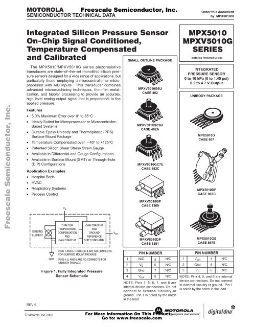
Freescale Semiconductor, Inc.SEMICONDUCTOR TECHNICAL DATAOrder this documentby <strong>MPX5010</strong>/Dnc...Freescale Semiconductor, I The <strong>MPX5010</strong>/MPXV5010G series piezoresistivetransducers are state–of–the–art monolithic silicon pressuresensors designed for a wide range of applications, butparticularly those employing a microcontroller or microprocessorwith A/D inputs. This transducer combinesadvanced micromachining techniques, thin–film metallization,and bipolar processing to provide an accurate,high level analog output signal that is proportional to theapplied pressure.Features• 5.0% Maximum Error over 0° to 85°C• Ideally Suited for Microprocessor or Microcontroller–Based Systems• Durable Epoxy Unibody and Thermoplastic (PPS)Surface Mount Package• Temperature Compensated over 40° to +125°C• Patented Silicon Shear Stress Strain Gauge• Available in Differential and Gauge Configurations• Available in Surface Mount (SMT) or Through–hole(DIP) ConfigurationsApplication Examples• Hospital Beds• HVAC• Respiratory Systems• Process Control SMALL OUTLINE PACKAGEMPXV5010G6UCASE 482MPXV5010GC6UCASE 482AMPXV5010GC7UCASE 482CMPXV5010GPCASE 1369MPXV5010DPCASE 1351Motorola Preferred DeviceINTEGRATEDPRESSURE SENSOR0 to 10 kPa (0 to 1.45 psi)0.2 to 4.7 V OutputUNIBODY PACKAGE<strong>MPX5010</strong>DCASE 867<strong>MPX5010</strong>DPCASE 867C<strong>MPX5010</strong>GSCASE 867EREV 9 Figure 1. Fully Integrated PressureSensor SchematicPIN NUMBER123N/CV SGnd567N/CN/CN/C4 V out 8 N/CNOTE: Pins 1, 5, 6, 7, and 8 areinternal device connections. Do notconnect to external circuitry orground. Pin 1 is noted by the notchin the lead.123PIN NUMBERV out 4Gnd 5V S 6N/CN/CN/CNOTE: Pins 4, 5, and 6 are internaldevice connections. Do not connectto external circuitry or ground. Pin 1is noted by the notch in the lead.© Motorola, Motorola Inc. Sensor 2002 Device <strong>Data</strong>For More Information On This Product,Go to: www.freescale.com1
MAXIMUM RATINGS (NOTE) Parametrics Symbol Value Unit Freescale Semiconductor, Inc.Maximum Pressure (P1 > P2) P max 75 kPaStorage Temperature T stg –40 to +125 °COperating Temperature T A –40 to +125 °CNOTE: Exposure beyond the specified limits may cause permanent damage or degradation to the device.nc...Freescale Semiconductor, IOPERATING CHARACTERISTICS (V S = 5.0 Vdc, T A = 25°C unless otherwise noted, P1 > P2. Decoupling circuit shown in Figure 3required to meet specification.)Characteristic Symbol Min Typ Max UnitPressure Range (1) P OP 0 — 10 kPaSupply Voltage (2) V S 4.75 5.0 5.25 VdcSupply Current I o — 5.0 10 mAdcMinimum Pressure Offset (3)(0 to 85°C)V off 0 0.2 0.425 Vdc@ V S = 5.0 VoltsFull Scale Output (4)@ V S = 5.0 VoltsFull Scale Span (5)@ V S = 5.0 Volts(0 to 85°C)(0 to 85°C)V FSO 4.475 4.7 4.925 VdcV FSS 4.275 4.5 4.725 VdcAccuracy (6) (0 to 85°C) — — — ±5.0 %V FSSSensitivity V/P — 450 — mV/kPaResponse Time (7) t R — 1.0 — msOutput Source Current at Full Scale Output I O+ — 0.1 — mAdcWarm–Up Time (8) — — 20 — msOffset Stability (9) — — ±0.5 — %V FSSNOTES:1. 1.0 kPa (kiloPascal) equals 0.145 psi.2. Device is ratiometric within this specified excitation range.3. Offset (V off ) is defined as the output voltage at the minimum rated pressure.4. Full Scale Output (V FSO ) is defined as the output voltage at the maximum or full rated pressure.5. Full Scale Span (V FSS ) is defined as the algebraic difference between the output voltage at full rated pressure and the output voltage at theminimum rated pressure.6. Accuracy (error budget) consists of the following:• Linearity: Output deviation from a straight line relationship with pressure over the specified pressure range.• Temperature Hysteresis: Output deviation at any temperature within the operating temperature range, after the temperature iscycled to and from the minimum or maximum operating temperature points, with zero differential pressureapplied.• Pressure Hysteresis: Output deviation at any pressure within the specified range, when this pressure is cycled to and from theminimum or maximum rated pressure, at 25°C.• TcSpan: Output deviation over the temperature range of 0° to 85°C, relative to 25°C.• TcOffset: Output deviation with minimum rated pressure applied, over the temperature range of 0° to 85°C, relativeto 25°C.• Variation from Nominal: The variation from nominal values, for Offset or Full Scale Span, as a percent of V FSS , at 25°C.7. Response Time is defined as the time for the incremental change in the output to go from 10% to 90% of its final value when subjected toa specified step change in pressure.8. Warm–up Time is defined as the time required for the product to meet the specified output voltage after the Pressure has been stabilized.9. Offset Stability is the product’s output deviation when subjected to 1000 hours of Pulsed Pressure, Temperature Cycling with Bias Test.MECHANICAL CHARACTERISTICSCharacteristics Typ UnitWeight, Basic Element (Case 867) 4.0 gramsWeight, Basic Element (Case 482) 1.5 grams2 For More Information On This Product, Motorola Sensor Device <strong>Data</strong>Go to: www.freescale.com
Freescale Semiconductor, Inc. ON–CHIP TEMPERATURE COMPENSATION, CALIBRATION AND SIGNAL CONDITIONINGThe performance over temperature is achieved by integratingthe shear–stress strain gauge, temperature compensation,calibration and signal conditioning circuitry onto a singlemonolithic chip.Figure 2 illustrates the Differential or Gauge configuration inthe basic chip carrier (Case 482). A fluorosilicone gel isolatesthe die surface and wire bonds from the environment, whileallowing the pressure signal to be transmitted to the sensordiaphragm.The <strong>MPX5010</strong> and MPXV5010G series pressure sensoroperating characteristics, and internal reliability and qualificationtests are based on use of dry air as the pressure media.Media, other than dry air, may have adverse effects onsensor performance and long–term reliability. Contact thefactory for information regarding media compatibility in yourapplication.Figure 3 shows the recommended decoupling circuit for interfacingthe integrated sensor to the A/D input of a microprocessoror microcontroller. Proper decoupling of the powersupply is recommended.Figure 4 shows the sensor output signal relative to pressureinput. Typical, minimum, and maximum output curvesare shown for operation over a temperature range of 0° to85°C using the decoupling circuit shown in Figure 4. Theoutput will saturate outside of the specified pressure range.nc...Freescale Semiconductor, I Figure 2. Cross–Sectional Diagram SOP(Not to Scale) ± ° Figure 3. Recommended power supply decouplingand output filtering.For additional output filtering, please refer toApplication Note AN1646. Figure 4. Output versus Pressure DifferentialMotorola Sensor Device <strong>Data</strong>For More Information On This Product,Go to: www.freescale.com3
Transfer Function (<strong>MPX5010</strong>, MPXV5010G)Freescale Semiconductor, Inc.Nominal Transfer Value: V out = V S x (0.09 x P + 0.04)Nominal Transfer Value: ± (Pressure Error x Temp. Factor x 0.09 x V S )Nominal Transfer Value: V S = 5.0 V ± 0.25 VdcTemperature Error Band<strong>MPX5010</strong>, MPXV5010G Seriesnc...Freescale Semiconductor, IPressure Error Band °NOTE: The Temperature Multiplier is a linear response from 0° to –40°C and from 85° to 125°C. ± 4 For More Information On This Product, Motorola Sensor Device <strong>Data</strong>Go to: www.freescale.com
PRESSURE (P1)/VACUUM (P2) SIDE IDENTIFICATION TABLEMotorola designates the two sides of the pressure sensoras the Pressure (P1) side and the Vacuum (P2) side. ThePressure (P1) side is the side containing fluoro silicone gelwhich protects the die from harsh media. The Motorola MPXFreescale Semiconductor, Inc. pressure sensor is designed to operate with positive differentialpressure applied, P1 > P2.The Pressure (P1) side may be identified by using the tablebelow:nc...Freescale Semiconductor, IPart NumberCase Type<strong>MPX5010</strong>D 867C Stainless Steel Cap<strong>MPX5010</strong>DP 867C Side with Part Marking<strong>MPX5010</strong>GP 867B Side with Port Attached<strong>MPX5010</strong>GS 867E Side with Port Attached<strong>MPX5010</strong>GSX 867F Side with Port AttachedMPXV5010G6U 482 Stainless Steel CapMPXV5010G7U 482B Stainless Steel CapMPXV5010GC6U/T1 482A Side with Port AttachedMPXV5010GC7U 482C Side with Port AttachedMPXV5010GP 1369 Side with Port AttachedMPXV5010DP 1351 Side with Part MarkingORDERING INFORMATION — UNIBODY PACKAGE (<strong>MPX5010</strong> SERIES)Pressure (P1)Side IdentifierMPX SeriesDevice Type Options Case Type Order Number Device MarkingBasic Element Differential 867 <strong>MPX5010</strong>D <strong>MPX5010</strong>DPorted Elements Differential, Dual Port 867C <strong>MPX5010</strong>DP <strong>MPX5010</strong>DPGauge 867B <strong>MPX5010</strong>GP <strong>MPX5010</strong>GPGauge, Axial 867E <strong>MPX5010</strong>GS <strong>MPX5010</strong>DGauge, Axial PC Mount 867F <strong>MPX5010</strong>GSX <strong>MPX5010</strong>DORDERING INFORMATION — SMALL OUTLINE PACKAGE (MPXV5010G SERIES)Device Type Options Case No. MPX Series Order No. Packing Options MarkingBasic Elements Gauge, Element Only, SMT 482 MPXV5010G6U Rails MPXV5010GGauge, Element Only, DIP 482B MPXV5010G7U Rails MPXV5010GPorted Elements Gauge, Axial Port, SMT 482A MPXV5010GC6U Rails MPXV5010GGauge, Axial Port, DIP 482C MPXV5010GC7U Rails MPXV5010GGauge, Axial Port, SMT 482A MPXV5010GC6T1 Tape and Reel MPXV5010GGauge, Side Port, SMT 1369 MPXV5010GP Trays MPXV5010GDifferential, Dual Port, SMT 1351 MPXV5010DP Trays MPXV5010GMotorola Sensor Device <strong>Data</strong>For More Information On This Product,Go to: www.freescale.com5
MINIMUM RECOMMENDED FOOTPRINT FOR SURFACE MOUNTED APPLICATIONSSurface mount board layout is a critical portion of the totaldesign. The footprint for the surface mount packages mustbe the correct size to ensure proper solder connection interfacebetween the board and the package. With the correctFreescale Semiconductor, Inc.footprint, the packages will self align when subjected to asolder reflow process. It is always recommended to designboards with a solder mask layer to avoid bridging and shortingbetween solder pads.nc...Freescale Semiconductor, IFigure 5. SOP Footprint (Case 482)6 For More Information On This Product, Motorola Sensor Device <strong>Data</strong>Go to: www.freescale.com
Freescale Semiconductor, Inc. SMALL OUTLINE PACKAGE DIMENSIONSnc...Freescale Semiconductor, I–B–JKN –B–J–A–SN–A–SMVGCGCD 8 PL D 8 PLPIN 1 IDENTIFIERCASE 482–01ISSUE O W HH–T––T– KMPIN 1 IDENTIFIERCASE 482A–01ISSUE AMotorola Sensor Device <strong>Data</strong>For More Information On This Product,Go to: www.freescale.com7
Freescale Semiconductor, Inc.SMALL OUTLINE PACKAGE DIMENSIONS—CONTINUEDnc...Freescale Semiconductor, IN–B–J–A–SGVCMDETAIL X PIN 1IDENTIFIERD 8 PL WCASE 482C–03ISSUE BDETAIL XK–T– 8 For More Information On This Product, Motorola Sensor Device <strong>Data</strong>Go to: www.freescale.com
Freescale Semiconductor, Inc.SMALL OUTLINE PACKAGE DIMENSIONS—CONTINUED AEee/2D.014 (0.35)θLDETAIL GA1nc...FBE1 b Freescale Semiconductor, IP∅ TDETAIL GNACMKCASE 1369–01ISSUE O θ ° ° ° °Motorola Sensor Device <strong>Data</strong>For More Information On This Product,Go to: www.freescale.com9
Freescale Semiconductor, Inc.SMALL OUTLINE PACKAGE DIMENSIONS—CONTINUEDAEee/2D.014 (0.35)θLDETAIL GA1nc...FBE1 b Freescale Semiconductor, IPNDETAIL GACM∅ TKCASE 1351–01ISSUE O θ ° ° ° °10 For More Information On This Product, Motorola Sensor Device <strong>Data</strong>Go to: www.freescale.com
Freescale Semiconductor, Inc.UNIBODY PACKAGE DIMENSIONS nc...Freescale Semiconductor, IBJSPORT #1POSITIVEPRESSURE(P1)PORT #2VACUUM(P2)CXM–A–P RC –T– –T–JNBPIN 1 –T–F PIN 1R D 6 PLGNL GPOSITIVE PRESSURE(P1)CASE 867–08ISSUE NBASIC ELEMENT F–A–UWLVCASE 867C–05ISSUE FD 6 PL PORT #2 VACUUM (P2)PORT #1 POSITIVEPRESSURE (P1)–Q–S K PRESSURE AND VACUUM SIDES PORTED (DP)Motorola Sensor Device <strong>Data</strong>For More Information On This Product,Go to: www.freescale.com11
Freescale Semiconductor, Inc.UNIBODY PACKAGE DIMENSIONS—CONTINUEDCA nc...Freescale Semiconductor, I–B–VPORT #1POSITIVEPRESSURE(P1)NE–T–JKSG FCASE 867E–03ISSUE DD 6 PLPIN 1PRESSURE SIDE PORTED (AS, GS) 12 For More Information On This Product, Motorola Sensor Device <strong>Data</strong>Go to: www.freescale.com
Freescale Semiconductor, Inc.NOTES Freescale Semiconductor, Inc...Motorola Sensor Device <strong>Data</strong>For More Information On This Product,Go to: www.freescale.com13
Freescale Semiconductor, Inc.NOTESFreescale Semiconductor, Inc...14 For More Information On This Product, Motorola Sensor Device <strong>Data</strong>Go to: www.freescale.com
Freescale Semiconductor, Inc.NOTES Freescale Semiconductor, Inc...Motorola Sensor Device <strong>Data</strong>For More Information On This Product,Go to: www.freescale.com15
Freescale Semiconductor, Inc.nc...Freescale Semiconductor, IMotorola reserves the right to make changes without further notice to any products herein. Motorola makes no warranty, representation or guarantee regardingthe suitability of its products for any particular purpose, nor does Motorola assume any liability arising out of the application or use of any product or circuit,and specifically disclaims any and all liability, including without limitation consequential or incidental damages. “Typical” parameters can and do vary in differentapplications and actual performance may vary over time. All operating parameters, including “Typicals” must be validated for each customer application bycustomer’s technical experts. Motorola does not convey any license under its patent rights nor the rights of others. Motorola products are not designed,intended, or authorized for use as components in systems intended for surgical implant into the body, or other applications intended to support or sustain life,or for any other application in which the failure of the Motorola product could create a situation where personal injury or death may occur. Should Buyer purchaseor use Motorola products for any such unintended or unauthorized application, Buyer shall indemnify and hold Motorola and its officers, employees,subsidiaries, affiliates, and distributors harmless against all claims, costs, damages, and expenses, and reasonable attorney fees arising out of, directly orindirectly, any claim of personal injury or death associated with such unintended or unauthorized use, even if such claim alleges that Motorola was negligentregarding the design or manufacture of the part. Motorola and the Stylized M Logo are registered trademarks of Motorola, Inc. Motorola, Inc. is an EqualOpportunity/Affirmative Action Employer.MOTOROLA and the Stylized M Logo are registered in the US Patent & Trademark Office. All other product or service names are the property of their respectiveowners. Motorola, Inc. 2002.How to reach us:USA/EUROPE/Locations Not Listed: Motorola Literature Distribution; P.O. Box 5405, Denver, Colorado 80217. 1–303–675–2140 or 1–800–441–2447JAPAN: Motorola Japan Ltd.; SPS, Technical Information Center, 3–20–1, Minami–Azabu. Minato–ku, Tokyo 106–8573 Japan. 81–3–3440–3569ASIA/PACIFIC: Motorola Semiconductors H.K. Ltd.; Silicon Harbour Centre, 2 Dai King Street, Tai Po Industrial Estate, Tai Po, N.T., Hong Kong. 852–26668334Technical Information Center: 1–800–521–6274HOME PAGE: http://www.motorola.com/semiconductors/16 Motorola Sensor Device <strong>Data</strong>◊For More Information On This Product,<strong>MPX5010</strong>/DGo to: www.freescale.com