

section - Bitsavers
section - Bitsavers
section - Bitsavers
- No tags were found...

Create successful ePaper yourself
Turn your PDF publications into a flip-book with our unique Google optimized e-Paper software.
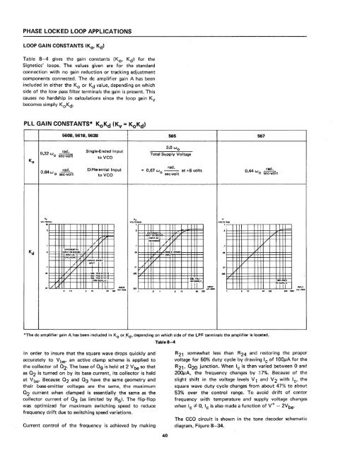
PHASE LOCKED LOOP APPLICATION.SLOOP GAIN CONSTANTS (K o , Kd)Table 8-4 gives the gain constants (K o , Kd) for theSignetics' loops. The values given are for the standardconnection with no gain reduction or tracking adjustmentcomponents connected. The dc amplifier gain A has beenincluded in either the Ko or Kd value, depending on whichside of the low pass filter terminals the gain is present. Thiscauses no hardship in calculations since the loop gain Kvbecomes simply KoKd.5608,5618,5628 565 567Korad.Single-Ended Input0.32 Wo sec-voltto veo3.0w oTotal Supply Voltagerad.rad. Differential Inputrad.O.64w = 0.67 Wo --- at ±6 volts 0.44 Woo sec-volt to veo sec-volt sec-voltKdKdVOLTS/RAD,DKdVOLTSIRAD,KVOLTS.QAD,5 .5DIFFEAENTIAL-./~TORSECONDGROUNDEi/'//, .,DIFFERENTIAL /' VIIL.-_l-L...-.5 I I--/ ./INPUT";;- VVI/.,[7 17.• r-f- INPUT OR SECOND .06 / /SINGLE-ENDED.06r-f- INPUT ACINl'UT./r-r- GROUNDED ./SlNGLE-EYEi r- V// INiT 1/ /.D'/., .D, ./ ///.06 V .L plls,1 TO'.-.006V.006./.. '.D .'D.D' / /V II INPUT.00'50100 MV-RMS ., .. , • .68'- PINS" TO ,.-ic~8~:~L~~ ,'-681-PIN7-TiiLV,'D 110 ,00 1/v1,/6I1-PIN2INPUT riiT- INPUTmV-AMS500 1000 mV-RMSlD 50'00V*The de amplifier gain A has been included in Ko or $d' depending on which side of the LPF terminals the amplifier is located.Table 8-4In order to insure that the square wave drops quickly andaccurately to Vbe, an active clamp scheme is applied tothe collector of 02. The base of 09 is held at 2 V be so thatas 02 is turned on by its base current, its collector is heldat V be. Because 02 and 03 have the same geometry andtheir base-emitter voltages are the same, the maximum02 current when clamped is essentially the same as thecollector current of 03 (as limited by R5). The flip-flopwas optimized for maximum switching speed to reducefrequency drift due to switching speed variations.Current control of the frequency is achieved by makingR21 somewhat less than R24 and restoring the propervoltage for 50% duty cycle by drawing Ic of 100,uA for theR21, 020 junction. When Ic is then varied between 0 and200,uA, the frequency changes by ±7%. Because of theslight shift in the voltage levels V 1 and V 2 with Ic, thesquare wave duty cycle changes from about 47% to about53% over the control range. To avoid drift of centerfrequency with temperature and supply voltage changeswhen Ic =1= 0, Ic is also made a function of V+ - 2Vbe·The CCO circuit is shown in the tone decoder schematicdiagram, Figure 8-34.40


