A Double ZVS-PWM Active-Clamping Forward Converter ... - Ivo Barbi
A Double ZVS-PWM Active-Clamping Forward Converter ... - Ivo Barbi
A Double ZVS-PWM Active-Clamping Forward Converter ... - Ivo Barbi
- No tags were found...

You also want an ePaper? Increase the reach of your titles
YUMPU automatically turns print PDFs into web optimized ePapers that Google loves.
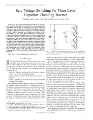
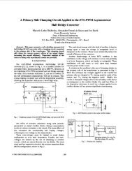
Turn off: In this case, it is analyzed the turn-off of theswitch SI which happens in the second and third stages.During this switching, the resonant capacitor Crl is charged.The equation (1 1) is also obtained for no load operationcondition of the converter. Therefore,eoff =@,*toff (12)Displacement angle eon as function of T during the turnoffis shown in Fig. 5.@a 24Id1 222,I1.61.41.10..I06L.1) Resonant inductor L,: The resonant inductor isdefined by the specified maximum reduction of duty cycleand is calculated from (5).*AD,, 200 .0.2L, = 2. f. . n .I, .(2 - 0-) = 2.1. lo5 .0.6.50. (2 - 0.8)= 5.6pH2) <strong>Clamping</strong> capacitor CC: To determine the capacitanceit is consider that the resonance period of the clampingcapacitor and resonance inductor is three times the switchingperiod Ts. Therefore,2. x . = 3. T,3) Resonant capacitor C,: To determine the capacitanceit is necessary to find the oscillation frequency between L,and C,. For this purpose, Fig 5 and equation (13)-are used.From the curve of Dmi,=0.65, values of Bo@ and f are:8, = 0.56radf = 0.1From equation (13), the commutation time is:020 o om am am an 0.12 a14 016 at, 02- tFig. 5. Displacement angle 8, asfunction of 7 during turn-off.The charge time of the resonant capacitor Crl is given byIv. SIMPLIFIED DESIGN EXAMPLEA methodology and design procedure is presented in thissection.The oscillation frequency is obtained from equation (12).15.6 1 lo6 (2. x a1 IO6)'= 4.6nFA. Input DataCO == 17pFP.X.~,.AV, 2.x.1.10~ .0.48P0=3000w output power;Maximum allowable series resistance of output capacitor2Vi=400V input voltage;CO must be:V0=60Voutput voltage;AVO 0,48RSE = - - = 0,096Q10=50A output current;AkO 5f,=1 OOkHZ switching frequency. C. Semiconductors voltage and current stressesB. Determination of passive componentsAssuming ideal switches and diodes .and considering:Dm, =0.8maximum duty cycleAD- =0.2maximum duty cycle reductionThe transformer turns ratio is calculated from (6)n-NS - (2-D") .%- (2-0.8) 60 - o.6N, (Dmx-ADw) V, (0.8-0.2) 200The clamping voltage is calculated from (1)2V, = .Vi = -. 200=333.34\/(2- Dmx) (2- 0.8)c, =4) Output filter: The output filter can be calculated in thesame way as for a conventional hll-bridge converter. Thisfilter is designed for a maximum current ripple AIh=5A (1 0%of I,) and a maximum voltage ripple AV,=0.48 (0.8% of Vo).A', = 51) Main and auxiliary switches: the maximum voltageacross the blocking switches is:vs,szs,, = - 2.V = -= 2.200 333.34u(2-D-) (2-0.8)The rms current through the main switches (SI, Sz) andauxiliary switches (S3, S4) can be calculated by means of thenormalized current values determined in [7]; for AD,,=0.2we have:Isr.sz, = 0.041s3.s4m, = 0.015Hence,599