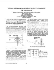
A Double ZVS-PWM Active-Clamping Forward Converter ... - Ivo Barbi
A Double ZVS-PWM Active-Clamping Forward Converter ... - Ivo Barbi
A Double ZVS-PWM Active-Clamping Forward Converter ... - Ivo Barbi
- No tags were found...

Create successful ePaper yourself
Turn your PDF publications into a flip-book with our unique Google optimized e-Paper software.
A DOUBLE <strong>ZVS</strong>-<strong>PWM</strong> ACTIVE-CLAMPING FORWARD CONVERTERRenC Tonico BascopC and <strong>Ivo</strong> <strong>Barbi</strong>FEDERAL UNIVERSITY OF SANTA CATARINADepartment of Electrical EngineeringPower Electronic InstituteP. 0. Box. 51 1988.040-970 - Floriandpolis - SC - BrazilTel.: (55)48-331.9204 - Fax: (55) 48-234.5422E-mail: ivo@inep.ufsc.br; rene@inep.ufsc.brAbstract - This paper presents a new isolated dc-dcconverter, named <strong>Double</strong> <strong>ZVS</strong>-<strong>PWM</strong> <strong>Active</strong>-<strong>Clamping</strong><strong>Forward</strong> <strong>Converter</strong>, which operates without switching lossesfrom no-load up to hll-load. The proposed converter is basedon two active-clamping forward converters, coupled with asingle high frequency transformer. This converter is suitablefor high input voltage and high power applications. Operationprinciple, theoretical analysis, design example andexperimental results, taken from a 3kW laboratory prototype,are presented.I. INTRODUCTIONhand, they are capable of automatically balance the voltage ofthe input capacitors associated in series and connected to a dcbus voltage. If one of the voltages is higher, the respectivecapacitor will transfer energy to the other through thetransformer during the on time.In this paper we propose the converter shown in Fig. 1.The converter is composed of two active-clamping <strong>ZVS</strong>-<strong>PWM</strong> forward converters coupled by single transformer. Theproposed converter was derived from the topologies proposedin references [5, 61. This converter is described and analyzedin the following sections.Nowadays, the most used power converter topology inhigh power dc-dc power supplies applications is the fullbridgezero-voltage-switching pulse-width-modulation (FB-<strong>ZVS</strong>-<strong>PWM</strong>) converter. It is considered one of the bestalternative for high power applications and its control strategyis well known. This converter possesses the most desirablecharacteristic of both, the hard switching <strong>PWM</strong> and the softswitching resonant converters, avoiding their majordrawbacks, such as commutation losses in the first mode andvariable switching frequency and high conduction losses inthe second mode[ 11.However, the conventional FB-<strong>ZVS</strong>-<strong>PWM</strong> converter isnot suitable for high input voltage applications because thetotal input voltage is applied across its blocking switches.Among the alternatives to overcome this drawbacks arethe series connection of switches and multilevel topologies. Inthe series connection of the switches, the static and dynamicsharing of the voltage across the switches is difficult to obtainand requires specific techniques. Multilevel topologies seemsto be a more effective solution because they can solve theproblem of static and dynamic sharing of the voltage andminimize the electromagnetic interference, since the dv/dt isreduced [2].Another alternative to solve the problems of the seriesconnection of the switches is the association of two or moreconverters in series reducing the voltage stress on eachswitching device. This method is appropriate if a perfectdivision of the voltage between the converters can beguaranteed at any time. This condition is attainable bycoupling the converters with a single high-frequency powertransformer as explained in [3, 41. The associated converterscoupled by a single transformer are controlled by the samecontrol circuit, in this way, the pulse-width-modulator anddrive circuit are identical for all the converters, allowing agood sharing of the voltage across the switches. On the other0-7803-5160-6/99/$10.00 0 1999 IEEE. 596IIFig. 1. The proposed converter.11. CIRCUIT DESCRIPTION ANDPRINCIPLE OF OPERATIONA. Circuit DescriptionThe proposed converter is shown in Fig. 1. It iscomposed of the following components: main switches SI andS2, auxiliary switches S3 and S4, resonant inductances L1 andLr2, high frequency transformer, rectifier diodes D,, and Dn,output filter Lo and CO, input voltage sources 2Vi, clampingcapacitors Ccl and Cc2, commutation capacitors C,, and CI?,anti-parallel diodes Dl, DZ, D3 and Dd, and load R,,.B. Principle of OperationThe following assumptions are made to simplify theanalysis:0 the circuit operates in steady-state;a all components are considered ideal;
the output inductor filter Lo is large enough to beconsidered as a current source with a value equal to the loadcurrent I,;the voltage over input capacitors are equal (VI=V2=Vi);the resonant inductors are equal (LrI=LrZ=Lr);the clamping capacitors are equal (Ccl=Cc2=Cc);the resonant capacitors are equal (Crl=CrZ=Cr);0 the transformer leakage inductance is absorbed into Lland Lrz;0 there is no difference among the gate signals applied toeach pair the of switches (SI,S2 and S3,S4), they have identicalduty cycles.Fig. 2 shows the topological stages of the converter for ahalf-period and Fig. 3 shows the main theoretical waveformsfor one switching period. The six sequential circuit states aredescribed below:First Stage (to, tl): During this stage, the power istransferred to the load in two ways. Power is transferred fromthe input source VI through switch S1 and also, there is apower transfer to the load when capacitor Cc2 dischargesthrough switch S4. The switches S2 and S3 are in “off’ stateand the voltage over them is equal to the voltage over theclamping capacitors C,I and C,Z.Second Stage (tl, t2): At instant tl, switch SI is tuned-offwith zero voltage. Capacitor Crl begins to charge linearly witha constant current. This stage finishes when the voltage overSI is VI, and over S3 is Vc-VI.Third Stage (tz, t3): At instant t2, the transformer voltageis zero, in such a way that, the capacitor C,, begins theresonance with LrI. Also, the output current I, starts thefreewheeling process. When the voltage over Sl reaches V,this stage finishes.Fourth Stage (4, t4): At instant t3, diode D3 is directbiased and starts conducting the current through Lrl, whichdecreases linearly. In the same manner, the current throughLr2 decreases linearly. During this stage the load currentkeeps freewheeling through diodes DrI and Dn. Switch S3must be gated on before diode D3 is reverse biased. This stagefinishes when the switch S4 is turned OKFifth Stage (t4, t5): When switch S4 is turned off, thecurrent through L2 is deviated to resonant capacitor Cr2. Thiscapacitor is discharged in a resonant way. During this stagethe load current keeps freewheeling. This stage finishes whenvoltage over capacitor Cr2 is null and the diode D2 starts toconduct.Sixth Stage (t5, ts): At the instant t5, diode D2 is directbiased and begins conducting the Lr2 resonant inductorcurrent. During this condition, the switch S2 must be gated toconduct. The current through Lr2 decreases linearly until itreaches zero. Thereafter, this current changes direction andflow through switch S2. When the sum of the currents in LrIand Lr2 is equal to -nI, this stage finishes. During this stagethere is no power transferred to the load; therefore, only areduction in the duty cycle occurs.VIv2y2b -ERWLII,_I a ) - First Stageb ) - Second StageL.1c ) - Third Staged - Fourth StageU2laDI21”lrLlrrf) - Sixth StageFig. 2. States of operation of the converter.597
n : transformer turns ratio (NJ");At, : no power transfer time.The no power transfer time in half period is:n.1, .L, 42-0)At, =v,(3 1The reduction of duty cycle in the period T, is given byAD=- 2.A1, (4)TsSubstituting (3) into (4), we obtain2.f, .L, .n.l, .(2-0)AD =v,Substituting (1) and (3) into (2), the average outputvoltage - is obtained asv, = n.vi .[-- D2.f, .L, .n.l,VIC. Commutation AnalysisThis converter presents soft turn-on and turn-offcommutation during its operation.Turn-on : to analyze this commutation consider the fifthstage (the main switch S2 tums-on).Equation (7) is obtained for no load (critical) operationcondition of the converter. Therefore,1(5)(6)b ,I U 11a IS )6Fig. 3. Main waveforms of the converter.111. THEORETICAL ANALYSISA. <strong>Clamping</strong> CharacteristicThe clamping voltage and input voltage ratio (VJVJ canbe obtained determining the average voltage over the mainswitch SI and then, applying loop voltage equations. So,The clamping characteristic is shown in Fig. 12.B. Output CharacteristicsIn the sixth stage, a reduction in the duty ratio occursbecause S2 is gated on but output freewheeling maintains zerovoltage across +e transformer.According to the waveforms shown in Fig. 3, andconsidering that the commutation time is much smaller thanthe switching period, the average output voltage is given byQon = ~oetonwhere:i :switching ti-equency and resonance ti-equency ratio9 on : displacement angle of the oscillation fiequencyton: discharge time of the resonant capacitor,Displacement angle e on as function of r during the turnonis shown in Fig. 4.The discharge time of the resonant capacitor Cr2 is givenby8,". iton = -2.n.f,eonI'Iradl >:where:Vo : output voltage;D: duty cycle;Vc : clamping voltage;Ts : switching period;0 O B om "a 00 (I, 0,: at, 01s 011 0:-Fig. 4. Displacement angle e on asfunction of - during tum-on.f598
Turn off: In this case, it is analyzed the turn-off of theswitch SI which happens in the second and third stages.During this switching, the resonant capacitor Crl is charged.The equation (1 1) is also obtained for no load operationcondition of the converter. Therefore,eoff =@,*toff (12)Displacement angle eon as function of T during the turnoffis shown in Fig. 5.@a 24Id1 222,I1.61.41.10..I06L.1) Resonant inductor L,: The resonant inductor isdefined by the specified maximum reduction of duty cycleand is calculated from (5).*AD,, 200 .0.2L, = 2. f. . n .I, .(2 - 0-) = 2.1. lo5 .0.6.50. (2 - 0.8)= 5.6pH2) <strong>Clamping</strong> capacitor CC: To determine the capacitanceit is consider that the resonance period of the clampingcapacitor and resonance inductor is three times the switchingperiod Ts. Therefore,2. x . = 3. T,3) Resonant capacitor C,: To determine the capacitanceit is necessary to find the oscillation frequency between L,and C,. For this purpose, Fig 5 and equation (13)-are used.From the curve of Dmi,=0.65, values of Bo@ and f are:8, = 0.56radf = 0.1From equation (13), the commutation time is:020 o om am am an 0.12 a14 016 at, 02- tFig. 5. Displacement angle 8, asfunction of 7 during turn-off.The charge time of the resonant capacitor Crl is given byIv. SIMPLIFIED DESIGN EXAMPLEA methodology and design procedure is presented in thissection.The oscillation frequency is obtained from equation (12).15.6 1 lo6 (2. x a1 IO6)'= 4.6nFA. Input DataCO == 17pFP.X.~,.AV, 2.x.1.10~ .0.48P0=3000w output power;Maximum allowable series resistance of output capacitor2Vi=400V input voltage;CO must be:V0=60Voutput voltage;AVO 0,48RSE = - - = 0,096Q10=50A output current;AkO 5f,=1 OOkHZ switching frequency. C. Semiconductors voltage and current stressesB. Determination of passive componentsAssuming ideal switches and diodes .and considering:Dm, =0.8maximum duty cycleAD- =0.2maximum duty cycle reductionThe transformer turns ratio is calculated from (6)n-NS - (2-D") .%- (2-0.8) 60 - o.6N, (Dmx-ADw) V, (0.8-0.2) 200The clamping voltage is calculated from (1)2V, = .Vi = -. 200=333.34\/(2- Dmx) (2- 0.8)c, =4) Output filter: The output filter can be calculated in thesame way as for a conventional hll-bridge converter. Thisfilter is designed for a maximum current ripple AIh=5A (1 0%of I,) and a maximum voltage ripple AV,=0.48 (0.8% of Vo).A', = 51) Main and auxiliary switches: the maximum voltageacross the blocking switches is:vs,szs,, = - 2.V = -= 2.200 333.34u(2-D-) (2-0.8)The rms current through the main switches (SI, Sz) andauxiliary switches (S3, S4) can be calculated by means of thenormalized current values determined in [7]; for AD,,=0.2we have:Isr.sz, = 0.041s3.s4m, = 0.015Hence,599
2) Output rectifier diodes: in the output rectifier, thediode reverse voltage is:2.200 2.200v,., = n .-= 0,6 .-= 200.0V(2 D,) (2 0.8)The interaction of the transformer leakage inductance withthe rectifier capacitance during the reverse-recoveryprocesses causes overshoots of the diode reverse voltage.The overshoots can be controlled using soft-recoveryrectifiers and a clamping circuit such as that shown in Fig. 6.The diode's average current is given by50lDrlD,Z,vp = '0 = - = 25.OA2 2In the same way, to determine the external resonantcapacitor the output intrinsic MOSFET's capacitances C,are subtracted; C, are of 870pF and 980pF.In this section experimental waveforms obtained for anoutput power of P0=2780W and P0=90W are presented.The waveforms obtained for P0=2780W are shown inFigs. 7 and 8. On the other hand, the waveforms obtained forP0=90W are shown in Figs. 9 and 10. These results confmthe soft commutation features of the converter.The output characteristic, the clamping characteristic andthe esciency of the converter are shown in Figs. 11, 12 and13 respectively. They confirm the theoretically predictedresults.V. EXPERIMENTAL RESULTSTo verify the practical aspects of the proposed converter,a prototype was built with the following components:Si, S2 APT5012LNR - 500V, 42A, 0.1252 MOSFETs3, s4 JRFP460 - 500V, 20A, 0.27R MOSFETDrl, Dr2 HFA5OPA60C - 600V, 50A diodeCCI, Cc2 6pF/400V - polypropylene capacitorC1, C2 3300pF, 350V - electrolytic capacitorCrl, C,, 2.7nF/1.6kV - polypropylene capacitorTrl Ferrite core EE75/50 - IP12;NpI=Nm=lO turns, Ns~=Ns~= 6 turnsLOL,1, Lr221pH - Ferrite core EE65/26 - IP12;Nh=12 turns3.9pH - Ferrite core EE42/15 - IP12;NLrl=NLR=7 turns.Cwl, Cm 0.1 pF, 630V - polypropylene capacitorRb1, Rm2 33kW 5W - resistorDDrl,DDr2 MUR440 - diodeRef2 20 OmV 200~5Fig. 7. Voltage and current in switch SI.(10Ndiv.; 100V/div.; 2uddiv)Ref2 20 OmV 2 OopsFig. 8. Voltage and current in switch S4.( 1 ONdiv.; 100Vldiv.; 2usldiv.)1VIFig. 6. Circuit diagram of the laboratory prototype.For inductor design, the leakage transformer inductance issubtracted of the resonant inductance calculated. In theprototype, the leakage inductance is around 1.7pH.L,, ,Ref2 io omv 2 oovsFig. 9. Voltage and current in switch SI.2Ndiv.; lOOV/div.; 2uddiv.)600
p 1.:a472a1.81.7401.6I .51.41.31.21.1I3624IZ 00 2’*I%] 95w857570e50955Fig. 10. Voltage and current in switch S4.(2Ndiv.; lOOV/div.; 2us/div.)I0 20 30 40 so10 [AIFig. 11. Output characteristic of the converter.0 0.1 0.2 0.3 0.4 0.5 0.6 0.7 0.8 0.9 IDFig. 12. <strong>Clamping</strong> characteristic of the converter.I I I I I0 12W 18MI 24au 3woPo WIFig. 13. Measured efficiency of the converter.VI. CONCLUSIONSAn new active-clamping <strong>ZVS</strong>-<strong>PWM</strong> dc-dc converterbased in two single forward-converters was proposed in thepaper. Analysis of the clamping characteristic, outputcharacteristic, commutation characteristic and designmethodology are presented.Experimental results show that the converter presents thefollowing features:0 Soft commutation of switches SI, S1, S3, S4 for any loadcurrent.The power flow from the input to the output iscontrolled with only two switches, SI and Sz. In this way,conduction losses of the converter are low. Besides, thecurrent flowing through the auxiliary switches SS and S4 isvery low.0 Overshoots voltages across the switches caused by thetransformer leakage inductance are reduced by the use ofactive clamping circuits.0 Good sharing of the voltage across the switches isobserved.REFERENCESJ. A. SabatB, V. Vlatkovic, R. B. Ridley, F. C. Lee, andB. H. Cho, “Design Considerations for High-VoltageHigh-Power Full-Bridge Zero-Voltage-Switching<strong>PWM</strong> <strong>Converter</strong>”, in IEEE Applied Power ElectronicsConference (APEC) Rec., 1990, pp. 275-284.E. Deschamps and I. <strong>Barbi</strong>, ”A New DC-to-DC <strong>ZVS</strong><strong>PWM</strong> <strong>Converter</strong> for High Input Voltage Applications”,in IEEE Power Electronics Specialists’ Conference(PESC) Rec., 1998, pp. 967-972.M. Miller, A. Buffh and U. Carlsson, “High Frequency<strong>ZVS</strong> for High Power Rectifiers”, in InternationalTelecommunication Energy Conference (MTELEC)Proc., 1993, pp. 424-430.N. Kutkut, G. Luckjitt and D. Divan, “A Dual BridgeHigh Current DC-to-DC <strong>Converter</strong> with Soft SwitchingCapability”, in IEEE Industry Applications Society(IAS) Conf. Rec., 1997, pp. 1398-1405.[SI B. Carsten, “Design Techniques for Transformers <strong>Active</strong>Reset Circuits at High Frequencies and Power Levels”,in High Frequency Power Conversion (HFPC) conf.proc., 1990, pp. 235-246.[6] C. M. C. Duarte, and I. <strong>Barbi</strong>, “A Family of <strong>ZVS</strong>-<strong>PWM</strong><strong>Active</strong>-<strong>Clamping</strong> DC-to-DC <strong>Converter</strong>s: Synthesis,Analysis, Design, and Experimentation”, in IEEETransactions on Circuits and Systems, august 1997,~01.44, NO. 8. pp. 698-704.(71 R. Torrico Bascope, “Isolated <strong>ZVS</strong>-<strong>PWM</strong> dc-dc<strong>Converter</strong>s with Two Input, Single Transformer andSymmetrical Rectifier”, Doctoral Thesis in Preparation,Power Electronic Institute-Federal University of SantaCatarina, Brazil, 1998.60 1