SPM Nanolithography Workshop - NIST Virtual Library - National ...
SPM Nanolithography Workshop - NIST Virtual Library - National ...
SPM Nanolithography Workshop - NIST Virtual Library - National ...

Create successful ePaper yourself
Turn your PDF publications into a flip-book with our unique Google optimized e-Paper software.
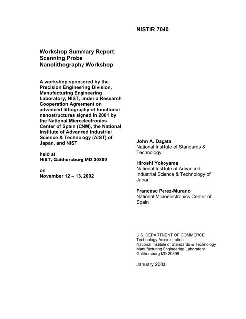
<strong>NIST</strong>IR 7040<strong>Workshop</strong> Summary Report:Scanning Probe<strong>Nanolithography</strong> <strong>Workshop</strong>A workshop sponsored by thePrecision Engineering Division,Manufacturing EngineeringLaboratory, <strong>NIST</strong>, under a ResearchCooperation Agreement onadvanced lithography of functionalnanostructures signed in 2001 bythe <strong>National</strong> MicroelectronicsCenter of Spain (CNM), the <strong>National</strong>Institute of Advanced IndustrialScience & Technology (AIST) ofJapan, and <strong>NIST</strong>.held at<strong>NIST</strong>, Gaithersburg MD 20899onNovember 12 – 13, 2002John A. Dagata<strong>National</strong> Institute of Standards &TechnologyHiroshi Yokoyama<strong>National</strong> Institute of AdvancedIndustrial Science & Technology ofJapanFrancesc Perez-Murano<strong>National</strong> Microelectronics Center ofSpainU.S. DEPARTMENT OF COMMERCETechnology Administration<strong>National</strong> Institute of Standards & TechnologyManufacturing Engineering LaboratoryGaithersburg MD 20899January 2003
EXECUTIVE SUMMARYA workshop on Scanning Probe Microscope (<strong>SPM</strong>)-based <strong>Nanolithography</strong> was held at <strong>NIST</strong>Gaithersburg on November 24-25, 2002. The meeting was sponsored by the PrecisionEngineering Division, Manufacturing Engineering Laboratory, <strong>NIST</strong>, under a ResearchCooperation Agreement on advanced lithography of functional nanostructures signed in 2001 bythe <strong>National</strong> Microelectronics Center of Spain (CNM), the <strong>National</strong> Institute of AdvancedIndustrial Science & Technology (AIST) of Japan, and <strong>NIST</strong>.The workshop program focused on fundamental studies in nanoscience, the kinetics andmodeling of <strong>SPM</strong> oxidation, and applications to nanotechnology, Fundamental studies includeddiscussions of current measurement during <strong>SPM</strong> oxidation, measurement of charge & densityvariation in <strong>SPM</strong> oxides, control & understanding of the meniscus shape, and 3-D multiphysicsmodeling of electrostatics, transport, and chemical reaction during <strong>SPM</strong> oxidation. Applicationsto nanotechnology included the fabrication of nano-electronics, nano-photonics, nanoelectromechanical,and microfluidic devices and systems.ACKNOWLEDGMENTSWe thank Dennis Swyt and Michael Postek of the Precision Engineering Division of <strong>NIST</strong> forproviding financial support for this workshop, Regenia McCloud of the Precision EngineeringDivision for expert assistance in coordinating visitors’ travel plans and conference preparations,and Steve Knight and Jack Martinez of the <strong>NIST</strong> Office of Microelectronic Programs for supportof the nanoscale metrology group’s nanofabrication program.3
ABSTRACTA workshop on Scanning Probe Microscope (<strong>SPM</strong>)-based <strong>Nanolithography</strong> was held at <strong>NIST</strong>Gaithersburg on November 24-25, 2002. The meeting was sponsored by the PrecisionEngineering Division, Manufacturing Engineering Laboratory, <strong>NIST</strong>, under a ResearchCooperation Agreement on advanced lithography of functional nanostructures signed in 2001 bythe <strong>National</strong> Microelectronics Center of Spain (CNM), the <strong>National</strong> Institute of AdvancedIndustrial Science & Technology (AIST) of Japan, and <strong>NIST</strong>. A dozen active collaborators of<strong>NIST</strong>, AIST, and CNM projects in this emerging field presented their most recent results onfundamental aspects of nanostructure fabrication and characterization and on the application of<strong>SPM</strong> nanostructures to nano-electronics, nano-optics, and nano-mechanical devices.5
TABLE OF CONTENTSEXECUTIVE SUMMARY 3ACKNOWLEDGMENTS 3ABSTRACT 6WORKSHOP AGENDA 9EXTENDED ABSTRACTS 15PARTICIPANTS LIST 837
WORKSHOP AGENDA9
<strong>SPM</strong> <strong>Nanolithography</strong> <strong>Workshop</strong>November 12 - 13, 2002<strong>National</strong> Institute of Standards and TechnologyGaithersburg MD 20899 USASponsored by the Precision Engineering Division, Manufacturing Engineering Laboratory, <strong>NIST</strong>,under a Research Cooperation Agreement on advanced lithography of functional nanostructuressigned in 2001 by the <strong>National</strong> Microelectronics Center of Spain (CNM), the <strong>National</strong> Instituteof Advanced Industrial Science & Technology (AIST) of Japan, and <strong>NIST</strong>.Preliminary AgendaTuesday, November 12, 2002Room B-321, Metrology Building (220) NOTE ROOM CHANGE THIS DAY ONLY8:00 - 8:30 A.M.Arrival and check-in8:30 - A.M.Dale Hall, Director of the Manufacturing Engineering Laboratory, <strong>NIST</strong>: Welcome andIntroduction to MEL and <strong>NIST</strong>John Dagata, <strong>NIST</strong>: History and scope of this workshop9:00 - A.M.Hiroshi Yokoyama, AIST: Use of scanning probe nanofabrication for creating liquid-crystalnanostructures9:30 - A.M.Francesc Perez-Murano, CNM: Non-contact AFM nano-oxidation: new experiments andapplication to thin aluminum films10:00 - A.M.Hiromi Kuramochi, AIST: Current detection during Si nano-oxidation10:30 - 11:00 A.MBREAK11:00 - A.M.Felix Gwo, N. Tsing-Hua U (Taiwan): Study of trapped charges in scanning-probe-inducedoxides by electrostatic force microscopy11
11:30 - A.M.Jerry Young, U of Akron: Free boundaries in an electrochemical nanocell12:00 1:00 PMLUNCH (Cafeteria)1:00 - P.M.Takashi Tokizaki, AIST:Application of <strong>SPM</strong> oxidation to nano-photonics and nano-spintronics1:30 - P.M.Rex Ramsier, U of Akron: Nanoscale oxidation of zirconium surfaces: kinetics and mechanism2:00 - P.M.Zach Davis, Danish Tech U (Denmark): Status of the EU NANOMASS Project2:30 - 3:00 P.M.BREAK3:30 - P.M.Forest Chien, ITRI (Taiwan): Fabrication of Si nanostructures by Scanning Probe Oxidation andAnisotropic Wet Etching.4:00 - P.M.Mike Fasolka, <strong>NIST</strong>: Overview of the <strong>NIST</strong> Combinatorial Methods Center4:30 - P.M.Tony Schmitz, U of FL: <strong>Nanolithography</strong> and microfluidics: a manufacturing perspective5:00 - P.M.John Dagata, <strong>NIST</strong>: Integration of <strong>SPM</strong> nanolithography, nanoimprint lithography, andmicrofluidics5:30- 6:00 P.M.DISCUSSION & ADJOURN7:00 - P.M .DINNER (TBD)November 13, 2002Room B-111, Administration Building (101)9:00 A.M.Arrival12
9:15 - 10:30 A.M.Discussion 1Topic: Identifying and measuring experimental input parameters required for quantitativemodeling of transport and reaction processes during <strong>SPM</strong> oxidationFrancesc Perez-Murano & Jerry Young, discussion leaders10:30 - 11:00 A.M.BREAK11:00 A.M. 12:00 P.M.Discussion 2Topic: Prospects for using <strong>SPM</strong> oxidation as a materials characterization techniqueFelix Gwo & Rex Ramsier, discussion leaders12:00 - 1:00 P.M.LUNCH (Cafeteria)1:00 - 2:15 P.M.Discussion 3Topic: Nanostructured templates and self-organized chemistryHiroshi Yokoyama & Mike Fasolka, discussion leaders2:15 - 3:15 P.M.BREAK3:15 - 4:30Discussion 4Topic:Designs and timelines for nanofluidic, photonic, and NEMS devicesZach Davis & Forest Chien, discussion leaders4:30 P.M .ADJOURN13
EXTENDED ABSTRACTS15
Welcome to the Manufacturing Engineering Laboratory at the<strong>National</strong> Institute of Standards and TechnologyDale Hall, Director, Manufacturing Engineering Laboratory (MEL)<strong>NIST</strong> has a long history of involvement with scanning probe microscopy, from the pioneeringwork of Russell Young in the 1970’s, to its advancement as a metrology tool by Clayton Teaguein the 1980’s & 1990’s. Since 1990, we’ve continued our scientific advancements innanolithography and nanofabrication.<strong>NIST</strong> and MEL serve established industries, such as automotive and semiconductor, as well asnascent industries such a biotechnology and nanotechnology. Let me give you some backgroundon <strong>NIST</strong>. <strong>NIST</strong>’s predecessor - the <strong>National</strong> Bureau of Standards, was established in 1901. In1988, Congress assigned several new and major responsibilities to the organization and renamedthe agency the <strong>National</strong> Institute of Standards and Technology. <strong>NIST</strong> is part of the U.S.Department of Commerce and its mission is to strengthen the U.S. economy and improve thequality of life by working with industry to develop and apply technology, measurements, andstandards. We carry out this mission through a portfolio of four major programs:• The Advanced Technology Partnership program is a unique co-funded partnershipbetween <strong>NIST</strong> and private industry to accelerate the development of high-risk, enablingtechnologies with broad benefits for the entire economy and for society.• The Manufacturing Extension Partnership program is a nationwide network of locallymanaged extension centers offering technical assistance and best business practices to theNation’s 385,000 smaller manufacturers in all 50 states, DC and Puerto Rico.• The Malcolm Baldridge <strong>National</strong> Quality Program is an outreach program that recognizesU.S. manufacturing, service, education, and health care organizations for theirachievements in quality and performance and to raise awareness about the importance ofquality and performance excellence as a competitive edge.• The <strong>NIST</strong> measurement and science laboratories are the Nation’s ultimate reference pointfor measurements, standards, and metrology research to support industry, science, health,safety and the environment.<strong>NIST</strong> maintains the U.S. national standards for all fundamental measurements (length, time,mass, electric current, etc.) and for dozens of derived measurements. The staff works withindustry on measurement (methods, evaluated data, and test procedures) and standard issues.The U.S. economy depends upon <strong>NIST</strong> measurements. <strong>NIST</strong> measurements are used to makesure that our everyday life functions smoothly. For example, telecommunication devices,computer chips, pharmaceuticals, medical imaging, even gas pumps, rely on fundamentalmeasurements to ensure proper operations.<strong>NIST</strong> has seven technical laboratories: Physics, Information Technology, Electronics andElectrical Engineering, Materials Science and Engineering, Chemical Science and Technology,Building and Fire Research, and my own lab –Manufacturing Engineering.17
The laboratory programs cover a broad range of subjects and much of our work ismultidisciplinary, with collaboration among the labs. The major U.S. effort in nanotechnologyrequires the kind of inter-laboratory and multidisciplinary collaboration that is in many instancesunique to the <strong>NIST</strong> laboratories.Nanotechnology is the creation and utilization of materials, devices, and systems through thecontrol of matter on the nanometer-length scale, that is, at the level of atoms, molecules, andsupra-molecular structures. The U.S. <strong>National</strong> Nanotechnology Initiative (NNI) has spurredintense interest on the part of other nations and regions to begin programs of their own. Withinthe NNI, <strong>NIST</strong>’s involvement is in the development of measurement technologies and standardsto assist U.S. industry at the nanometer-scale level. Although it is too early to know exactlywhen and how the critical components of nanotechnology will impact industrial products andservices, it is crucial for <strong>NIST</strong> labs to gain the expertise required to provide measurements andstandards at the nanoscale as demanded by industry. Our efforts are now focused on putting thisinfrastructure into place.This infrastructure will help <strong>NIST</strong> support opportunities to commercialize nanotechnology in theU.S. and facilitate international trade. <strong>NIST</strong> enables commercialization and international tradethrough: a) nanoscale measurement science, and b) nanoscale measurement standards.The NNI issued several “Grand Challenges” some of which directed specifically to U.S.government agencies to help them identify and begin working on the support infrastructureneeded for commercializing nanotechnology. To build that infrastructure, we need to explore: a)New measurement tools and techniques - basic science needed; b) Facilities – uniqueinstrumentation and specially designed measurements labs; and c) Standards and traceability fornanotechnology.Some examples of the technical challenges that we have are issues with: a) resolution -molecular to atomic spatial scales and high-speed temporal scales; b) sensitivity and specificity -i.e., molecular or atomic level sensitivity and specificity with simultaneous imaging andidentification, and simultaneous multiple spectroscopy for chemical and physical properties, c)3-D characterization capability, and 4) automated databases.Within the U. S., MEL has primary responsibility for length- and mass-based standards. MEL’slength-based measurements range from 100’s of meters to picometers. The instruments that weuse for dimensional metrology includes laser trackers, coordinate measuring machines, opticalinterferometers, scanning electron-beam microscopes, and -- of particular interest to you --scanning probe microscopes.There are many ways to describe the type of work that MEL does. I’ve chosen to describe ourtechnical agenda using four main themes: Measurements and Standards for Making Things…a)Right, b) Interoperable, c) Traceable, and d) Small. All of our programs can be mapped intothese themes. While the connection between MEL’s technical theme of “Making Things Small”and the some of the NNI Grand Challenges are obvious, I do want to stress that, from themanufacturing perspective, many of the novel fabrication processes and measurement18
technologies that make nanodevices and nanosystems feasible must evolve under the samerequirements to which all successful manufacturing must conform - hardware and softwareelements of these devices and systems must be made … right, interoperable, and traceable, notonly small.It is amazing to thing that over four decades ago, Richard P. Feynman predicted the coming ofthe nanotechnology age in his famous talk “There’s Plenty of Room at the Bottom”.Nanotechnology will transform many of the technical devices as we know them, however, beforewe can get there, scientists need to perfect positional control at the atomic level and to keep thecost down, there needs to be a reliable and probably self replication manufacturing system. Youneed to be able to build a small basic unit at the atom level and then combine units to create thelarger product.While it is clear that nanotechnology will revolutionize many industries, for practical realizationof nanotechnology, we must be able to measure nanoscale properties accurately andreproducibly. <strong>NIST</strong> helps build the measurement infrastructure to support the development andapplication of nanotechnology. MEL’s metrology research encompasses optical, electron, andprobe-based metrology. Here are some examples of our work. Optical instruments are used tocalibrate and develop measurements and standards for pitch and linewidth used in manyindustries. Photomask overlay metrology is important for the semiconductor industry. Modelbasedscanning electron-beam (SEM) metrology meets another a critical need of thesemiconductor industry. Model-based SEM metrology methods developed here show that thetechnique is comparable to the traditional but more expensive destructive cross sectionaltechnique. These differences are within the uncertainty attributable to line edge roughness.Within MEL, we have three unique scanning probe microscope systems that we use fordimensional metrology research. The Molecular Measuring Machine features a scanningtunneling microscope with a Michelson interferometry. Our goal is to maintain nanometeruncertainty for point-to-point measurements within the 50 mm x 50 mm measurement area. TheCalibrated Atomic Force Microscope (C-AFM) is used to calibrate tools for measurements ofsurface structures or surface roughness where the measured height parameter is less than 1 nm.The C-AFM is used primarily for <strong>NIST</strong> measurements of the Si(111) single atom step height butcan also be used to perform linewidth measurements in an intercomparison of differentmeasurement techniques. The UHV STM/FIM (ultrahigh vacuum scanning tunnelingmicroscope/field-ion microscope) is really a facility or system because it contains multiple UHVchambers: one for very leading-edge sample preparation, one for the FIM – used to accuratelycharacterize at the atomic-level tip shapes, and the last for the STM - the tips characterized in theFIM are used in this chamber to measure and prepare atomically ordered substrates. The sampleand tips used for measurements are prepared to atomically precise conditions in ultra-highvacuum (UHV) portion of the system. The system has a tunable diode laser-based, frequencytrackinginterferometer with picometer resolution. With this system, we can measure atomspacingsdirectly rather than using the conventional fringe counting. Our current research islooking for ways to make samples in a reproducible manner anywhere from the 10 nm down tothe atomic dimension level.19
MEL is also exploring novel fabrication methods for nanostructures. Let me give you someexamples of our own efforts to prototype nanoscale standards. The first example is a pitchcalibration prototype designed and prepared here at <strong>NIST</strong> by scanning probe lithography andsilicon etching. These prototypes demonstrate that 100-nm minimum pitch and sub-50-nmlinewidth can be obtained. Pitch placement accuracy has been analyzed using statistical methodsdeveloped in the optical and SEM dimensional metrology projects. This work was performed incollaboration with a guest researcher from the Center for Measurement Standards in Taiwan,Forest Chien. Another example is a replica of a magnification artifact produced by the 'softlithography' technique (casting a silicon mold using poly dimethyl siloxane, or PDMS). Sinceone of the manufacturing goals of nanotechnology is low unit-cost production, there is a greatneed for, and growing interest in, commercializing rapid and cheap prototyping methods.<strong>NIST</strong> partners with industrial consortia, individual companies, other government agencies, anduniversities. When <strong>NIST</strong> works on a technical issue with its partners, we tend to focus on issuesthat can benefit industry sectors in a broad sense. Our partnerships typically relate tomeasurements and standards issues. I would like to encourage further interactions among all ofthe workshop participants.Successfully bringing nanotechnology to industry will depend on meeting challenges inmeasurement, fundamental understanding, and control of dimensional and materials propertiesand processes that work at the nanometer level. Length, height, force, tribology, finish, andcomposition are just a few of the properties that we must deal with simultaneously in order thatcomponents of nanoscale devices and systems are made “right, interoperable, traceable, as wellas small.” I encourage you to ask questions and follow up on any of our work that you findinteresting. Descriptions of <strong>NIST</strong>’s or MEL’s technical programs can be found on website –www.nist.gov.20
<strong>SPM</strong> <strong>Nanolithography</strong> <strong>Workshop</strong><strong>National</strong> Institute of Standards and TechnologyNovember 12-13, 2002History and scope of this workshopJohn A. DagataPrecision Engineering DivisionManufacturing Engineering Laboratory<strong>National</strong> Institute of Standards and TechnologyGaithersburg MD 20899 USAHistory of this workshopIt is worth recording briefly how this workshop on scanning probe microscope (<strong>SPM</strong>)-basednanolithography evolved. New opportunities for US government scientists to collaborate directlywith their counterparts in the Japanese government arose through the signing of the US-JapanFramework Agreement of 1993-1994. In particular, this agreement simplified processes forestablishing collaboration between <strong>NIST</strong> and MITI’s Agency of Industrial Science &Technology (AIST). This prompted discussions in 1996 between myself and Hiroshi Yokoyamaand Junji Itoh of AIST’s Electrotechnical Laboratory (ETL) on the possibility of establishingregular research visits aimed at integrating scanning probe lithography and electric forcemicroscopy (EFM) for nanodevice applications. <strong>SPM</strong> oxidation, as everyone at this workshopknows, was a technique first demonstrated at <strong>NIST</strong> in 1990. The scanning Maxwell-stressapproach to EFM was likewise formulated by Drs. Yokoyama and Itoh in 1992 at ETL. My firstresearch visit to ETL occurred during Dec 1996-Jan 1997.During that visit we initiated two experimentaldirections which figure prominently in the range oftopics that will be discussed at the present workshop.First, working with Alamgir Karim of the PolymersDivision at <strong>NIST</strong>, we prepared thin-film samples of aconducting polymer, polythiophene, blended withpolystyrene as a test system for subsurface EFMimaging. Because of the dielectric difference betweenthese two organic components, we were able to observethe inhomogeneous distribution of the components inseparated phases and follow subsurface annealingdependentreorganization for film thicknesses up to 100nm. A21Figure 1
visualization of the subsurface polythiophene network near the silicon substrate within thepolystyrene-rich phase appears in Figure 1. Materials characterization using EFM in combinationwith other <strong>SPM</strong> methods remains one of foundational approaches of our research.Second, we demonstrated the feasibilityof producing <strong>SPM</strong> oxide features -- sub-100-nm dots on silicon substrates, forexample -- and then using EFM to imagethe potential signature of these features.This research indicated that dopingdependenttrapped charge was presentwithin the silicon oxide and thereforeshould tell us something about theunderlying kinetics and mechanism ofthe oxidation reaction. Application ofthis integrated approach led to designand fabrication of a silicon device incollaboration with Kiyoshi Morimoto(Matsushita) as part of his involvementin MITI’s Quantum Functional Devicesproject. Figure 2 illustrates the integratedsystem for <strong>SPM</strong> lithography, EFMimaging, with simultaneous currentvoltage(I-V) device measurementcapabilities along with the device. Dr.Morimoto spent 3 months as a visitingresearcher at <strong>NIST</strong> in 1999 analyzinghigh-resolution cross-sectionaltransmission electron microscope resultsand drafting a manuscript. Internal I-Vtesting of the device has been comparedwith local EFM imaging to locateregions of inhomogeneous trappedcharge at the buried Si/SiO 2 interface.In 1997, Francesc Perez-Murano of theUniv. Autonoma Barcelona and I begancollaboration with the intention ofaligning the <strong>NIST</strong>-ETL integrated-oxidecharacterization effort with UAB’sstudies of the meniscus control madepossible by <strong>SPM</strong> oxidation performed indynamic mode. This collaboration wasinitially supported in part by a FulbrightCommission grant for US-SpainIntegrated probe station andscanned probe microscopedeviceelectrical probes65nm p ++ -Si105n Buried (S )Figure 2222μ<strong>SPM</strong> tipMetalp ++ -SiThinned p ++ -Si areaSubstrate (backgate)CVDSiO 2
Cooperative Research. Publication of voltage modulation, density variation, and space-chargemodeling studies of <strong>SPM</strong> oxidation were an outcome of this collaboration.After having met in Japan, Europe, and the US at various meetings and workshops 1 , it becameapparent to Hiroshi, Francesc, and I that a more formal agreement would facilitate regularexchange of information, help each of us to focus on new directions, and help to broaden ourproductive and ongoing discussions to include a wider circle of collaborators. In September 2001a Cooperative Research Agreement was signed by CNM of Spain, AIST of Japan, and <strong>NIST</strong> topromote advanced lithography of nanostructures and we agreed to hold this next workshop at<strong>NIST</strong>.Scope of this workshopThe organization of this workshop follows a somewhat arbitrary distinction betweenfundamental studies in nanoscience – the kinetics and modeling of <strong>SPM</strong> oxidation -- andapplications to nanotechnology, particularly fabrication of nano-electronics, nano-photonics, andnano-electromechanical devices and systems. Fundamental studies that promise to lead to a morecomplete understanding, predication, and application of <strong>SPM</strong> oxidation are covered in thefollowing talks:• Current measurement during <strong>SPM</strong> oxidation (Francesc Perez-Murano, HiromiKuramochi)• Measurement of charge & density variation in <strong>SPM</strong> oxides (Felix Gwo)• Control & understanding of the meniscus shape (Francesc Perez-Murano)• 3-D multiphysics modeling of electrostatics, transport, and chemical reactions (JerryYoung).Hiroshi has long argued that reliable current measurements during <strong>SPM</strong> oxidation are required tocomplement our earlier EFM measurements of the resulting oxide charge and volume to gaincomplete understanding and control of the process. The measurements that Francesc and HiromiKuramochi (AIST) have made recently are extremely promising in this regard. These effortsrepresent essential input into the modeling efforts of Jerry Young and his colleagues at the Univ.of Akron in bringing a self-consistent method to solving the system of reaction-diffusionequations. These equations describe the chemical aspects of oxide film growth with the physicaldescription of the electrostatic field that exists within the water meniscus and its dielectric/ioniccharacter during exposure. The extent to which it is becoming possible to control the meniscusshape, and thereby the total current passing through the system, as Francesc discusses in hispresentation, must be accounted for within the model. The composition of the resulting oxide1 SP-Nano I - Tsukuba 1997, QFD Society Meeting - Gaithersburg 1997, SP-Nano II - Tsukuba1999, Informal workshop on <strong>SPM</strong> lithography - Tsukuba 2000, Limits to miniaturization -Barcelona 2002, <strong>SPM</strong> <strong>Nanolithography</strong> workshop - Gaithersburg 2002.23
film must reflect the fact that considerable charge may be present within <strong>SPM</strong> oxide, a result firstpointed out in the initial experiments that Hiroshi and I performed in 1996-7. In addition, asatisfactory model must account for the lower density of the oxide and its variability withexposure conditions, as discussed in the papers that Francesc, Dr. Morimoto, and I co-authoredin recent years.Since then, Felix Gwo and his group at <strong>National</strong> Tsing-hua Univ. have adopted a strategy ofusing in-situ EFM to gain detailed understanding of charge trapping within silicon and siliconnitride films. Using a low-vacuum system for environment and temperature control, they haveperformed systematic identification of electronic and ionic species and lifetimes. Sustainedprogress will provide essential input and consistency checks on emerging models.Applications to nanotechnology are described in the following talks:• Materials characterization (Felix Gwo, Rex Ramsier)• Nanoelectronic devices (Takashi Tokizaki)• Nanoelectromechanical systems (Zach Davis)• Optics and photonics (Hiroshi Yokoyama, Forest Chien, Takashi Tokizaki)• Microfluidic systems (Tony Schmitz, Mike Fasolka)A basic tenet of nanotechnology – at least in my view – is that fabrication and characterizationbecome inextricably intertwined at the nanoscale. Prototyping efforts that provide value-addedinformation about dimensional and materials properties are a unique aspect of <strong>SPM</strong> methods.Felix extends the use of EFM to characterization of charge deposited within oxide and nitridefilms for data storage. Similarly, Rex Ramsier and his group are applying <strong>SPM</strong> oxide growthkinetics to augment their surface science studies of Zr and ZrN thin films. A significant portionof the data for Zr and ZrN thin films was obtained by Natalia Farkas, a graduate student at Univof Akron, during a 6-week research visit to <strong>NIST</strong> in 2001. Of particular interest are the rich andcomplicated chemical reactions between surface and subsurface oxygen, nitrogen, and hydrogenspecies that they have catalogued using thermal and e-beam activation. Coupled with Felix’sevidence for complete conversion of Si 3 N 4 to SiO x by <strong>SPM</strong> oxidation, it will be very satisfyingto understand the details of the corresponding conversion in the ZrN system.A compelling aspect of <strong>SPM</strong> oxidation is that almost every material oxidizes under the extremeelectric-field conditions that exist between the tip and substrate during <strong>SPM</strong> oxidation. Examplesof <strong>SPM</strong> oxide patterning of device-related materials that have appeared in the literature recentlyinclude diamond, superconducting materials, magnetic, and 2-D electron gas in III-Vsemiconductors. Spintronic devices are being studied with great interest currently and TakashiTokizaki (AIST) reports on his efforts to pattern such materials. Zach Davis (Danish Tech.Univ.) provides a status report on fabricating a nanomechanical resonator using <strong>SPM</strong> oxidation.<strong>SPM</strong> oxidation is combined with laser lithography of an aluminum film to pattern the mask24
defining the resonator structure by reactive ion etching. A key aspect of this joint researchactivity between the Danish Microelectronic Center and the <strong>National</strong> Microelectronics Center ofSpain is that the processing sequence is integrated with standard CMOS technology. This work isbeing funded under a European Union research grant now in Phase II.Optics and photonics applications of <strong>SPM</strong> lithography are underway and a number of ideas anddirections will be presented. Hiroshi is also the leader of an ERATO project in Japan and in thisrole discusses the use of <strong>SPM</strong> lithography for patterning liquid-crystals with elegant control ofdomains at the sub-micrometer scale. Forest Chien of the Industrial Technology ResearchInstitute of Taiwan discusses fabrication of 2-D silicon nanoarrays using <strong>SPM</strong> oxidation andanisotropic wet etching for potential use as photonic crystals. Forest spent 6 months as a visitingresearcher at <strong>NIST</strong> extending his PhD-thesis work on KOH etching to tetra-methyl ammoniumhydroxide etchants and Si(100) and silicon-on-insulator (SOI) substrates, providing a significantdatabase for the optimum production of sub-micrometer silicon nanostructures. Takashi Tokizakialso reviews his unique work using an Al-coated near-field scanning optical microscope(NSOM) tip to simultaneously perform <strong>SPM</strong> oxidation of a sub-wavelength optical waveguideand measure the resulting optical transmission characteristics.Finally, Mike Fasolka (<strong>NIST</strong>) describes the mission and capabilities of the <strong>NIST</strong> CombinatorialMethods Center. During the past year Mike and I have identified several opportunities forcombining dimensional and chemical patterning with the gradient methods being developed bythe Center. In his presentation, Tony Schmitz (Univ. of FL) summarizes our collaboration duringthe past year aimed at gaining basic expertise in microfluidic device fabrication and nanoimprintlithography using hot embossing techniques. Our initial results suggest that microfluidic devicesprovide a significant platform for incorporating <strong>SPM</strong>-fabricated nanostructures in the near future.25
Tri-stable nematic liquid-crystal device using orientationallyfrustrated surface patterns fabricated by the atomic forcemicroscopy nanorubbingHiroshi Yokoyama* † , Jong-Hyun Kim* and Makoto Yoneya** Yokoyama Nano-structured Liquid Crystal Project, ERATO, Japan Science and TechnologyCorporation, TRC 5-9-9 Tokodai, Tsukuba, Ibaraki 300-2635, Japan, † Nanotechnology ResearchInstitute, <strong>National</strong> Institute of Advanced Industrial Science and Technology 1-1-1 Umezono,Tsukuba, Ibaraki 305-8568, JapanMulti-stable liquid-crystal (LC) devices are known for many years to be desirable forrealizing drastically reduced power consumption needed for high information contentmobile displays. However, no industrially feasible multi-stable nematic liquid-crystal(NLC) device has ever been realized due to their inherent uniaxial symmetry 1-7 . Recentlywe demonstrated a robust surface-alignment bistability on micro-fabricated orientationalcheckerboard pattern, in which neighbouring unit square domains are so treated as toenforce mutually orthogonal alignment 8,9 . The four-fold symmetry of the patternautomatically allowed the two diagonal axes of the checkerboard to become equally stablemacroscopic orientations. Here we report the first tri-stable surface alignment of NLCstailored by extending the symmetry approach. A six-fold symmetrical orientational micropattern was inscribed on polyimide surface by nano-rubbing using the stylus of atomicforce microscope (AFM). The surface is tiled with 60-degree rotated nano-rubbedparallelograms. The hexagonal symmetry ensures the three local rubbing directions to givestable macroscopic LC orientations in the bulk, which are mutually switchable by an inplaneelectric field. The new LC mode is surface-driven and hence essentially compatiblewith ever demanding flexible display applications. The present result also illustrates how ananotechnology tool can be useful in prototyping a cutting edge LC device.It has long been known that, on a fresh surface of a cleaved single crystal such as NaCl,mica, etc., NLCs can assume multiply stable orientations, faithfully reflecting thecrystallographic axes 10-12 . Given the microscopic uniformity of the cleavage surface, the ordinaryanchoring energy coefficient, which is generally represented by a second rank tensor 1 , should beisotropic for surfaces with four-fold or higher-order symmetries. This implies that the multistabilityobserved on single crystal surfaces is a higher-order anchoring effect that makes itsusceptible to external contaminants and disturbances leading to the first-order anchoringeffect 13 .Borrowing the concept of symmetry on single crystals while retaining the first-orderrobustness of our frustrated micro-patterning, we devised a higher symmetry surface patterns to27
ealize artificial multi-stability of NLCs. As an example of this approach, we demonstrate here atri-stability on a hexagonally symmetric pattern consisting of locally rubbed parallelograms asshown in Fig.1. The shape of the parallelogram was designed to have the corner angles of 60°and 120 ° so that three of them, mutually rotated by ± 60 ° , make a hexagon. The infinitelyextended pattern tiled with the hexagons (Fig1a) has a six-fold rotational symmetry.For the purpose of examining the aligning characteristics of the orientational pattern, wefabricated a structure comprised of unit domains as large as 10μm (Fig.1b). We carried out thenano-rubbing on a polyimide-coated glass slide 14-17 , the details of which have been describedelsewhere 8,9,17 . In brief, the precursory polyamic acid (SE-150, Nissan Chemical Co.) was spunon the glass slide and was baked. For the nano-rubbing, an AFM ( SPA-500, Seiko InstrumentsInc.) was used in the contact mode. The nano-rubbed polyimide surface acquired the ability toalign LC in parallel to the surface along the symmetrically scanned direction, giving a zero tiltbias angle 17 . A room temperature NLC, 4-n-pentyl-4’-cyanobiphenyl (5CB), was applied ontothe patterned surface to an appropriate thickness without a cover slide.Since the size of the unit domain is large here, LC orientations on individual domains andat the domain boundaries are clearly resolved in the micrographs (Fig1b). The contrast changesunder a rotating analyzer confirm that the alignment inside the unit domain is along the localrubbing direction. The domain boundaries also have a distinct brightness, reflecting thealignment transition from one domain to the next. As indicated by the director symbols in Fig1c,two of the three boundaries meeting at a corner are associated with 60° in-plane rotation fromone domain to the next (π/3-wall), whereas the remaining one is associated with 120° rotation(2π/3-wall). This combination of walls corresponds to the lowest free-energy configuration thatcan cover the entire surface without introduction of point defects. Depending on the position ofthe 2π/3-wall boundary, there appear three orientationally distinct, yet energetically equivalentstates as depicted in Fig.2. These states are mutually convertible by way of 180° rotation of thedirector in an appropriate one of the three constituent parallelograms, and are the basis of thepresent tri-stability. The global configuration of the director for a given surface orientation isdetermined in such a way as to minimize orientational distortions described by the Frank elasticenergy18 . Consequently, the inhomogeneous LC orientation imposed by the patterned surfacerelaxes rapidly into a uniform bulk alignment, which bears three stable axes depending on therelative arrangement of π/3- and 2π/3-walls. More quantitatively, if we assume the one-constantapproximation, the equilibrium configuration of the director azimuth φ satisfies the Laplace18equation Δ φ = 0 . It follows that the laterally inhomogeneous component of φ with the wavevector k decays exponentially as exp( − k z)with the distance z along the surface normal intothe bulk LC. Therefore, the director profile at a point away from the surface by a distance largerthan the unit domain size d becomes virtually uniform with the orientation φ ( z ) = φ(0), wheredenotes the average over the surface. This shows that one stable bulk orientation is identicalwith the local orientation on the unit domain located between the two π/3-walls. The remainingtwo stable states are generated from this configuration by the natural symmetry operation of28
NLCs to flip the surface director by 180°giving rise to a 60 ° shift of φ (0).over any particular subset of parallelograms (Fig.2),To confirm the tri-stabile alignment, the hexagonal pattern was scaled down to the quarterof the aforementioned pattern to be of 2.4μm side length. As the size of the unit domainapproaches the wavelength of visible light, the optical uniformity of the patterned area rapidlyimproves for the decrease of the orientational relaxation length 1 / k and the increase of theoptical diffraction angle beyond the numerical aperture of the observation optics. By combiningthe patterned substrate with a counter polyimide-coated glass slide that was conventionallyrubbed, a 50μm –thick sandwich-type LC cell was fabricated (Fig3a). On the glass substrate alsofabricated were three pair of electrodes to apply in-plane electric fields, concentrically arrangedwith 60° shift as shown in Fig3a. The AFM nano-rubbing was conducted in the central spacebetween electrodes. Nano-rubbing directions were set parallel with the electric field directions.The vacant cell was injected with the NLC. Sinusoidal electric field of 1kHz was used forelectro-optical switching experiments.As shown in Figs.3b and 3c, the hexagonally patterned area clearly showed three stablestates that were mutually switchable by the electric field. The stable states were found resistantto mechanical disturbances for no-disruption of alignment in prolonged experimentation. Thisappears reasonable in that the effective anchoring energy of the tri-stable cell is reduced only by1/3 of a uniform cell, because the switching is associated with the flip of local director on 1/3 ofthe unit parallelograms. As the field is increased along the destination direction, the LC in bulkstarts to reorient along the field. Up to a certain threshold field ≈ 6V / μm, the alignment relaxesback to the original state as the field is turned off. When the field strength exceeds the thresholdfield, the switching begins locally by the domain nucleation and growth. Due to variousinhomogeneities associated with LC injection, non-uniform electric and director fielddistributions on the pattern boundary, the switching cannot be ideally abrupt, but the field shouldbe a little increased before the entire area is switched. While the three different states switchedreversibly between each other, the field strength necessary to drive the a-a’ switching was foundto be larger than those for others (b-b’ and c-c’). The difference might reflect the persistent effectof flow alignment during LC injection 19 , which took place nearly perpendicular to the a-a’. Theoptical transmission measurements revealed that the contrast ratio was about 5 for all states(Fig3c). This ratio has been improved to ca. 20 for a tri-stable device with 1.2μm unit domain.The angle differences between the stable states were not exactly 60 ° , but they were about 50°symmetrically about the LC injection direction.The switching behaviour can be readily analyzed for the extreme cases of small and largeunit domains relative to the anchoring extrapolation length d e = K 22 /W0; here, K22and W0are thetwist elastic constant and anchoring energy, respectively. In the limit of small unit domainsd > d e, on the other hand, we can treat the29
system as a uniform planar structure subjected to an in-plain field and obtain the threshold fieldas Eth = CMW0 / 2 K22Δε for Rapini-Papoular anchoring 1 . Δ ε is the dielectric anisotropy andC = + 21 3M1 3cos ( 2arctan(tan φ −φe E)) is a symmetry factor depending on the relativeazimuthal angle of the field φ Eand the easy direction on the parallelogram φ e. For the tristabilityφe−φ E= 60°, one obtains CM≅ 1. 05 , which shows that the threshold field remainsonly 5% higher than that for the bistability. The observed Eth~ 6V/ μmis consistent with this-4 2estimate, given Eth~ 5V/ μmand W0 ≈ 10 J/m for the bistability8 . It follows that the angle,3± arctan ( tan1 | φ | e− φE), by which the surface director should rotate before the switching slightlyincreases from 45 ° (bistability) to 50.2°(tri-stability).As in the ordinary NLC devices, the cell thickness is a critical parameter determining theelectro-optic response. Due to the patterned nature of the tri-stable surface, there appears a lowerbound for the cell thickness d t, set by the condition that the surface inhomogeneity shouldsufficiently relax inside the cell, i.e., d t>> d / 2π , to give uniform LC alignment to assurequasi-homogeneous optical and elastic behaviours. Only under this condition, the surfaceswitching can be initiated by the in-plane Freedericksz transition in bulk as required by theswitching mechanism 8 . For a domain size of d ≈ 1μm, one may safely adopt a thicknessdt≈ 5μm , indicating that the response speed of the tri-stable device can at least be comparablewith that of existing NLC devices. The thickness dt≈ 50μmused in the present study isobviously an overly safe choice, solely taken for demonstration purposes.In conclusion, we demonstrated for the first time the orientational tri-stability, which couldbe switched by an in-plane electric field. The present approach is believed to be generic, basedonly on the frustration of the periodically aligned LC, not relying on any delicate balance ofmulti-directional forces, and may be extendable to even higher degree of stabilities.Consequently, the property of the tri-stability is not sensitive to the material or fabricationparameters. The anisotropic LC properties coupled with the symmetry of the substrate will openup a rich new area of electro-optical applications and interfacial sciences of liquid crystals.References1. Yokoyama, H. in Handbook of Liquid Crystal Research (ed. Collings, P. J. & Patel, J. S.) Ch.6 (Oxford Univ. Press, New York, 1997).2. Boyd, G. D, Cheng, J. & Ngo, P. D. T. Liquid-crystal orientational bistability and nematicstorage effects. Appl. Phys. Lett. 36, 556-558 (1980).3. Berreman, D. W. & Heffner, W. R. New bistable liquid-crystal twist cell. J. Appl. Phys. 52,3032-3039 (1981).4. Scheffer, T. J. & Nehring, J. A new, highly multiplexable liquid crystal display. Appl. Phys.Lett. 22, 1021-1023 (1984).30
5. Yang, K. H. Weak boundary storage effect in homogeneous liquid crystal cells. Jpn. J. Appl.Phys. 22, 389-393 (1983).6. Ong, H., Meyer, R. B. & Hurd, A. J. Multistable orientation in a nematic liquid-crystal cellinduced by external-field and interfacial interaction. J. Appl. Phys. 55, 2809-2815 (1984).7. Barberi, R., Boix, M. & Durand, G. Electrically controlled surface bistability in nematic liquidcrystals. Appl. Phys. Lett. 55, 2506-2508 (1989).8. Kim, J. H., Yoneya, M., Yamamoto, J. & Yokoyama, H. Surface alignment bistability ofnematic liquid crystals by orientationally frustrated surface patterns. Appl. Phys. Lett. 78, 3055-3057 (2001).9. Kim, J. H., Yoneya, M., Yamamoto, J. & Yokoyama, H. Controlling surface alignment onnanoscopically tailored competing domains. Mol. Cryst. Liq. Cryst. 367, 151-158 (2001).10. Blinov, L. M. & Sonin, A. A. The interaction of nematic liquid crystals with anisotropicsubstrates. Mol. Cryst. Liq. Cryst. 179, 13-25 (1990).11. Schuddeboom, P. C. & Jerome, B. Azimuthal anchoring of liquid crystals on surfaces withhigh symmetry. Phys. Rev. E. 56, 4294-4305 (1997).12. Schuddeboom, P. C. & Jerome, B. Multistable bulk orientation induced by highly symmetricliquid-crystal monolayer. Europhys. Lett. 39, 515-520 (1997).13. Yoneya, M., Kim, J. H. & Yokoyama, H. Simple model for patterned bidirectional anchoringof nematic liquid crystal and its bistability. Appl. Phys. Lett. 80, 374-376 (2002).14. Ruestschim, M., Grutter, P., Funfschilling, J. & Guntherodt, H. J. Creation of liquid crystalwaveguides with scanning force microscopy. Science, 265, 512-514 (1994).15. Pidduck, A. J., Haslam, S. D., Bryan-Brown, G. P., Bannister, R. & Kitely, I. D. Control ofliquid crystal alignment by polyimide surface modification using atomic force microscopy. Appl.Phys. Lett. 71, 2907-2909 (1997).16. Rastegar, A., Skarabot, M., Blij, B. & Rasing, Th. Mechanism of liquid crystal alignment onsubmicron patterned surfaces. J. Appl. Phys. 89, 960-964 (2001).17. Kim, J. H., Yoneya, M., Yamamoto, J. & Yokoyama, H. Nano-rubbing of a liquid crystalalignment layer by an atomic force microscope: a detailed characterization. Nanotechnology 13,133-137 (2002).18. de Gennes, P. G. & Prost, J. The Physics of Liquid Crystals, (Oxford Univ. Press, New York,1993).19. Yamaguchi, R. & Sato, S. Determination of nematic liquid crystal (NLC) orientation byobserving NLC droplets on alignment surfaces. Jpn. J. Appl. Phys. 35, L117-L119 (1996).31
abcFigure 1. Schematic diagram of the alignment pattern and texture of NLC on the surface. (a) Thepattern is an array of identical hexagons, which consist of three elemental parallelograms. Eachparallelogram has a shifted local rubbing direction, which is expressed by the solid lines. (b) TheLC texture on the patterned alignment layer under a rotating analyzer in the optical polarizing microscope.Outside of the patterned area was left as-coated. The slight contrast of brightness in the figure indicatesthat the patterned region is divided globally into two regions of different macroscopic orientations. Blackand white arrows indicate the directions of polarizer and analyzer. The side of the unit parallelogram is10μm-long. (c) Orientations of surface directors in individual domains and at boundaries. Greenarrows indicate the macroscopic orientations of two regions. Blue ‘T’ symbols correspond to the directorinside the domains and at the boundaries associated with 60 ° in-plane twist (π/3-wall). Red ‘T’ symbolsare the directors at the 120 ° in-plane twist boundaries (2π/3-wall).32
Averageorientation60 0 degree-600-1200-60-60 degree60012060 degreeFigure 2. Three possible macroscopic orientations of NLC on the hexagonal pattern. The lines inside thepattern indicate the local rubbing direction, in which the LC is locally aligned. The NLC and localrubbing are invariant to 180 ° rotation. The three types of hexagons on the right illustrate theenergetically degenerate ground states, which differ from each other in terms of the position of the 120°in-plane twist boundary. Starting from any one of the hexagons, the LC orientations on the remaining twotypes of hexagons can be obtained by flipping the director by 180 ° in one of the three unitparallelograms. The macroscopic LC alignment, appearing sufficiently inside the bulk LC, is simply givenby averaging the director orientation over the surface, and is 0 ° , − 60 ° and + 60 ° from top to bottom.Thick blue and red lines show the π/3- and 2π/3-walls, respectively. Black arrows are the macroscopic LCalignment orientations. The exact match between the macroscopic alignment and either one of the localrubbing directions is valid only when the elastic anisotropy is negligible and/or the inscribed pattern is notchiral. The present hexagonal pattern is chiral in the sense that its mirror image cannot overlap itself. Ingeneral, therefore, the macroscopic alignment could be slightly shifted from the local rubbing direction,although the 60 ° difference among three stable states remains the same owing to its symmetry origin.33
abθElectricFielda-a’ b-b` c-c’-20Anab’ c’a’ a30cbPol80Intensity (a.u.)2418126c-90 -45 0 45 90θ(degree)Figure 3. Structure of the LC cell and tri-stable switching behaviours. (a) The size of thepattern was about 90μm by 90μm. The in-plane electric field was applied along a-a’, b-b’, and c-c’ forswitching. The cell was placed under a polarizing optical microscope for texture observations and forlight transmission measurements. Conventional rubbing on the covering substrate and the polarizerwere set parallel to each other, and one of the local nano-rubbing was adjusted perpendicular to it. Theθ is the angle of the analyzer from the crossed analyzer direction. (b) The LC textures of theswitched states in the absence of electric field; the applied electric field was : 10.0Vrms/μm along a-a’, 7.8Vrms/μm along b-b’ and 8.6Vrms/μm along c-c’. The field difference may reflect theinhomogeneity of the cell. The analyzer directions were adjusted near the minimum brightness of eachstate. Most of the area could be switched at lower field strength than these values. Schematic drawingson the bottom are the three dimensional director profile for each switched state over the patternedsurface into the bulk. As shown in Figure 2, the red lines are 2π/3-walls and the blue lines are π/3-walls. The black arrows indicate the macroscopic orientation in each switched state. (c) Transmissionas a function of the analyzer angle for each switched state in the absence of the electric field. : a-a’ direction, : b-b’ direction and : c-c’ direction.34
Non contact AFM nano-oxidation: Recent experiments andapplication to thin aluminum layersFrancesc Pérez MuranoInstitut de Microelectrònica de Barcelona (IMB-CNM-CSIC)AbstractDespite that many examples of nanostructure and device fabrication using <strong>SPM</strong> nano-oxidation havebeen reported, a deep study of the oxidation mechanism and kinetics is still missing. In this presentation, Iwill review some of the most relevant results that have been published for the understanding of themechanism and kinetics. This information is related with the role of the meniscus when the AFM oxidationis performed at a finite tip-sample distance, and with the electrical current detection during oxidation.Finally, the advantage of using non-contact AFM for nano-oxidation of thin aluminum layers is described1.- Recent results of AFM nano-oxidation.Figure 1 shows the general concept of the <strong>SPM</strong> oxidation mechanism on silicon: the oxidation reactiontakes place at the silicon/oxide interface; as a product of the reaction H + is created, which contribute tothe creation of defects in the oxide. In addition to this, the water meniscus connecting tip and surfaceprovides the adequate conditions (OH - concentration) for the oxidation to proceed. The most directevidence of the consequent space charge build-up on the oxide is provided from SMM measurementsperformed in ref. [1].Space charge build-up in the oxide is a clue factor for understanding oxidation kinetics. This has beenanalyzed in reference 2, where a model for the kinetics of oxide growth has been elaborated, whichpredicts the temporal evolution of defect and intermediate species creation [2]. A way to show up theeffect of space charge in the oxide growth kinetics consists on performing the oxidation under AC voltage.Figure 2 shows some examples of how the kinetics is changed under AC voltage, both in height vs. timeand width vs. time [3]. An additional consequence of space charge build-up in the oxide is the low densityof the <strong>SPM</strong> oxide compared to thermally grown oxide. After an annealing, the density of the oxideincreases as it has been determined from the XTEM analysis [4].The kinetics of the oxide growth can be also modified by manipulating the water meniscus, i.e., bychanging the tip-sample distance when doing the oxidation in non-contact mode. Figure 3 shows theeffect of changing the tip sample distance while inducing the oxidation. Environmental SEM images of themeniscus provide a nice representation of the role of the meniscus.The interplay between water meniscus and space charge build-up in the oxide can be further analyzed bydetecting the current during the <strong>SPM</strong> oxidation. Figures 4 and 5 show preliminary measurements ofcurrent detection during oxidation (figure 4) and meniscus conductivity. For all the data, stiff cantilevers(k=40 N/m) with n-doped silicon tips have been used. Current acquisition is performed simultaneously tothe acquisition of a force vs. distance curve, so that the dependence of current vs. tip-sample distance(as well as the current evolution with time) can be established.35
2.- AFM nano-oxidation of thin aluminum layersFigure 6 shows AFM images of the aluminum surface used in the experiments. Although surface is veryrough compared to the surface of a silicon wafer, it is good enough for serving as a template for AFMoxidation experiments. Al thin films (thickness of 8 nm) have been deposited by sputtering at CNM. Themotivation for using aluminum is that it is a widely used material in Microelectronics, and it is a very goodmask for reactive ion etching in terms of selectivity against silicon. We are currently using AFM oxidationof aluminum for the fabrication of nanomechanical devices [5].AFM oxidation of aluminum requires application of high voltages because of the high insulatingcharacteristics of the aluminum oxide. Application of high voltages under contact mode AFM producesundesirable breakdown effects, i.e., damage on surface and tip. By inducing the oxidation at finite tipsampledistance, the breakdown effect disappears. Figure 7 shows a set of lines made at different valuesof tip-sample distance and voltage. It is remarkable that for the last line, oxidation is performed at highvoltage (56 V) and large tip-sample separation (32 nm). By choosing the adequate values for voltage, tipsample separation and scanning speed, line width can be optimized, as it is shown in the right image offigure 7.References[1] J.A. Dagata, T. Inoue, J. Itoh, K. Matsumoto and H. Yokoyama. Appl.Phys.Lett. 73, 271 (1998)[2] J.A. Dagata, F. Pérez-Murano, G. Abadal K. morimoto, T. Inoue, J. Itoh, H. yokoyama.Appl.Phys.Lett. 76, 2710 (1998)[3] F. Pérez-Murano, K. Birkelund, K. Morimoto, J.A. Dagata. Appl.Phys.Lett. 75, 199 (1999)[4] K. Morimoto, F. Pérez-Murano, J.A. Dagata. Appl.Surf.Science 158, 205 (2000)[5] See presentation of Z. Davies in this workshop.36
Oxidation mechanism and effect of space charge in the oxideTipH2O H + + OH - OH - OH - OH -H + + OH - H2OSiliciSiOxH+ H +H++ H+H H +Si + 4h + +2OH - SiO 2 + 2H +J.A. Dagata, T. Inoue, J. Itoh, K. Matsumoto and H. YokoyamaApplied Physics Letters 73, 271 (1998)Figure 1. Oxidation mechanism and role of space charge<strong>SPM</strong> oxidation under voltage modulation800 nmf=10 Hz Vox=10 V Vres = -10 V0.1 s100 s0.5 s1 s50 s1500 nm5 s10 s100 s 50 s1400 nm37Vox=10 V10 sF. Pérez-Murano, K. Birkelund, K. Morimoto, J.A. DagataAppl.Phys.Lett. 75, 199 (1999)Figure 2. Oxidation under AC voltage
Non contact <strong>SPM</strong> nano-oxidation– –+ +1.0µm2.0µmEnvironmental SEM images of the meniscus:M. Schenk, M. Futing, and R. Reichelt. J. Appl. Phys. 84, 4880 (1998)Figure 3. When performing the oxidation in non-contact, varying the tip-sampledistance can control the width of the oxidationPreliminary measurements of current detectionDeflection (nm)50-5-10-15-20Current (pA)Cur111101001006.1V6.4V90106.9V806.1V7.3V7.85V706.4V9.3V606.9V1507.3V7.85V409.3V0.13020100.010-101E-30.00 0.05 0.10 0.15 0.20 0.25 0.30 0.350.00 0.05 0.10 0.15 0.20 0.25 0.30 0.35Time (s)time (s)Current (pA)-25-5 0 5 10 15 20 25 30 35 40 4515Z displacement (nm)current (pA)1010.10.011E-3current (pA)Cur12-135.9VCur12-150.016.4V0 200 400 600 800 1000 1E-3time(ms) 0 200 400 600 800 10001010.1time(ms)Current (pA)10501E-30 500 10000 10 20 30 40time(ms)Z displacement (nm)current (pA)cur12-13 5.9V10cur11-44 6.1Vcur11-50 6.9V1cur12-15 6.4V0.10.01Figure 4. Current detection during oxidation38
Preliminary results of meniscus conductivity-12.899Deflection (nm)-13.514-14.128-14.742-15.356-15.971-16.58525.2 V approach 25.2 V retract27 V approach 27 V retract28.8 V approach 28.8 V retract30.6 V approach 30.6 V retract0 V approach 0V retractcurrent (pA)425.2 V approach25.2 V Retract321027 V Retract28.8 V approach28.8 V Retract30.6 V approach30.6 V Retract-17.1990 10 20 30 40Z displacement-10 10 20 30 40Z displacement (nm)Current is detected before arriving to the repulsive force regime:Meniscus conductivity can be studiedFigure 4. Meniscus conductivity at finite tip-sample distanceAFM nano-oxidation of thin aluminum layers• Sputtered Al thin film (8 nm) on oxidizedsilicon wafer• Surface roughness >0.5 nm rms• Native oxide: need of high voltage• Al is used in Microelectronics for thefabrication of integrated circuitsFigure 5. AFM images of the surfaces of a thin (~ 8 nm) aluminum layerdeposited on oxidized silicon39
44 V12 nmAFM nano-oxidation on thin Al layers56 V32 nmProcedure for linewidth optimization:Selection of optimal tip-surface separationand voltage10 nm width lines on AlFigure 6. Oxide lines fabricated on thin aluminum layer40
In-situ current measurement during dot formation on H-passivated p-Si(001)Hiromi Kuramochi and Hiroshi Yokoyama*Research Consortium for Synthetic Nano-Function Materials Project (SYNAF)-SII, 1-1-1 Higashi, Tsukuba,Ibaraki 305-8562, Japan*SYNAF- <strong>National</strong> Institute of Advanced Industrial Science and Technology (AIST), 1-1-1 Umezono, Tsukuba, Ibaraki 305-8568, JapanNanometer-scale oxidation by atomic force microscope (AFM) -based method has beenestablished in this decade and now it is a popular technique to fabricate nanostructures. The sizeof the structures decreased, the pattern became complicated and various materials have been usedas objects. Understanding the nano-oxidation process is increased by development of study onkinetics and mechanism, such as the kinetic oxide growth model [1], steady-state model based onin situ electrical force characterization by scanning Maxwell stress microscopy [2] and watermeniscus model for noncontact-AFM [3]. It is clear that direct monitoring of oxidation processis necessary for achieving further understanding of kinetics and precise control. Here, in situcurrent detection during nano-oxidation in contact mode will be reported.The sample was p-Si(001) with a resistivity of 1-10 Ω·cm and it was passivated by hydrogenusing HF solution. Experiments were carried out at room temperature using an environmentalcontrol AFM (SII, SPA-300HV) which is combined with a humidity regulator. The humidity inthe AFM chamber is controllable from 30-80 % with an accuracy of 1 %. The AFM based onthe optical lever system [4] to measure the deflection of the cantilever. The conductive cantileverwith microfabricated Si tip is coated with Rh.Soft cantilevers with the nominal spring constants of0.2N/m were used for current detection during dotfabrication and a bit stiffer ones (1.6 N/m) were currentdetection during force curve measurements.A conductive cantilever is kept at a position in contactwith the Si surface, when a certain voltage is applied tothe sample for a certain duration, a dot was fabricated bylocal oxidation. The threshold of bias voltage foroxidation is varied due to duration and humidity. Figure1 shows an example of topographic (a) and currentimage (b) of a fabricated oxide dot by applying a samplebias voltage of 6 V for 10 s at a humidity of 70 %. Thediameter of this dot is 280 nm and the height is 3.5 nm.From the current image, the fabricated oxide is lessconductive than substrate surface. The diameter of a dot inthe current image is always larger than that in thetopographic image. It indicates the actual oxide growtharea. During oxidation, ionic current flows from the imagesof an oxide dot.41Fig. 1 Simultaneous (a) topographic and(b) current images.cu rre nt (pA)40302010024610 V840 %50 %60 %70 %time (s)Fig. 2 Current vs. time as a function ofrelative humidity.
Si surface to the tip. In situ current detection during oxidation was carried out at various samplebias voltage and humidity. Figure 2 shows detected current during dot fabrication by applying asample bias voltage of 10 V for 10 s at various humidity. Current flew immediately after the biasvoltage applied, and it decreased with time according to oxide growth. The initial value of thebecome large in sequence at higher humidity. The same experiments were performed in thesample bias voltage range of 8-10 V and humidity range of 40-70 %. The shape of current curveis not changed when the applied voltage and/or humidity are varied. It indicates the detectedcurrent curves well reflect the essential oxidation reaction. For quantitative analysis, the areabetween detected current curve and I=0 are calculated by integration.The relations between total current and oxidation conditions are shown in figure 3. Linesbetween data points in the graph are only conspicuous guides. Larger current was detected athigher voltage and higher humidity in order. The epitome of current behaviour to oxidationconditions could be led from figure 3, but further data points are required for precise modelling.It is possible to estimate the actual ionic current from the volume of fabricated dots. The volumeabove the surface was cubed geometrically from shape, diameter and height using line profiles.Total volume ought to include the volume of oxide under the surface. It is considered in the wayof multiplication the volume above the surface by a ratio from previous paper [5]. Then usingthe expansion coefficient of 2 (SiO 2 /Si) and according to the reaction equation, the expectedcurrent for fabrication the observed dot is calculated as shown in figure 4. Comparing it to figure3, total current and expected current coincide well, but total detected current is slightly largerthan the expected current. The difference between detected total current and expected current iscaused from electronic current and error in volume estimation, because of the current noise wasnegligible as in figure 2. Such a smallFig. 3 Relation between total current for oxidation Fig. 4 Expected current from volume of(10 s) and applied voltage at various humidity. fabricated dots (10 s).difference between total current and expected current suggests that ionic current has the mainproportion of detected current.To estimate the effects of tip-sample distance to the meniscus dynamics, current detectionwas carried out in parallel with force curve measurement. In the course of force curvemeasurement, sample was moved in z as much as setting range; approaching to the tip thenpulling off after contact. The setting range is from 200 nm to -20 nm and it takes 60 s to measurea whole force curve. Figures 5 show a part of a force curve measured at a sample bias voltage of10 V and corresponding current curve as an example set. When the force fell down to negative42
value on the approach route, the current jumped up. It means the meniscus formation and the tipjumped to contact. The current decreased as time due to oxide growth during tip was in contactto the surface. Then force and current returned to zero suddenly when the meniscus broke up.The same experiments were performed at various sample bias voltage (0-10 V). The number ofdata is still not enough, but it is possible to say the pattern of detected current is the same if thebias voltage is above the threshold. Thus this experiment is useful to know the behaviour ofmeniscus that more detail experiments will be required at various bias voltage and humidity.2001500.6Force (nN)100500Current (pA)0.40.2-500.0-20020 40 60z Displacement (nm)80100-20020 40 60z Displacement (nm)80100Figs. 5 (a) A part of force curve at a bias voltage of 10 V and a humidity of 50 %. Measurement takes 33 s for thispart. (b) Corresponding detected current. The spring constant of the cantilever is 1.6 N/m.As a summary, in situ current detection during nano oxidation and force curve measurementwere successfully started. The effectiveness of current detection on the study of meniscus isproved. The direction of further experiments on current detection is clarified and pointed out.This work was partly supported by NEDO under the Nanotechnology Materials Program.[1] P. Avouris et al., Appl. Phys. Lett 71, 285 (1997).[2] J. A. Dagata et al., Appl. Phys. Lett. 73, 271 (1998); J. Appl. Phys. 84, 6891 (1998); Appl.Phys. Lett. 76, 2710 (2000).[3] R. Garcia et al., J. Appl. Phys. 86, 1898 (1999).[4] G. Mayer and N. M. Amer, Appl. Phys. Lett. 53, 1045 (1988).[5] K. Morimoto et al., Appl. Surf. Sci. 158, 205 (2000).43
Charge imaging and manipulation using carbon nanotubeprobesS.-D. Tzeng, C.-L. Wu, Y.-C. You, T. T. Chen, and S. Gwo a)Department of Physics, <strong>National</strong> Tsing-Hua University, Hsinchu 300, TaiwanH. TokumotoNanotechnology Research Institute<strong>National</strong> Institute of Advanced Industrial Science and Technology (AIST)Central-4, Higashi 1-1-1, Tsukuba, Ibaraki 305-8562, JapanAbstractDue to their high aspect ratio, well-defined cylindrical structure, good electrical conductivity,and the possibility to encapsulate magnetic materials, carbon nanotubes (CNTs) are ideal probesfor “true” local imaging of electric and magnetic domain structures at the nanoscale. Byperforming force-distance measurements and tip-shape profiling with a uniformly charged oxidesquare, we clearly demonstrate the local nature of the CNT tip for electrostatic force microscopy.We show that CNTs can be used to probe long-range electrostatic forces with a lateral resolutionbetter than 5 nm. In addition, CNT can be applied to manipulate charges on the charge-trappingmedia with an areal density greater than 60 Gbit/in 2 .PACS Numbers: 81.07.De, 68.37.Ps, 77.84.Bw, 81.16.PrDirect imaging and manipulation of electric and magnetic domain structures(spontaneously or artificially formed) at the nanoscale has become increasingly importantbecause of the recent developments in ultrahigh-areal-density storage devices using chargetrapping1 , ferroelectric 2 , or ferromagnetic 3 materials. Electrostatic force microscopy (EFM) andmagnetic force microscopy (MFM), variations of scanning force microscopy (SFM), are two ofthe most widely used techniques for this purpose. To date, the major difficulty related to thelong-range force imaging is to decouple the short-range interactions without degrading thespatial resolution. This problem is especially severe for the conventional micromachined EFMand MFM probes with conical or pyramidal shaped tips. Carbon nanotubes (CNTs), consisting ofone or several graphene sheets rolled into tubes, have great potential to be used as the probingtips for the scanning probe techniques. Several groups have already reported experimentalapproaches to attach a single CNT to a conventional SFM tip. 4-6 Both high-resolution imaging 7,8and lithography 9,10 applications of CNT probes have been reported. Since CNTs are electricallyconducting, mechanically robust, and having a perfect cylindrical geometry with very largeaspect ratio, they are also very suitable for imaging long-range forces. 11,12 In this letter, we showthat CNT is an ideal tip material for “true” local probing and manipulation of charges trapped innitride films.We used a specially designed field emission scanning electron microscope (FE-SEM) toattach individual multi-wall carbon nanotubes to PtIr-coated Si tips of commercial EFM probesa) Electronic mail: gwo@phys.nthu.edu.tw45
(~70 kHz resonance frequency and ~2.8 N/m force constant, and ~10-15 μm tip length). Toseparate the electrostatic force information from the total interaction of probe and sample, weused a dual-modulation scheme (operating in the dynamic mode), where a near-resonantmechanical modulation (ω m ≈ ω 0 ≈ 70 kHz) was applied to the cantilever and a non-resonantelectric modulation (ω e, ≈ 20 kHz) was applied to the sample bias voltage. The average tipsampleseparation (dynamic mode) used in this study was ~15-30 nm. Two types of chargestoragemedia were used in this work for EFM imaging. One type consists of a Si 3 N 4 /SiO 2bilayer (4-nm/3-nm thickness); and the other is a single Si 3 N 4 layer (3.5-nm thickness), bothgrown on p-type Si(001) substrates. For both types of samples, the nitride layer was used as thecharge-trapping layer and was deposited by conventional low-pressure chemical vapordeposition.Figure 1(a) shows dynamic force-distance curves of PtIr-coated Si tip and CNT-attachedtip measured by the same type of EFM probes on a gold film in air. And, Fig. 1(b) showsquasistatic force-displacement curves used to determine the closest tip-sample distances beforethe tip snap-in. The drastic difference in the contact force (surface adhesion due to the absorbedhumidity layer) between these two types of tips can be directly observed in Fig. 1(b). From themeasurement shown in Fig 1(a), we can confirm that the force-distance relationship of aconventional EFM probe with a metal-coated Si tip is in qualitative agreement with the resultssimulated by S. Belaidi et al. 13 We can use a sphere/cone/cantilever probe geometry tounderstand the measurement results of a conventional EFM probe. In the large-distance regime(tip-sample distance >10 μm), the detected electrostatic force is mainly a long-range capacitiveforce resulting from the cantilever and the Au sample. In the intermediate regime (
ions (positive charge state) could be trapped at the anodic-oxide/nitride interface with a longretention time. Therefore, a well-prepared oxide pattern on nitride can be used as a uniformlycharged “mirror” for imaging the tip shapes of EFM probes. Figure 2 shows an example of suchexperiments on an oxide-nitride-oxide-silicon (ONOS) structure with two types of probes. Apositively charged oxide square was prepared by locally oxidizing the Si 3 N 4 /SiO 2 bilayer filmusing a conducting probe under ambient conditions. Instead of the centre-protruded EFM imagetaken with a conventional EFM probe, using a CNT probe, we can resolve the sharp boundary ofthe charged and uncharged regions and the electrostatic force signal is quite uniform within thecharged region.To obtain the information of optimum resolution for EFM imaging with a CNT-probe, anarray of alternative positively and negatively charged regions was written in a Si 3 N 4 film with±10 V voltage pulses (1-ms-width for the PtIr-coated Si tip and 1-s-width for the CNT tip)applied between the conducting tip and the p-type Si substrate, as shown in Fig. 3. In order toavoid the complication of field-induced oxidation and charge trapping occurred in ambient air,the local charging experiments were performed in high vacuum (~10 -6 Torr) with anenvironment-controlled SFM system (SPA300HV, Seiko Instruments) such that field-inducedanodic oxidation did not occur during the charging and subsequent imaging process. We foundthat the topographic images taken with the CNT probe displays much finer topographic featuresof the nitride surface with small feature sizes of the order of ~5-nm. Since the Z-feedback of theprobe position is controlled by the surface topography and the electrostatic force signalcorresponds to the interaction of the tip with the bulk charge trapping sites within the nitridefilm, the “true” local sensing of electrostatic force should reflect the local surface topographybecause that the tip moves conformably with the surface topography during simultaneous EFMimaging and the effective probed volume of bulk charged sites should change accordingly. Thisis observed only with the EFM image using the CNT probe because of its local probingcapability. By comparing the fine features displayed in Figs. 3(d) and 3(e), the achievable EFMresolution using a CNT probe is determined to be better than 5 nm. In contrast to the muchimproved lateral resolution, the EFM signal obtained with the CNT probe is weaker due to theeffective probed sample volume is much smaller than that of the conventional probe. This isconsistent with the line profiles of EFM images shown in Fig. 2(e).The areal bit density of the charged array demonstrated here is ~64 Gbit/in 2 and thecharged regions are erasable and rewritable by applying reverse voltages. From the known trapdensity of electron or hole in Si 3 N 4 film, we estimate that each charged bit contains a few tens ofelectrons or holes. It is interesting to note that although CNT probes can provide an extremelyhigh lateral resolution for EFM imaging, the charged dot diameter induced by the CNT tip is notsignificantly smaller than that induced by the tip of a conventional EFM probe (45-50 nm vs. 60-65 nm). The reason might be that, during the writing process, the intensive charging field causessignificant lateral relaxation of the trapped charges similar to the known phenomenon of electricfield-inducedthermal excitation of trapped charge carriers at room temperature. 15 Although wedemonstrate only the capabilities of imaging and manipulation of charges on insulating films, thedrastic improved spatial resolution of EFM imaging with single CNT tips can open up newapplications of nanometer-scale surface potential measurements. This is especially important forstudying individual nanomaterials such as nanocrystals, 16 CNTs, 17 or even biological samples.47
We thank the <strong>National</strong> Science Council (NSC) in Taiwan and the Program for PromotingAcademic Excellence of Universities, the Ministry of Education (MOE) in Taiwan forsupporting this research and J. A. Dagata for enlightening discussions. The SEM manipulationwork performed in AIST, Tsukuba was partially supported by the New Energy and IndustrialTechnology Development Organization (NEDO), Japan.48
References:1. R. C. Barrett and C. F. Quate, J. Appl. Phys. 70, 2725 (1991).2. C. H. Ahn, T. Tybell, L. Antognazza, K. Char, R. H. Hammond, M. R. Beasley, Ø. Fischer,J.-M. Triscone, Science 276, 1100 (1997).3. D. Weller and A. Moser, IEEE Trans. Magn. 35, 4423 (1999).4. H. Dai, J. H. Hafner, A. G. Rinzler, D. T. Colbert, and R. E. Smalley, Nature 384, 147(1996).5. H. Nishijima, S. Kamo, S. Akita, Y. Nakayama, K. I. Hohmura, S. H. Yoshimura, and K.Takeyasu, Appl. Phys. Lett. 74, 4061 (1999).6. J. H. Hafner, C. L. Cheung, T. H. Oosterkamp, and C. M. Lieber, J. Phys. Chem. B 105, 743(2001).7. S. S. Wong, E. Joselevich, A. T. Woolley, C. L. Cheung, and C. M. Lieber, Nature 394, 52(1998); J. H. Hafner, C. L. Cheung, A. T. Woolley and C. M. Lieber, Prog. Biophys. Mol.Biol. 77, 73 (2001).8. T. Uchihashi, N. Choi, M. Tanigawa, M. Ashino, Y. Sugawara, H. Nishijima, S. Akita, Y.Nakayama, H. Tokumoto, K. Yokoyama, S. Morita, and M. Ishikawa Jpn. J. Appl. Phys.,Part 2 39, L887 (2000).9. H. Dai, N. Franklin, and J. Han, Appl. Phys. Lett. 73, 1508 (1998).10. E. B. Cooper, S. R. Manalis, H. Fang, H. Dai, K. Matsumoto, S. C. Minne, T. Hunt, and C. F.Quate, Appl. Phys. Lett. 75, 3566 (1999).11. S. B. Arnason, A. G. Rinzler, Q. Hudspeth, and A. F. Hebard, Appl. Phys. Lett. 75, 2842(1999).12. J. A. Dagata, F. S. S. Chien, S. Gwo, K. Morimoto, T. Inoue, J. Itoh, and H. Yokoyama,Proc. SPIE 4344, 58 (2001).13. S. Belaidi, P. Girard, and G. Leveque, Appl. Phys. 81, 1023 (1997).14. F. S.-S. Chien, J.-W. Chang, S.-W. Lin, Y. C. Chou, T. T. Chen, S. Gwo, T.-S. Chao, andW.-F. Hsieh, Appl. Phys. Lett. 76, 360 (2000); S. Gwo, J. of Phys. and Chem. of Sol. 62,1673 (2001).15. S. M. Sze, J. Appl. Phys. 38, 2951 (1967).16. T. D. Krauss and L. E. Brus, Phys. Rev. Lett. 83, 4840 (1999).17. A. Bachtold, M. S. Fuhrer, S. Polyasunov, M. Forero, E. H. Anderson, A. Zettle, and P. L.McEuen, Phys. Rev. Lett. 84, 6082 (2000).49
Figure 1. (a) Dynamic force-distance curves of PtIr-coated Si tip and CNT-attached tip measured by the same typeof commercial Si probes on a gold film. Inset shows an FE-SEM image of the CNT probe. The scale bar is 100 nm.The upper curve is vertically shifted for clarity. To measure the electrostatic force vs. distance relationship, thecantilevers were excited electrically with a voltage modulation technique (without mechanical modulation). The accomponent of the bias voltage was 2 V (peak to peak) and the dc component was 1 V (with respect to the surfacepotential of Au film). The EFM 1ω signal was acquired by using a lock-in amplifier. (b) Quasistatic forcedisplacementcurves. The force-displacement hysteresis curve consists of the approach (right to left) part and thewithdrawal (left to right) part. Discontinuities aa’ and bb’ indicate the onsets of tip jump-to-contact and jump-offcontactwith the sample.50
Figure 2. Simultaneous images of surface topography (a and b) and EFM 1ω signal (c and d) of a uniformly chargedoxide square on top of the scanning-probe-patterned ONOS structure. All images were taken in air. Both mechanicaland electrical excitations of the probe were applied. The ac component of the bias voltage was 4 V (peak to peak)and the dc component was 0 V (with respect to the flat band voltage). First harmonic signals of ω m and ω e were usedas Z-position feedback and EFM data signal, respectively. (e) Line profiles of EFM images shown in (c) and (d).51
Figure 3. Simultaneous images of surface topography (a and d) and EFM 1ω signal (b, c, e, f) of a charged dot arrayon a thin nitride film. The scale bars are 50 nm in all images. Images (a), (b), and (c) were obtained with a PtIrcoatedSi tip, while Images (d), (e), and (f) were acquired with a CNT-attached tip (the corresponding image sizesare the same). All images were taken in high vacuum with imaging conditions similar to that used in Fig. 2 exceptthat the ac component of the bias voltage was 2 V (peak to peak). From Figs. 3(d) and 3(e), the EFM resolutionusing the CNT-probe is determined to be better than 5 nm (the arrows in images point some sub-5-nm features forcomparison).52
Free boundaries in an electrochemical nanocellGerald W. Young, Curtis Clemons, Dmitry Golovaty, Rex Ramsier, D. Dane QuinnAnd S.I. Hariharan, The University of AkronOVERVIEWJohn Dagata, <strong>NIST</strong>The central goal of this modeling effort is to couple mathematical modeling and analysis to studylithographic patterning techniques based on scanned probe oxidation. At the nanometer lengthscale this process leads to the formation of a self-sustaining three-dimensional electrochemicalnanocell that is not present in macroscopic anodic deposition processes. This nanocell is definedwithin four free boundaries: a fluctuating atomic-force microscope (AFM) tip, and the liquid/gas,liquid/oxide, and oxide/substrate interfaces. Further, there are moving contact lines at thejunction of the interfaces and at the AFM tip. The complexity of this nanocell system presentssignificant mathematical challenges for the solution of the model equations and leads to asignificant number of problems for analysis.PROPOSED MODELA comprehensive mathematical model of the scanned probe oxidation process does not exist. Assuch our model includes the meniscus, hyper-thermal surface chemistry, reaction-diffusionmechanisms within the oxide and substrate, the electrical, morphological, thermal and wettingcharacteristics of the substrate, the electric field, and the thermal and mechanical oscillationswithin the system. The model consists of free boundaries separating regions of substrate, oxideand fluid. Coupling between the regions will be included since this influences the mechanicaland reactive mechanisms, ion transport and electromagnetic fields in the system. The goals ofthe modeling effort are to explain experimental observations that are not well understood andidentify the range of parameters that is optimal for high-aspect ratio nanoscale growth of oxidelines.For illustrative purposes we present a preliminary formulation that assumes oxyanions movethrough the oxide layer and react at the oxide/substrate interface. The substrate is taken to be asingle material. Figure 1 describes the geometry of the system. We assume an axisymmetricconfiguration with zero scan speed so that we can investigate the formation of an oxide dotbeneath a tip. Modifications to this formulation for other reaction models (mobile substrate ionsand recombination within the oxide) and more complicated composite substrate systems can beincluded.AFM TIP DYNAMICS. The AFM tip location, z = F(r, t), is a free surface. The tip locationresponds primarily to an electrostatic force, but the capillary force exerted by the meniscus, r =R(z, t), may also be important. Thus, we assume the tip dynamics can be modeled as a forcedoscillator (with known mass, damping and spring constant). The motion of the tip will influencethe shape of the meniscus through the contact line conditions.53
Figure 1: Schematic of the nanocell geometryBOUNDARY CONDITIONS AT THE MENISCUS/AFM TIP CONTACT LINE. Let r =B(t) denote the location of the contact line. The simplest contact condition is the fixed type thatassumes B(t) is a known quantity. We shall also consider a mobile contact line at the tip andpose a fixed contact angle condition where φ 0 is the equilibrium contact angle. This sets theslope of the meniscus at the contact line and causes B(t) to adjust to achieve this slope.DEFINITION OF THE MENISCUS. The determination of the meniscus shape is importantsince this shape influences the electric field lines. The shape of the meniscus will be governedby the hydrostatic equation balancing pressure with the curvature of the meniscus. Threeconditions will be needed to determine the integration constants and the pressure. One of theseconditions is the contact condition at the AFM tip. Another is the contact condition at the oxidethat will be discussed below. The third condition is a mass balance. The rate of change of thevolume of the bridge is equal to the increase in water volume due to transport of water from thesubstrate surface minus the amount of water leaving the system due to ion transport across theoxide layer.ION TRANSPORT WITHIN THE LIQUID BRIDGE. The basic model accounts for waterhydrolysis and formation of OH - ions at the tip, transport through the liquid bridge and transportacross the liquid/oxide interface z = h(r, t). Due to the high electric field in the z direction of thesystem, augmented drift diffusion equations are used to describe the transport of OH - and H + .These equations couple to the Poisson equation for the potential V L in the water bridge.Important parameters in these equations are the diffusion coefficients of the ions, and the ionicmobilities. These quantities can be functions of the electric field. Boundary conditions at theAFM tip define the tip region as the source of ions due to hydrolysis.54
Finally, at the liquid/oxide interface z = h(r, t) we develop boundary conditions that relate theconcentration of OH - and H + ions in the liquid bridge to that in the oxide. These expressionsrelate the motion of the oxide/liquid interface to the current densities at this location. There is apossibility that a buildup of OH - ions occurs in the liquid bridge ahead of this interface. Perhapsthis buildup leads to significant reduction of ionic transport within the nanocell.ION TRANSPORT IN THE OXIDE LAYER. The governing equations are similar to theabove. Further, if the substrate ions are included in the oxide layer then we must add a transportequation to the above set to track the concentration of these ions.REACTIONS AT THE OXIDE/SUBSTRATE INTERFACE. First we assume that the rateof growth of the oxide/substrate front z = -f(r, t) is proportional to the rate of the reaction at thisfront. Information about the reaction rate constant is needed. Other boundary conditions relatethe motion of the oxide/substrate interface to the current density at the front. Finally, due to thereactions at the substrate surface, H + ions are released as the oxide is formed. Hence, thereaction serves as a source of these ions and provides the boundary condition for H + .BOUNDARY CONDITIONS AT THE MENISCUS/OXIDE JUNCTION. First we have theconditions of contact that require the oxide/liquid, oxide/substrate, substrate, and meniscus tomeet at A(t), the unknown location of the contact line or edge of the oxide layer. We alsoassume a contact-line mobility condition based upon deviations of the contact angle θ from theequilibrium contact angle of the meniscus at the oxide. This equation will be applied provided θ> θ equil . In this case the contact line will move radially outward. If this condition is notsatisfied, then the contact line remains fixed. The latter condition is imposed so that the oxideedge does not recede.We complete the system of equations by requiring that the mass consumption of the substrateequal the mass increase of the oxide.Each of the physical phenomena described above is coupled to one or more of the others throughfree boundaries and reaction terms. The tip dynamics influence the meniscus region, whichdetermines the ion transport, which finally drives the reactions at the oxidation interface. Inaddition, this problem is fully coupled, so that we may not simply solve for one effect to be usedas a "forcing" for the next. The resulting analysis must therefore account for this two-waycoupling, which is expected to play a significant role in the resulting performance of this system.SOLUTION AND ANALYSIS STRATEGIES. To understand the complex process depictedin Figure 1 it is essential to understand the dynamics in one dimension. This model will help toidentify the nonlinear coupling between various physical entities, and guide the analysis of themore complex axisymmetric configuration. The multi-dimensional structure of the scanned lineshas received relatively little attention in the literature as the focus has been on explaining the55
self-limited vertical growth. We shall develop quasi-steady and thin-domain two-dimensionalmodels for the system. A second axisymmetric strategy is to suppose that the oxide layer ismodeled as a thin cylindrical disk beneath a cylindrical column of liquid.Throughout the model development and simulation we plan to continually revisit the modelsafter comparing model predictions with experimental observations. The experimentalinvestigations for current measurement within the nanocell are of particular interest forinvestigating the transport mechanisms and self-limited vertical growth of the oxide.56
Application of <strong>SPM</strong> oxidation to nano-photonics and nanospintronicsTakashi Tokizaki<strong>National</strong> Institute of Advanced Industrial Science and Technology (AIST), Japan1. IntroductionThe recent progress of the <strong>SPM</strong> oxidation allows us to fabricate nanometer-scaled structures.The method has been widely used to produce small electronic devices, such as a single-electrontransistor [1], because narrow oxide structures are suitable for separating small electrodes.However, nanometer-sized oxides can be widely utilized for the other purposes. Since lots ofmetal oxides are optically transparent, they will be applicable in optical devises. Moreover, theoxidation changes the magnetism of materials. In this paper, the <strong>SPM</strong> oxidation of severalmaterials is reported with the aim of the development of nano-photonic and nano-magneticdevices.2. Fabrication of nano-waveguides and evaluationIn waveguides with a metal core or clad, the surface plasmon polariton (SPP) is excited on themetal surface. The SPP can be propagated in waveguides, even if the cross-section size of thecore is much smaller than the light wavelength [2]. Using the <strong>SPM</strong> oxidation, opticallytransparent metal-oxide structures are partially embedded in metal films, and we can excite theSPP at the interface between a small oxide core and a metal clad [3]. In order to improve theSPP propagation length, Ti-Ag composite films were used here. A portion of the upper Ti layeris oxidized, and the bottom of the Ti oxide contacts the lower Ag layer. In this structure, the SPPis excited on the Ag surface, so that we expect the propagation length of several microns, whichis hundred times longer than that for the SPP on Ti surfaces.Figure 1(a) shows the topographic images of waveguides, which were fabricated using ascanning near-field microscope (SNOM) with the bias voltage of 35 V. The width and thethickness of Ti oxide cores are 300 nm and 70 nm, respectively. The lower waveguide(waveguide A) has a dot-like structure at the left end of the waveguide. The dot was fabricatedby raising the bias voltage up to 45 V, and aportion of Ag was oxidized. From the bias (a)voltage dependence of the height and thetransparency for oxides, the production ofoptically transparent Ag oxides was Bconfirmed [4].Figure 1(b) shows the transmission SNOMimages using light with the wavelength of 830 Anm. For the upper waveguide without a dot(waveguide B), a constant increase of thesignal on the waveguide is observed. Since the Tilayer at waveguides is thinner than unoxidizedfilms, the intensity of light transmitted directlythrough the metal layers is slightly stronger, butthe signal is not caused by the SPP on the57dot(b)BA3 μmFig.1 (a) Topographic and (b) SNOMimages of nano-waveguides fabricated ona Ti-Ag composite film. Waveguide Ahas a dot-like structure
waveguide. On the other hand, the intensity for the waveguide A is much stronger, and increasestoward the dot structure. When the probe is positioned on the waveguide A, the SPP is excitedby the near field at the probe apex, and propagates toward the dot. The SPP is transformed tolight at the dot, so that the scattered light is additionally measured as the signal. From thedecrease of the signal apart from the dot, we can estimate the SPP propagation length of 6 μm.These results confirm the optical transparency of Ti oxides and the SPP propagation in nanowaveguides.60nm0nm1μmFig.2 (a) Topographic image of the oxidestructure fabricated on a MnSb thin film.Fig.3 Temporal change of the bias voltage(dot line) and the height (solid line). Theheight of the oxide decreases withapplying the negative bias voltages.3. Nano-oxidation of magnetic materialsThe local control of the magnetism of magnetic materials using the <strong>SPM</strong> oxidation will beapplied to higher-density storage devices and smaller-sized magnetic-sensor devices. In thispaper, the oxidation of a typical ferromagnetic material of MnSb is reported. For MnSb thinfilms, it is known that paramagnetic MnO 2 layers are produced by the thermal oxidation [5].Figure 2 shows the topographic image of an oxide structure, which was fabricated using thebias voltage of 20 V for a 30-nm thick MnSb film on a GaAs substrate. The height and thediameter are 45 nm and 300 nm, respectively. We can oxidize MnSb using bias voltages beyond7 V, and control the height based on the bias dependence with the constant of 3.4 nm/V.However, the diameter is determined by the apex size of the probe in the experiments. Next, weapplied negative bias voltages to oxides fabricated with positive voltages. Figure 3 shows in situobservation of the process. An oxide structure grows during the increase of the bias voltage, andthe height of 80 nm is not changed after reaching at the maximum voltage of 20 V and even forthe zero bias. After that, the height of the oxide starts to decrease at the bias voltage below -10V, and reaches to 30 nm at the bias voltage of -20 V.While many types of oxides of Mn and Sb are known, the stoichiometry of oxides produced bythe <strong>SPM</strong> oxidation has not been determined. From our results, it is guessed that the complex ofthese oxides is produced and that the valence number and the complex ratio are changed by thebias including the negative region. In future, we should determine the stoichiometry, andunderstand the process of the <strong>SPM</strong> oxidation for compound materials.58
4. SummaryThe <strong>SPM</strong> oxidation was applied to several materials. For making optical nano-waveguides, thethickness of Ti oxides was controlled up to 100 nm, and also Ag layers under Ti oxides wereoxidized. The propagation of the SPP in nano-waveguides was confirmed based on a near-fieldoptical technique. Next, the oxidation of a ferromagnetic material of MnSb was reported. Whilethe magnetism and the stoichiometry of oxides have not been determined, the phenomenonwhich is understood as the deoxidation was found.References[1] Y..Gotoh et al., Jpn. J. Appl. Phys., 41 (2002) 2578.[2] J.Takahara et al., Opt. Lett., 22 (1997) 321.[3] T.Onuki et al., Appl. Phys. Lett., 80 (2002) 4629.[4] T.Onuki et al., Jpn. J. Appl. Phys., 41 (2002) 6256[5] H.Akinaga et al., Jpn. J. Appl. Phys., 35 (1996) L897.59
Nanoscale oxidation of zirconium surfaces: kinetics andmechanismsRex D. RamsierDepartments of Physics, Chemistry, and Chemical EngineeringThe University of AkronAkron, OH 44325-4001 USArex@uakron.eduZirconium and zirconium alloys have been used as structural materials in nuclear and chemical engineeringapplications for many years, and are now beginning to appear in the biomedical and dielectric arenas. Althoughmetallic Zr is itself chemically very active, the environmental resistance that this class of materials exhibits inpractice is attributable to a chemically passive and mechanically stable oxide layer on its surfaces. For the pastseveral years, our group has been involved in studying this class of materials from both the fundamental and appliedsurface science standpoints. This involves approaches ranging from ultra-high vacuum single crystal studies ofelectron-induced surface chemistry to the thermal annealing of alloy sheet stock under ambient conditions. Ourprimary concern in all of these efforts has been the kinetics of Zr surface oxidation and the role and fate of O, H, andN species in this process. Since we have an understanding of the kinetics and mechanisms of zirconium surfacereactions from our macroscopic studies, the opportunity to use <strong>SPM</strong> nanolithography to study similar processes atthe nanoscale is very welcome. This endeavor has the potential to deepen our understanding of surfacereactions in the Zr materials system while at the same time helping us better comprehend the complex synergy ofphysics and chemistry occurring during nanoscale surface patterning. A summary illustration of our understandingof the thermally-activated chemistry of zirconium surfaces is shown in Figure 1.Low Adsorption TemperaturePotential EnergySurfaceE(sr)DistanceE(sb)SubsurfaceHigh Adsorption TemperaturePotential EnergyDistanceSurfaceSubsurfaceFigure 1.Illustration of the energetics of surface-subsurface transportthat play a role in the surface chemistry of zirconium.61
Zirconium has the ability to hold large weight percentages of O and H in solid solution, and thediffusivity of both species through the Zr lattice is quite high. We have been able to show thatthese species are kinetically mobile and chemically reactive, and that they participate in surfacechemistry depending on the conditions. Nitrogen species strongly perturb the resulting thermalbehavior of these surfaces, and there is evidence for mixing of surface and subsurface species.This rich kinetic behavior makes the Zr materials system very interesting to study, and ourresults lend insight into the mechanisms responsible for the environmental resistance exhibitedby this class of materials.<strong>SPM</strong> nanolithography, made possible by our collaboration with Dr. John Dagata at <strong>NIST</strong>, isanother way in which we can study the kinetics of Zr surface oxidation and the role of nitrogenin this process. Our initial efforts have been very successful, and we anticipate expanding therole of <strong>SPM</strong> in our kinetic studies. We have shown that AFM-induced oxide features can bereproducibly formed on both Zr and ZrN surfaces, and that the growth rate decreases rapidlywith increasing time. There is an increase in oxide-feature height with humidity for bothsystems, and an approximately linear dependence of the height of the structures on the appliedvoltage for all films for short exposure times. As the anodization time increases, the thinnestfilms show a large enhancement in oxide-feature height whereas the behavior of the other filmsis unchanged, demonstrating the role of the film/substrate interface. Under the same conditions,the height of features grown on ZrN films is greater than for those grown on Zr films, indicatingthat nitrogen plays a role in the oxidation process.As an example of the power of <strong>SPM</strong> nanolithography in kinetic studies, Figure 2 demonstratesthat both the vertical and lateral growth rates of the oxides formed on Zr and ZrN films withAFM decrease rapidly with increasing time. Power-law relationships of height versus AFManodization time are also found for AFM oxidation of Ti, TiN, Si, and Si 3 N 4 surfaces. This typeof power-law behavior is due in part to the space charge built up in the early period of localoxidation using dc voltages. Space charge is a consequence of unbalanced ionic reactants andproducts, mainly O- and H-containing species, generated during oxidation. This in turn leads tooxides with a lower density than expected.We also find that the height of the oxide features for the Zr and ZrN systems increases linearlywith humidity at long anodization times (t > 200 s), which is also observed for the anodicoxidation of Ti films. For a given tip-surface distance and AFM tip geometry, the equilibriumshape of the meniscus depends on the humidity and the applied voltage. Since the local reactionvolume is defined by the meniscus, it is important to distinguish material-dependent factors thatcontribute to the growth rate from those depending solely on the meniscus. To demonstrate thisdistinction, we take the long-time height and width data of Figure 2 and re-plot these in Figure 3versus relative humidity. Clearly, material dependence can be observed in the height data in thetop of Figure 3, whereas the bottom of Figure 3 demonstrates that the width data are independentof film composition or thickness.62
1614300Height (nm)12108642ZrN 20 nm, 81%ZrN 20 nm, 55%ZrN 20 nm, 21%Zr 6 nm, 43%Zr 6 nm, 37%Zr 36 nm, 76%Zr 36 nm, 60%Zr 36 nm, 32%Width (nm)250200150100ZrN 20 nm, 81%ZrN 20 nm, 55%ZrN 20 nm, 21%Zr 6 nm, 43%Zr 6 nm, 37%Zr 36 nm, 76%Zr 36 nm, 60%Zr 36 nm, 32%00 100 200 300 400 500500 100 200 300 400 500Time (s)Time (s)Figure 2.Time dependence of nano-structure growth on Zr and ZrN filmsduring DC oxidation at 8 V.Although the overall behavior of the growth curve is similar for Zr and ZrN, we see in Figure 3that the height of the features grown on ZrN films is consistently greater than those on Zr films,roughly by a factor of 2. Previous work with nitrogen-containing species on single crystalzirconium indicates that nitrogen atoms can readily displace subsurface oxygen, known to beintrinsic to crystalline zirconium, effectively forcing oxygen to the surface where it combineswith hydrogen during thermal desorption experiments to form water. This desorption of water isaccompanied by ammonia as well, but disproportionately leaves strongly-bound residualnitrogen behind at the surface. We believe that this displacement and water-formation reaction isin some sense the reverse reaction of what we observe during AFM nanolithography, whereoxyanions, driven by an applied electric field, oxidize the zirconium nitride surface.Our interpretation is that the presence of nitrogen, even in a relatively strongly-bound state,enhances the oxidation of zirconium films because it is able to react efficiently with hydrogenand leave the system as a by-product. Evidence for this conjecture is based on our previouselectric potential imaging of AFM oxides on silicon that demonstrate positive charge buildupduring oxidation and doping-dependent differences. We attribute this effect to H + ions liberatedfrom hydroxyl species during oxide growth at the silicon-oxide interface.As we progress toward more comprehensive models of AFM-induced oxidation, we find notonly observations common to many materials systems but also system-specific behavior. It isknown that Ti films can be oxidized using scanning probe techniques, and our use of chemicallysimilar Zr allows us to compare which surface chemical properties of the substrate are mostimportant for nanolithography of metals. We see that humidity is important as expected, with anincrease in feature height with humidity for all Zr and ZrN surfaces studied. We also find thatvery small surface roughness and good control over the applied voltage sequence is critical forreproducible results, as our initial attempts to study growth kinetics on lower-quality Zr surfaceswithout a computer-controlled voltage source proved unsuccessful.63
163201412ZrN 20 nm280Data From All SamplesIn The Upper PanelHeight (nm)1086Zr 6 nmWidth (nm)24020042Zr 36 nm160020 30 40 50 60 70 8012020 30 40 50 60 70 80Relative Humidity (%)Relative Humidity (%)Figure 3.Humidity dependence of nano-structure growth on Zr and ZrN filmsduring DC oxidation at 8 V.Our results for AFM-induced oxide growth on Zr and ZrN surfaces show kinetics similar tothose seen in other metal and semiconductor systems, with generally similar feature dimensionsand time/voltage characteristics. This would seem to indicate that the major factors influencingthe growth are inherent to the method itself, and not to the details of the surface chemistry. Thisstrengthens arguments that the AFM-based technique is transferable across materials systems,which greatly enhances its potential role in nano-fabrication technology. However, it also leadsto fundamental questions as to why the results are somewhat insensitive to the surface chemistrywhich we know strongly depends on the material system in other contexts. The answer to thesequestions may lie in the presence of very high electric fields and a resulting dominance byhyperthermally-driven surface reactions involving ionic and radical species during AFMoxidation. Such species are not present during standard surface kinetic studies, and theirconcentration and flux at the surface even in normal electrochemical measurements is certainlymuch lower than in the nanolithography process.Recent Papers Related to AFM and Zirconium Surface Chemistry"Ultra-High Vacuum Investigation of the Surface Chemistry of Zirconium",Y.C. Kang, M.M. Milovancev, D.A. Clauss, M.A. Lange and R.D. Ramsier,J. Nucl. Mater. 281, 57 (2000)."<strong>SPM</strong> Tip-Sample Interactions in Primary Alcohols of Varying Chain Length",R.M. Ralich, Y. Wu, R.D. Ramsier and P.N. Henriksen,J. Vac. Sci. Technol. A 18, 1345 (2000)."The Behavior of Zirconium Surfaces in the Presence of Oxygen, Nitrogen, andHydrogen Containing Adsorbates",Y.C. Kang, D.A. Clauss and R.D. Ramsier,J. Vac. Sci. Technol. A 19, 1996 (2001).64
"<strong>Nanolithography</strong> of Silicon: An Approach for Investigating Tip-Surface InteractionsDuring Writing",R.D Ramsier, R.M. Ralich and S.F. Lyuksyutov,Appl. Phys. Lett. 79, 2820 (2001)."The Adsorption of Ammonia on Zirconium Surfaces: Effect of Adsorption Temperatureon the Thermal Desorption of Water",Y.C. Kang and R.D. Ramsier, Vacuum 64, 113 (2002)."Measuring and Modeling Thermal Fluctuations at Nanometer Length Scales",R.M. Ralich, R.D. Ramsier, D.D. Quinn, C.B. Clemons, and G.W. Young,Phys. Rev. E 65, 057601 (2002)."Optical and Structural Studies of Films Grown Thermally on Zirconium Surfaces",J.M. Morgan, J.S. McNatt, M.J. Shepard, N. Farkas and R.D. Ramsier,J. Appl. Phys. 91, 9375 (2002)."Investigation of Nitric Oxide Adsorption on Zr(0001)",Y.C. Kang and R.D. Ramsier,J. Nucl. Mater. 303, 125 (2002)."The Influence of Subsurface Species on Desorption Kinetics: 18 O 2 /Zr(0001)",Y.C. Kang and R.D. Ramsier,Appl. Surf. Sci. 195, 196 (2002)."Non-destructive Characterization of Films Grown on Zircaloy-2 by Annealing in Air",J.S. McNatt, M.J. Shepard, N. Farkas, J.M. Morgan and R.D. Ramsier,J. Phys. D: Appl. Phys. 35, 1855 (2002)."Kinetic Effects of Subsurface Species on Zr(0001) Surface Chemistry",Y.C. Kang and R.D. Ramsier,Surf. Sci., 519, 229 (2002)."Ammonia Adsorption on Zr(0001): The Effect of Electron Bombardmenton Hydrogen Production",N. Stojilovic, Y.C. Kang and R.D. Ramsier,Surf. Interface. Anal., Accepted (2002)."Electron Bombardment of Water Adsorbed on Zr(0001) Surfaces",S. Ankrah, Y.C. Kang and R.D. Ramsier,J. Phys. C: Cond. Mater., Under Consideration."Nanoscale Oxidation of Zirconium Surfaces: Kinetics and Mechanisms",N. Farkas, G. Zhang, E.A. Evans, R.D. Ramsier and J.A. Dagata,J. Vac. Sci. Technol., Under Consideration.65
Recent Students Working with AFM and Zirconium Surface ChemistryYong-Cheol Kang – Ph.D. ChemistryMike Milovancev – M.S. PhysicsDoug Clauss – B.S. Natural SciencesMatt Lange – B.S. PhysicsElectron Bombardment Effects: NH 3 /Zr(0001)Nenad Stojilovic – M.S. PhysicsElectron Bombardment Effects: D 2 O/Zr(0001)Seth Ankrah – M.S. PhysicsZr(0001) Thermal Surface Chemistry<strong>SPM</strong> <strong>Nanolithography</strong> of Zr and ZrNGuanghai Zhang – Ph.D. Chemical EngineeringNatalia Farkas – M.S. PhysicsKevin Donnelly – B.S. Biomedical Engineering and PhysicsMatt Shepard – B.S. Physics (Honors)Jeff Comer – B.S. Physics (Honors)Jeremiah McNatt – B.S. Physics (Honors)Jess Morgan – B.S. Physics (Honors)Tracie Kittinger – B.S. MicrobiologyBrad Buczinsky – B.S. MicrobiologyZircaloy Oxidation and Phosphonate AdsorptionZircaloy Oxidation and Bacterial Adhesion(Honors)Mike Ralich – M.S. PhysicsYue Wu – M.S. PhysicsApplications of AFM66
Status of the EU NANOMASS ProjectZachary James Davis * , Gabriel Abadal ** , Esko Forsén * , Ole Hansen * , F. Campabadal *** , E. Figueras *** , J.Esteve *** , J. Verd ** , Francesc Pérez-Murano *** , Xevi Borrisé ** , Sara G. Nilsson **** , Ivan Maximov **** , LarsMontelius **** , Núria Barniol ** and Anja Boisen *Mikroelektronik Centret, Denmark Technical University, 2800 Lyngby, Denmark *Dept. Enginyeria Electrònica, Universitat Autònoma Barcelona, E- 08193 Bellaterra, Spain **Institut de Microelectrònica Barcelona (IMB-CNM), Campus UAB, 08193 Bellaterra, Spain ***Solid State Physics & The Nanometer Consortium, University of Lund, Sweden ****The growing need for faster, cheaper and more sensitive sensors is pushing the world of MEMS into the nanoregime (NEMS). This paper presents the fabrication and characterization of a mass sensor, which consists of anano-sized cantilever fully integrated with standard CMOS circuitry. The cantilever is electrostatically excitedlaterally into resonance and the cantilever’s vibrational amplitude is monitored by measuring the capacitance changebetween the vibrating cantilever and a fixed parallel electrode with integrated CMOS circuitry. The concept of thesensor can be seen in figure 1. By monitoring the change in the cantilever’s resonant frequency, a mass change ofthe cantilever can be measured. Compared to other groups [1,2] this device is very compact, due to the integratedreadout, and well suited for both vacuum and gas measurements.The EU NANOMASS project is a joint collaboration between four European research institutes, MIC in Denmark,UAB and CNM located in Barcelona, Spain and Lund University in Sweden. The design, fabrication and testing ofthe CMOS circuitry is performed by UAB and CNM while the nanofabrication technologies are provided by MICand Lund. One of the main objectives of the project is to compare AFM and e-beam lithography techniques.The fabrication process is seen in figure 2. The fabrication of the cantilever is performed as a post process moduleon pre-fabricated CMOS chips. The CMOS technology is a standard twin well, 2-poly, 2-metal technology. Thecantilever is fabricated using the bottom poly0 layer, which is highly doped. The first step of the fabrication isopening a hole in the CMOS passivation layer and dry etching through the top poly1 layer (figure 2a). Then a maskdefinition step is performed (Figure 2b). Three different lithography techniques are being investigated, which arelaser, e-beam and AFM lithography. Results of cantilever fabrication with laser lithography have been presented atTransducers ’01 [3]. With e-beam lithography a 30nm thick Al mask is defined using lift-off technique. With AFMlithography a 10nm thick Al layer is locally oxidized with the AFM tip, whereafter the non-oxidized Al is etchedchemically leaving the Al oxide mask. After the mask definition, the cantilever and parallel electrode are transferredto the poly0 by dry etching (figure 2c). Finally, the structures are released in BHF, which etches the underlying1µm thick SiO2 layer (figure 2d). In figure 3 images are shown of cantilevers fabricated with (a) laser and (b) e-beam lithography. With laser lithography the width of the cantilever is approximately 800nm and with e-beam thewidth is approximately 400nm.Due to the roughness of the poly0 surface AFM nanolithography has unsuccessful on the CMOS chips. However,AFM nanolithography has been performed on SOI substrates. In figure 4(a) an AFM image of an AFM oxidizedetch mask is seen. This pattern was written using non-contact mode nanolithography. The width of the cantilever iseasily controlled by controlling the tip/sample separation and in this case is approximately 50nm. The gap size hereis approximately 500nm and the length is 2µm. In figure 4(b) a finished nanocantilever is shown. First the AFMwritten mask is developed by etching the non-oxidized Al away is a wet Al etch. Then the top Si layer isanisotropically etched down to the oxide with reactive ion etching (RIE). And finally the Si structure is released bywet etching the oxide in BFH. As seen in the SEM image, the tip of the cantilever is sticking to the surface of theunderlying substrate. This is a major problem and we are working on a solution based on encapsulating thecantilever in resist directly after underetching and then releasing the cantilever in a dry O2 etch. The theoreticalmass sensitivity, for the nanocantilever shown in figure 4(b), is approximately 10 -18 g/Hz.The characterization of the cantilever was performed by wire bonding the chip to a chip holder and mounting it ontoan AFM microscope. The AFM microscope is used to image the cantilever during excitation and for unsticking the67
cantilever if it sticks to either the parallel electrode or the bottom substrate. Figure 5(a) shows an AFM image of ane-beam lithography defined cantilever on a CMOS chip. In figure5(b) is an AFM image of the oscillation amplitudeof a laser defined cantilever on a CMOS chip. The image is made by scanning the same line across the cantileverand sweeping the driving frequency of the AC voltage. It is seen that the oscillation amplitude is approximately200nm at the peak resonance. In figure 6 the readout circuitry’s voltage output is shown as a function of the ACvoltage frequency. The curves are measured with an AC voltage of 7Vpp and a DC voltage of either 18V or 20V.For the 20V curve the resonant peak is larger and shifted to a lower frequency. When applying a higher DC voltagethe force between the static electrode and cantilever increases, increasing the oscillation amplitude and thereby thevoltage output. Also, the increase in electrostatic force decreases the effective spring constant of the cantilever andthus decreases the cantilever’s resonant frequency. For the investigated device a mass sensitivity of approximately10 -16 g/Hz is expected. Presently, applications of the mass sensor as a gas sensor are being pursued.REFERENCES[1] A.N. Cleland and M.L. Roukes, Appl. Phys. Lett., 69 (1996) 2653-2655.[2] J. Yang, T. Ono and M. Esashi, Sensors and Actuators, 82 (2000) 102-107.[3] Z. J. Davis, G. Abadal, B. Helbo, O. Hansen, F. Campabadal, F. Pérez-Murano, J. Esteve, E.Figueras, R. Ruiz, N. Barniol, A. Boisen, Proceedings of Transducers 01, pp. 72-75 (Munich2001).68
Figure 1: Schematic drawing of the mass sensordevice, based on a laterally vibrating cantileverFigure 2: Process sequence for theFigure 3: Optical and SEM images of devicesfabricated using (a) laser lithography and (b) e-beam lithography.Figure 4: (a) An AFM image of a dry etching mask patterned by AFMnanolithography on an SOI substrate. The width of the cantilever is69
140130120110Vout (mV)100908070Vin = 20 V DC+ 7 V ppACVin = 18 V DC+ 7 V ppAC60Figure 5: (a) AFM image of a cantilever device.(b) x-scan as function of driving frequencyshowing the resonant peak.50600 610 620 630 640 650 660 670 680Frequency (kHz)Figure 6: Electrical readout of the cantilever’soscillation amplitude.70
Fabrication of Si nanostuctures by scanning probe oxidationand anisotropic wet etchingForest S.-S. ChienCenter for Measurement Standards, ITRI, TaiwanThis presentation focused on the fabrication of Si nanostructures by scanning probeoxidation and anisotropic wet etching, which have a high potential to the applications of nanophotonic devices.We applied contact mode atomic force microscope (AFM) to produce SiO x on Sisubstrates, where the sample bias is ~8-12 V and the writing speed is ~1-2 μm/s. By takingadvantage of the material contrast between probe-induced oxide and Si substrate, Sinanostructures are made with subsequent wet etching. We used potassium hydroxide (KOH) andtetra-methyl ammonium hydroxide (TMAH) solutions for anisotropic wet etching. Bothsolutions have very good Si/SiO 2 etch selectivity, and (110)/(111) and (100)/(111) etchanisotropy. Note that TMAH is less aggressive to Si, more suitable to make nanostructures.A variety of Si nanostructures were made on different substrates, including isolated Sigrid of 500 nm x 500 nm pitch on (100)-oriented silicon on insulator (SOI), Fig. 1, grating ofvertical ridge on bare Si(100), Fig. 2.a, grating of vertical trench on Si 3 N 4 /Si(100), Fig. 2.b, andgrating of vertical ridge on bare Si(110). With the 1D pitch pattern composed of two sets ofmarkers (one with a nominal 8 μm pitch, Fig. 3, and the other of 100 nm to 2 μm pitch, Fig. 4),we demonstrated the uniformity and placement linearity of probe oxidation on large scalepatterning over 80 μm × 20 μm. Analyzed by the optical microscope and scanning electronmicroscope at <strong>NIST</strong>, the linearity is less than 2% for the pitch of 100 nm to 8 μm. The Si ridgesof 40 nm linewidth and 100 nm pitch was achieved to prove the capability of ultra-highresolution of this method, comparable to the existing electron beam lithography.We observed the evolution of hexagonal pits on Si(110) with a oxide grid mask and thedependence of hexagonal pits on the shape (a) and orientation (b) of oxide grids. It indicated that theetching anisotropy at nano scale is different from its typical behavior at larger scale. The etchingis preferential at the direction where the oxide pattern and the slow-etched (111) plane are lesscorrelated.To make a device composed of micron scale and nano scale structures, it is necessary tocombine the probe oxidation and photolithography. A multilevel Si structure is made todemonstrate the possibility of such a combination, which is meaningful to fabricate a functionalphotonic devices, Fig. 5. For instance, a waveguide grating can be made, where the waveguide isdefined by photolithography and the fine grating is defined by probe oxidation.Scanning probe oxidation cooperated with anisotropic wet etching is a promisingapproach for prototyping photonic devices, since it delivers the uniformity and smoothness andpositioning accuracy, which are essential to the function of photonic devices. On the other hand,it is a low-cost and rapid-turnaround method for developing Si nanostructures.71
500 nm500 nm240 nmFig. 1. Si grid on SOI.150 nm80 μm20 μm8 μmFig. 3. Markers of a nominal 8 μm pitch.Fig. 2. (a) vertical ridge onSi(100) and (b) vertical trench onSi3N4/Si(100).Fig. 4. Fine markers.Fig. 5. Multilevel structures1 μm72
Overview of the <strong>NIST</strong> Combinatorial Methods Center (NCMC)Michael J. Fasolka, Polymers Division, <strong>NIST</strong>Combinatorial techniques offer a highly parallel, automated, and often miniaturized route forexperimentation that allows hundreds or thousand of specimens to be fabricated and analyzed ina rapid and efficient fashion. Such techniques provide opportunities to significantly boostproductivity, increase the scope of parameter-space exploration and enhance the understandingof complex systems in a variety of scientific and technological disciplines. Indeed, in recentyears the unmitigated success of combinatorial and high-throughput methods in thepharmaceutical industry and the worldwide genomics effort has spurred researchers in thematerials science and chemical industries to reconsider their reliance on traditional “one-at-atime”experimental approaches to product and knowledge discovery. However, severalchallenges impede the successful adaptation of combinatorial methods in these arenas. Forexample, pharmaceutical combi models, which emphasize product discovery, often do notprovide insight into the structure/property/processing relationships that are central to materialsresearch. In addition, techniques and instrumentation explicitly suited to the high-throughputfabrication and analysis of combinatorial libraries of interest to materials scientists need to bedeveloped. Moreover, many institutions interested in acquiring combinatorial methods requireinformation on how to incorporate such strategies into their research program.In response to these technical and educational needs, the <strong>NIST</strong> Combinatorial Methods Center(NCMC) was formally established in January 2002. A <strong>NIST</strong>-wide effort centered in thePolymers Division, the NCMC includes contributions from throughout MSEL and several otherlaboratories including MEL, BFRL, Physics, and CSTL. The NCMC’s mission is twofold. As aresearch program focused upon the creation of novel specimen libraries and instrumentation, theNCMC advances the state-of-the-art in combinatorial methods geared towards materials researchand discovery. A complimentary effort is the NCMC’s outreach program, which serves todisseminate NCMC research products, instrument design, best protocols and practices and otherinformation relevant to the combi method. This organization also provides an effective meansby which industrial needs are gauged.NCMC Gradient Research and NanotechnologyNCMC combinatorial methods research is rooted in the socalledgradient approach. The core of gradient combi is thegradient specimen. These samples continuously vary in oneproperty (e.g. film thickness) along a spatial coordinate over aprescribed range. By arranging two such gradients (e.g.thickness and temperature) in an orthogonal manner, a gradientlibrary is created that exhibits every possible combination ofproperties within the scope of the constituent gradientspecimens. Gradient libraries are particularly useful tomaterials scientists because they offer a convenient andthorough way in which to map parameter space. In addition,73Scheme 1: Gradientcombinatorial library
gradient libraries are especially amenable to examination via microscopy and micro-analysis,which facilitates the illumination of structure-property relationships. Finally, as opposed tomany robotics-oriented discrete approaches, gradient techniques can offer a cost effective wayof performing combinatorial studies, making them attractive to a wider range of institutions.As they are the basic unit of gradient libraries, many NCMC research efforts concentrate uponthe development of novel gradient specimens and processes, with polymer science being afocus in recent years. NCMC methods for producing gradients in film thickness (20 nm to250 nm range), composition (dilute solutions, including nanoparticles) and temperature (-5 °Cto 250 °C) provide a foundation for combinatorial studies of materials properties andprocessing. This year, several new techniques were added to the NCMC repertoire. Newinstrumentation for generating gradients in UV-radiation exposure was central to this effort.Here, a UV slit-source is accelerated across a planar specimen. When this source is held inclose proximity (< 5 mm) to the sample UV-generated ozone can chemically modify SAMtreated sample surfaces, resulting in a gradient in surface energy and/or chemicalfunctionality. Depending upon the SAM employed, such surface energy gradients can span70° in water contact angle (20 J/m 2 to 78 J/m 2 ). Larger source/sample distances are effectivein producing gradients in light-induced crosslinking, polymerization and degradation. Sincethe degree of UV exposure is controlled through stage motion, this instrument is particularlyversatile. Gradient profile, depth and steepness are easily tuned for a wide range ofapplications. One of these is a gradient specimen useful for gauging the chemical sensitivityof Chemical Force Microscopy (CFM). Here, a hydrophobic SAM is microcontact printedonto the substrate to form mm-scale lines. Subsequent filling with a hydrophilic SAM resultsin a chemically heterogeneous surface. When a gradient in UV exposure is applied to thisspecimen, the chemical contrast between the hydrophilic and hydrophobic domains is reducedalong the gradient direction, i.e. the hydrophobic SAM is gradually converted into hydrophilicspecies. Performing CFM along this gradient, which can be calibrated with spectroscopictechniques or water contact angle, gives a measure of the probe sensitivity and a morequantitative aspect to CFM images.In another new technique, gradients in the height of topographic surface features can becreated. Here, topographic gratings are lithographically etched into wedges of silsesquioxane“spin-on” oxides created via flow-coating. The resulting patterns, with heights ranging from30 nm to 150 nm, provide a combi strategy for examining topography-mediated templating offilm properties, for example the self-assembly of block copolymers and photonic colloids.Given their scope, many NCMC techniques are well geared to advance nanotechnology,MEMS and other thin next-generation devices. In order to best harness these techniques forhigher-tech aims, during the past year, the NCMC has been collaborating with MEL toproduce a host of tools, including lithographic masks and imprinting approaches, thatcombine the precision and manufacturing expertise found in MEL with the combi- approachto experimentation. For more information about the <strong>NIST</strong> Combinatorial Methods Center,including a list of NCMC publications relevant to this article, please visit our web site athttp://www.nist.gov/combi.74
<strong>Nanolithography</strong> and Microfluidics: A Manufacturing PerspectiveT.L. Schmitz 1 , J.A. Dagata 2 , B. Dutterer 21 Department of Mechanical and Aerospace Engineering, University of Florida, Gainesville, FL, USA2 <strong>National</strong> Institute of Standards and Technology, Gaithersburg, MD, USAAbstractMicrofluidic systems for analytical, medical, and sensing applications integrate optical or electricalreadouts in low-cost, low-volume consumption systems. Embedding chemically functionalizedtemplates with nanoscale topography within these devices links the scale at which molecularrecognition and self-organization occurs and the macroscopic layout of fluid channels, mixingvolumes, and detection regions. This paper addresses a path toward standardization ofmanufacturing procedures for microfluidic devices through: 1) scanning probe lithography toproduce sub-50-nm scale features in a silicon master; 2) master replication in plastics by hotembossing; and 3) the development of a generic microfluidic experimental platform that orients 125micrometer channels embossed in a poly(vinyl chloride) gasket to an array of high-speed machinedchannels and a silicon substrate.IntroductionThe use of microfluidic systems in biological, analytical, medical, and sensing applications iscontinually growing. Applications include, for example, studies of synergistic/antagonisticinteractions between two drug substances and DNA analysis. To this point, many research effortshave focused on the ability to either produce sub-micrometer scale features or replicate thesefeatures in polymers [e.g., 1-7]. However, the manufacture of the platforms where themicrofluidic experiments are completed and results evaluated has remained primarily a benchtopactivity with little thought given to standardization. In this paper, we describe initial efforts in thedevelopment of a suite of manufacturing procedures for the production and rapid replication ofmicrofluidic testing platforms. These manufacturing methods include 1) scanning probelithography to produce sub-50-nm scale features on a standard sized silicon master; 2) hotembossing for replication of the silicon master, or other larger-scale features (≥100 μm), inpolymers; and 3) high-speed machining for the production of the microfluidic experimentalplatform, as well as any hot embossing tooling required for larger-scale features.MANUFACTURING METHODSPrior to providing a description of the standardized microfluidic experimental platform, wepresent an overview of the production methods applied in this research. However, it is expectedthat other capabilities will be added in the future.75
Scanning probe lithography (SPL)In this method, an electrical bias is applied between thesilicon substrate and an atomic force microscope (AFM)cantilever tip [8-9]. In the presence of water (as vapor in theair or condensation on the silicon surface), an-AFMelectrochemical cell is formed in which the AFM tip servesliquidtipv(tas the cathode, the silicon substrate as the anode, and thecolumnoxide)liquid column as a ‘dielectric bridge’ as shown in Figure 1.+Anodic oxidation proceeds as the silicon gives up electrons tosiliconbecome positively charged and these electrons serve toreduce gaseous oxygen in the presence of water to formFigure 1: SPLoxyanions (OH - ). The combination of the silicon cations,gaseous oxygen, and water yields silicon dioxide andhydrogen anions. By translating the AFM tip relative to the silicon surface, nanometer scaleoxide patterns can be formed on the surface of the substrate. SPL therefore serves as a directwritingand resistless prototyping method for nanometer scale devices [10-11].Hot embossingAlthough SPL is useful for producing nanometer scale devices, it is also a slow process.Therefore, efficient replication of the features produced on the silicon master in low-costmaterials is necessary when completing multiple test cycles in a short period of time with one ormore control variables in, for example, chemical analysis. Traditionally, the replication materialshave been polymers (e.g., poly(dimethylsiloxane) (PDMS) and poly(methyl methacrylate)(PMMA)) because they are generally inexpensive, mechanically robust, and optically transparent(to allow in-process viewing). Typical replication methods include casting, injection molding,and hot embossing [12]. In this work, we focus on hot embossing of poly(vinyl chloride) (PVC).In this technique, the PVC is first heated to its glass transition temperature, and then the desiredfeatures are forced into the plastic and held for a short time. Our setup included a vacuumhotplate to heat and hold the PVC and gravitational mass loading to apply the force.High-speed machiningSignificant advancements in high-speed machining (HSM) technology, including new spindledesigns for higher rotational speed, torque, and power, increased slide speeds and accelerations,new machine designs for lower moving mass, and tool material/coating developments, havemade HSM a viable alternative to other manufacturing processes in many applications. Forexample, HSM has been used extensively in the aerospace industry, where the dramatic increasesin material removal rates have allowed designers to replace assembly-intensive sheet metalbuild-ups with monolithic aluminum components [13]. HSM has been applied in this researchdue to its inherent flexibility; it can produce features in a number of materials over the full sizerange required for this research (∼100 μm to 10 cm, or roughly 3 orders of magnitude).76
STANDARD PLATFORM DEVELOPMENTThe fundamental requirements for a standardized microfluidic experimental platform include 1)the ability to align fluid inputs and outputs to a (patterned) gasket and silicon master; 2) opticaltransparency of the individual components for in-process evaluation; and 3) minimummanufacturing cost, time, and difficulty. Figure 2 shows our concept for a prototype flexurebasedplatform that positions the inlet/outlet flow tubes (FT), fixed with epoxy into holes drilledinto the PMMA cover, relative to the base using a parallelogram leaf-type flexure arrangement.A patterned 1 cm x 2 cm PVC gasket (G) is captured in a well machined into the base. For initialtesting of laminar flow in micromachined channels, 125 μm wide by 50 μm deep channels (C)were machined in the bottom of the well and no silicon master was used, although the design willbe upgraded and the master added in future iterations. In the following paragraphs, we presentthe details for the prototype platform including critical dimensions, flexure design, surfaceroughness measurements, laminar flow characteristics, and preliminary hot embossing results.FlexureFTGCFigure 2: Prototype platformFlexure designThe parallelogram leaf-type flexure design was selected to clamp the cover/gasket/base assemblydue to its ability to provide repeatable, nearly linear motion and its ease of manufacture. Theflexure dimensions are shown in Figure 3. A zero slope condition at the free end of the flexurewas obtained by applying the actuation force at a distance of one-half the flexure length from thefixed end. Following the analysis of Smith [14], the minimum leaf flexure length to avoid plasticdeformation, L min , parasitic deflection, δ x , and actuation force, F y , were calculated according toEquations 1-3, where E is the PMMA modulus (3x10 9 Pa), Y is the yield strength (6.7x10 7 Pa), δ yis the required deflection (0.5 mm), t is the leaf flexure thickness (0.4 mm), w is the total widthof the two flexure arms (4.0 mm), and L is the length (7.5 mm). The predicted δ x value wasincorporated into the platform design to minimize positioning errors between the flow tubes andbase.Lδ771⎡3Eδ2yt⎤= 5.2 mm(1)⎢Y⎥⎣ ⎦min=x2− 3δy= = −0.02 mm(2)5L
wt3yFy= = 1N(3)3LEδ20mmF yxy2.0mm2.5 mm2.0 mm x 0.4 mm x7.5 mm50 mmFigure 3: FlexurePlatform surface roughness measurementsOnce the platform cover and base were machined, surface roughness measurements wereperformed using a scanning white light interferometer (5x objective, 1.2 mm x 1 mm field ofview). Microscopic images of the 125 μm wide by 75 μm deep channels and 800 μm diameter by200 μm deep holes machined into the well located in the base are shown in Figure 4. An exampleroughness measurement for a channel bottom is shown in Figure 5 (average roughness for thisplot is 0.31 μm).20x5xSurface height (μm)Figure 4: Microscope images.1.510.50-0.5-1-1.50 0.2 0.4 0.6 0.8 1 1.2Trace length (mm)Figure 5: Channel roughness78
MassY flow inSyringB flow eeinYYBBBYBYY-Green flowB-Green flowoutoutFigure 6: Laminar flowLaminar flow measurementsTo observe flow characteristics in the milled channels, water mixed with yellow (Y) and blue (B)dye, respectively, was introduced to the assembled platform via the flow tubes as shownschematically in Figure 6 (other flow patterns were also evaluated). The 10x microscope imagesincluded in this figure show laminar behavior with very little boundary diffusional mixing overthe short length scales of 12 mm or less used in this research (see the sharp corner at the top Tjunction, for example). The low Reynolds numbers, and subsequent laminar flows, in typicalmicrochannels can, in fact, be problematic in situations where mixing is required, such as thehomogenization of reagents in chemical reactions [3]. An important area of future research forSPL is, therefore, the fabrication of structured features that lead to efficient mixing over shortdistances.Hot embossing resultsReplication of features in 1 mm thick PVC sheet by hot embossing from both silicon masters andlarger machined tooling was completed. Macro-pressures of 7x10 3 Pa to 14x10 3 Pa (localizedpressures under the actual features were much higher, but unknown) were applied attemperatures of 90°C to 160°C.Microscope images and AFM measurements for 10 μm wide wells in a silicon master andcorresponding anti-wells in PVC indicate that the lateral dimensions were accurately reproducedin the PVC, while the heights were not, i.e., 1100 nm silicon well depths versus 620 nm PVCanti-well heights. This is due to the visco-elastic behavior of the PVC and will be the subject of79
future investigations. Figure 8 shows microscope images and AFM measurements for siliconposts. Again, it is seen that the heights were not reproduced with high fidelity, i.e., 1080 nm highsilicon posts versus 740 nm deep PVC anti-posts. Additionally, there was substantial relaxationof the PVC within the embossed cavities so that the flat tops of the silicon posts were notaccurately replicated.Silicon posts00 nm108097565032510 μm00 2.66 5.32 7.98 10.64 1Distance (µm)PVC anti- 740 nm75502500 268 536 804 10 72 13 4Figure 7: Hot embossedTo test the feasibility of combining hot embossed channels in PVC with high-speed machinedchannels in the platform base to achieve more complicated, multi-level flow patterns, a highspeedmachined copper tool was used to emboss a PVC gasket with the geometry. The scanningwhite light interferometer measurements show the tool (80 μm high walls separated by 1 mm)and embossed PVC (13 μm deep channels); the PVC relaxation at the larger scale is clearly quitesevere. This patterned gasket was then sealed against the platform base and fluid flow wasintroduced (again using syringes as demonstrated in Figure 6) to the crossed pattern shown inFigure 8. In the left two microscope images, yellow fluid flow was coupled into both inputs andyellow fluid flow was observed at both outputs. In the right two images, yellow was input to theleft hand port and blue to the right hand port. In this case, yellow flow was seen at the left handoutput and blue-green flow was observed from the right hand output.summaryIn this paper, we described initial efforts toward the development of a suite of manufacturingmethods for the production and rapid replication of microfluidic testing platforms. We presentedexperimental results for the production of patterned silicon masters using scanning probelithography (SPL) and the replication of these features in thin PVC sheet using hot embossing.We also showed embossing results for larger features reproduced from high-speed machinedcopper tooling. In both situations, it was seen that visco-elastic relaxation of the PVC sheet led80
4.5mmEmbossedgasketchannelsYinputYMachinedchannels inbaseYinputinputBinputFigure 10: 8Gasket/machinedchannel flowsto low fidelity reproduction of feature heights, although it was more severe for the largerstructures. We also showed laminar flow characteristics in high-speed machined 125 μm widechannels using a prototype microfluidic testing platform. Finally, we demonstrated flow througha combination of embossed channels in a PVC gasket and machined channels in the platformbase.acknowledgmentsT.L. Schmitz gratefully acknowledges partial financial support for this research through a grantfrom the <strong>National</strong> Institute of Standards and Technology.81
eferences[1] Dasgupta, P., Surowiec, K., Berg, J., 2002, Flow of Multiple Fluids in a Small Dimension, Analytical Chemistry,74/7: 208A-213A.[2] McDonald, J., Chabinyc, M., Metallo, S., Anderson, J., Stroock, A., Whitesides, G., 2002, Prototyping ofMicrofluidic Devices in Poly(dimethylsiloxane) Using Solid-Object Printing, Analytical Chemistry, 74/7: 1537-1545.[3] Stroock, A., Dertinger, S., Ajdari, A., Mezić, I., Stone, H., Whitesides, G., 2002, Chaotic Mixer for Microchannels,Science, 295: 647-651.[4] Tamanaha, C., Whitman, L., Colton, R., 2002, Hybrid Macro-micro Fluidics System for a Chip-based Biosensor,Journal of Micromechanics and Microengineering, 12: N7-N17.[5] Lin, L., Cheng, Y.T., Chiu, C.J., 1998, Comparative Study of Hot Embossed Micro Structures Fabricated byLaboratory and Commercial Environments, Microsystem Technologies, 4: 113-116.[6] Tan, H., Gilbertson, A., Chou, S., 1998, Roller Nanoimprint Lithography, Journal of Vacuum Science andTechnology B, 16/6: 3926-3928.[7] Stix, G., 2002, Soft Manufacturing, Scientific American, 287/2: 30-31.[8] Chien, F.S., Hsieh, W.F., Gwo, S., Vladar, A.E., Dagata, J.A., 2002, Silicon Nanostructures Fabricated byScanning Probe Oxidation and Tetra-methyl Ammonium Hydroxide Etching, Journal of Applied Physics, 91:10044.[9] Matsumoto, K., Gotoh, Y., Maeda, T., Dagata, J.A., Harris, J., 2000, Room-temperature Single-electron MemoryMade by Pulse-Mode Atomic Force Microscopy Nano Oxidation Process on Atomically Flat α-AluminaSubstrate, Applied Physics Letters, 76/2: 239-241.[10] Dagata, J.A., 1995, Device Fabrication by Scanned Probe Oxidation, Science, 270: 1625-1626.[11] Dagata, J.A., Schneir, J., Harary, H.H., Evans, C.J., Postek, M.T., Bennett, J., 1990, Modification of Hydrogen-Passivated Silicon by a Scanning Tunneling Microscope Operating in Air, Applied Physics Letters, 56: 2001-2003.[12] Gale, M.T., 1997, Replication, in Micro-optics, Elements, Systems, and Applications, H.P. Herzig, Ed., Taylorand Francis, London.[13] Halley, J., Helvey, A., Smith, K.S., Winfough, W.R., 1999, The Impact of High-Speed Machining on the Designand Fabrication of Aircraft Components, Proceedings of the 17th Biennial Conference on Mechanical Vibrationand Noise, 1999 ASME Design and Technical Conferences, September 12-16, Las Vegas, Nevada.[14] Smith, S.T., 2000, Flexures, Gordon and Breach Science Publishers, London.82
PARTICIPANTS LIST83
PARTICIPANTS LISTFrancesc Perez-MuranoInstitut de Microelectronica de Barcelona (IMB)Centro Nacional Microelectrónica (CNM)Campus Universitat Autonoma de BarcelonaE-08193 Bellaterra. SPAINPhone: (34)93 594 77 00 (ext. 1206, 1054)Fax: (34) 93 580 14 96e-mail: Francesc.Perez@cnm.esZachary DavisMikroelektronik CentretTechnical University of Denmark, Bldg. 345eDk-2800 Lyngby, DenmarkTel. direct: +45 4525 5733Fax: +45 4588 7762e-mail: zd@mic.dtu.dkHiroshi YokoyamaNanotechnology Research Institute<strong>National</strong> Institute of Advanced Industrial Science andTechnology (AIST)1-1-1 Umezono, Tsukuba, Ibaraki 305-8568, JapanPhone: +81-298-61-5538, FAX: +81-298-61-5548E-mail: yokoyama-hiroshi@aist.go.jpKuramochi HiromiNanotechnology Research Institute<strong>National</strong> Institute of Advanced Industrial Science andTechnologyResearch Consortium for Synthetic Nano-FunctionMaterials ProjectTsukuba Central 4, 1-1-1 Higashi, Tsukuba, Ibaraki305-8562, JapanTEL: +81-(0)298-61-5080 ex.55014FAX: +81-(0)298-61-2786Email: hiromi.kuramochi@aist.go.jpDr. Takashi TOKIZAKINear-Field Nano-Engineering GroupNanotechnology Research Institute<strong>National</strong> Institute of Advanced Industrial Science andTechnologyAIST Tsukuba Central 2, Tsukuba, Ibaraki 305-8568,JAPANPhone: +81-298-61-5395Fax: +81-298-61-5400e-mail: t-tokizaki@aist.go.jpForest ChienCenter for Measurement StandardsIndustrial Technology Research InstituteE200 Bldg 16 321 Kuang Fu Rd Sec 2Hsinchu Taiwan 300TEL: 886-3-5743730FAX: 886-3-5724952Email: forestchien@itri.org.twShangjr Gwo,Department of Physics<strong>National</strong> Tsing-Hua UniversityHsinchu 300, Taiwan886-3-5742636886-3-5723052gwo@phys.nthu.edu.twGerald W. YoungDepartment of Mathematics & Computer ScienceAyer Hall 230 University of AkronAkron OH 44325-4002330-972-5731 tel330-374-8630 faxgwyoung@uakron.eduRex D. RamsierDepartments of Physics, Chemistry, and ChemicalEngineeringAyer Hall Room 111250 Buchtel CommonsThe University of AkronAkron, OH 44325-4001USAph: 330-972-4936fax: 330-972-6918e-mail: rex@uakron.eduTony SchmitzUniversity of FloridaDepartment of Mechanical and AerospaceEngineering237 MEBGainesville, FL 32611Phone: (352) 392-8909Fax: (352) 392-1071Email: tschmitz@ufl.edu85
John A. DagataPrecision Engineering DivisionManufacturing Engineering Laboratory<strong>National</strong> Institute of Standards and Technology100 Bureau Drive Stop (8212)Gaithersburg MD 20899-8212Phone: 301-975-3597Email: john.dagata@nist.govMichael Fasolka<strong>NIST</strong> Combinatorial Methods CenterPolymers Division (854)<strong>National</strong> Institute of Standards and Technology100 Bureau Drive, Stop 8542Gaithersburg MD 20899-8212Phone: 301-975-8526Email: Michael.fasolka@nist.govJoseph FuPrecision Engineering DivisionManufacturing Engineering Laboratory<strong>National</strong> Institute of Standards and Technology100 Bureau Drive Stop (8212)Gaithersburg MD 20899-8212Phone: 301-975-3495Email: joseph.fu@nist.govDale Hall, DirectorManufacturing Engineering Laboratory<strong>National</strong> Institute of Standards and Technology100 Bureau Drive Stop (8200)Gaithersburg MD 20899-8200Phone: 301-975-3400Email: dale.hall@nist.govJohn KramarPrecision Engineering DivisionManufacturing Engineering Laboratory<strong>National</strong> Institute of Standards and Technology100 Bureau Drive Stop (8212)Gaithersburg MD 20899-8212Phone: 301-975-3447Email: john.kramar@nist.govKevin LyonsManufacturing Systems Integration DivisionManufacturing Engineering Laboratory<strong>National</strong> Institute of Standards and Technology100 Bureau Drive Stop (8263)Gaithersburg MD 20899-8263Phone: 301-975-6550Email: Kevin.lyons@nist.govMichael PostekNanoscale Metrology GroupPrecision Engineering DivisionManufacturing Engineering Laboratory<strong>National</strong> Institute of Standards and Technology100 Bureau Drive Stop (8212)Gaithersburg MD 20899-8212Phone: 301-975-2299Email: michael.postek@nist.govRichard SilverPrecision Engineering DivisionManufacturing Engineering Laboratory<strong>National</strong> Institute of Standards and Technology100 Bureau Drive Stop (8212)Gaithersburg MD 20899-8212Phone: 301-975-5609Email: Richard.silver@nist.govJohn SuehleSemiconductor Electronics DivisionElectrical and Electronics Engineering Laboratory<strong>National</strong> Institute of Standards and Technology100 Bureau Drive Stop (812)Gaithersburg MD 20899-812Phone: 301-975-2247Email: john.suehle@nist.govDennis Swyt, ChiefPrecision Engineering DivisionManufacturing Engineering Laboratory<strong>National</strong> Institute of Standards and Technology100 Bureau Drive Stop (8210)Gaithersburg MD 20899-8210Phone: 301-975-3463Email: dennis.swyt@nist.govXianfan Xu, Associate ProfessorSchool of Mechanical EngineeringPurdue UniversityWest Lafayette, IN 47907Phone: (765) 494-5639Fax: (765) 494-0539URL: http://widget.ecn.purdue.edu/~xxuClayton Teague, ChiefManufacturing Metrology DivisionManufacturing Engineering Laboratory<strong>National</strong> Institute of Standards and Technology100 Bureau Drive Stop (8220)Gaithersburg MD 20899-8220Phone: 301-975-6600Email: clayton.teague@nist.gov86