A power-constrained MPU roadmap for the International Technology ...
A power-constrained MPU roadmap for the International Technology ...
A power-constrained MPU roadmap for the International Technology ...

Create successful ePaper yourself
Turn your PDF publications into a flip-book with our unique Google optimized e-Paper software.
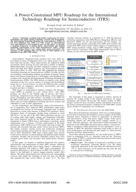
A Power-Constrained <strong>MPU</strong> Roadmap <strong>for</strong> <strong>the</strong> <strong>International</strong><strong>Technology</strong> Roadmap <strong>for</strong> Semiconductors (ITRS)Kwangok Jeong ‡ and Andrew B. Kahng †‡† CSE and ‡ ECE Departments, UC San Diego, La Jolla, CAkjeong@vlsicad.ucsd.edu, abk@cs.ucsd.eduAbstract— <strong>Technology</strong> <strong>roadmap</strong>s help predict requirements <strong>for</strong> futuretechnologies and guide ongoing technology research and development.The <strong>International</strong> <strong>Technology</strong> Roadmap <strong>for</strong> Semiconductors (ITRS) [1]has been published since 1999; it is fully revised in odd-numberedyears and updated in even-numbered years. In this paper, we describea modeling framework to predict future characteristics and impliedtechnology requirements of <strong>the</strong> ITRS microprocessor (<strong>MPU</strong>) ‘systemdriver’, following Moore’s Law scaling under <strong>power</strong> constraints. Theoutcomes of this modeling ef<strong>for</strong>t are <strong>the</strong> basis of ITRS updates to bepublished in <strong>the</strong> 2009 ITRS edition.I. INTRODUCTIONSemiconductor integrated-circuit products have seen rapid improvementsin terms of integration level, cost, speed, <strong>power</strong>, etc. <strong>for</strong>more than four decades. These improvements are enabled by R&Dinvestments whose growing size has motivated a number of industryR&D partnerships, consortia, and o<strong>the</strong>r cooperative ventures. To helpguide and align <strong>the</strong>se R&D programs, <strong>the</strong> Semiconductor IndustryAssociation (SIA) in 1992, 1994 and 1997 published <strong>the</strong> National<strong>Technology</strong> Roadmap <strong>for</strong> Semiconductors (NTRS). In 1998, <strong>the</strong> SIAwas joined by corresponding industry associations in Europe, Japan,Korea, and Taiwan to participate in a 1998 update of <strong>the</strong> Roadmap andto begin work toward <strong>the</strong> first <strong>International</strong> <strong>Technology</strong> Roadmap <strong>for</strong>Semiconductors (ITRS). The ITRS delivers an industry-wide, globalconsensus on <strong>the</strong> best current estimate of research and developmentneeds out to a 15-year horizon. As such, <strong>the</strong> ITRS provides a guideto <strong>the</strong> ef<strong>for</strong>ts of companies, universities, governments, and o<strong>the</strong>rresearch providers or funders.With respect to semiconductor industry evolution, <strong>the</strong> microprocessor(<strong>MPU</strong>) is regarded as a key ‘system driver’, since <strong>MPU</strong>products are often at <strong>the</strong> leading edge of process and devicetechnology, integration level, design methodology, clock frequency,<strong>power</strong> consumption and o<strong>the</strong>r metrics. According to <strong>the</strong> ITRS [1],<strong>the</strong> <strong>MPU</strong> model reflects general-purpose instruction-set architectures(ISAs) that are found standalone in desktop and server systems, andembedded as cores in SOC applications.As new technologies and architectures, along with increased levelsof integration, have improved <strong>MPU</strong> per<strong>for</strong>mance, high <strong>power</strong>consumption has become an increasingly important topic of publicdiscussion in recent years because of global CO2 emissions. Powerdissipation limits of packaging (despite being estimated to reach200 W/cm 2 by <strong>the</strong> end of <strong>the</strong> 2007 ITRS timeframe) and <strong>the</strong> costof cooling make high supply voltages and frequencies infeasible.Past clock frequency trends <strong>for</strong> <strong>the</strong> <strong>MPU</strong> system driver have beeninterpreted as future CMOS device per<strong>for</strong>mance (switching speed)requirements (e.g., a historic 17%/year improvement in <strong>the</strong> highper<strong>for</strong>mancebulk CMOS device CV/I metric) that lead to large offcurrentsand extremely thin gate oxides. Given such devices, <strong>MPU</strong>sthat simply continue existing circuit and architecture techniqueswould exceed package <strong>power</strong> limits by factors of nearly 4× by <strong>the</strong>end of 2020; alternatively, <strong>MPU</strong> logic content and/or logic activitywould need to decrease to match package and plat<strong>for</strong>m <strong>power</strong> budgetconstraints. Portable and low-<strong>power</strong> embedded contexts have morestringent <strong>power</strong> limits, and encounter such market-driven obstaclesearlier.In this paper, we propose a modeling framework that capturescharacteristics and requirements of future <strong>MPU</strong> designs, followingMoore’s Law scaling under <strong>power</strong> limits. Figure 1 summarizes ourmodeling approach with respect to <strong>MPU</strong> <strong>power</strong> consumption. Allgeometry in<strong>for</strong>mation is derived based on <strong>MPU</strong> M1 half-pitch (F ),which is <strong>the</strong> half-pitch of typical stagger-contacted metal1 (M1)bitlines. We define representative unit cell layouts and correspondingA-factors that enable <strong>the</strong> modeling of unit cell areas <strong>for</strong> SRAMand standard-cell logic circuit fabrics, in terms of F . We <strong>the</strong>ncalculate transistor density as a function of F . With <strong>the</strong> physicaltechnology parameters from ITRS Process Integration, Devices andStructures (PIDS) [3] [4] and Interconnect [5] [6] chapters, wemodel capacitance density, and finally derive <strong>MPU</strong> <strong>power</strong> model. Ourclosed-<strong>for</strong>m <strong>MPU</strong> <strong>power</strong> model enables analysis of requirements <strong>for</strong><strong>MPU</strong> design parameter scaling, such as <strong>MPU</strong> frequency scaling, inlight of <strong>power</strong> constraints. O<strong>the</strong>r ITRS requirements such as defectdensity are also derived from <strong>the</strong> <strong>MPU</strong> model.Unit Cell LayoutUnit logic cell width (W logic )Unit logic cell height (H logic )Unit SRAM bitcell width (W SRAM )Unit SRAM bitcell height (H SRAM )#Components#Tr. per logic cell (N tr,nand2 )#Tr. per SRAM bitcell (N tr,bitcell )#Logic gates per core (N gates )#Bitcells per core (N bits )#Cores per die (N core )<strong>Technology</strong> (PIDS)Gate length (L g )Gate width (W g )Gate capacitance (C g )Unit-width leakage (I off )Low Power Tech.Switching ratio ()Low-Vth cell ratio ()Fig. 1.M1 Half-Pitch(F)A-Factor(A logic , A SRAM )Unit-Cell Area(U logic ,U SRAM )Transistor Density(D logic ,D SRAM )Capacitance Density(D cap,logic , D cap,SRAM , D cap,int )Power Density(D dynamic ,D static )<strong>MPU</strong> Power(P)Data flow <strong>for</strong> <strong>MPU</strong> <strong>power</strong> modeling.Metal1 (M1) PitchM1 half-pitch (F)= M1 pitch / 2Design RulesMetal2 routing pitch (p M2 )Poly-to-poly pitch (p poly )Design OverheadLogic layout overhead (O logic )SRAM layout overhead (O SRAM )<strong>Technology</strong> (Interconnect)Interconnect capacitance (C int )Interconnect density (D l,max )Operating ConditionVoltage (V)Frequency (f)The remainder of this paper is organized as follows. Section IIpresents <strong>the</strong> scaling trends of <strong>the</strong> required parameters <strong>for</strong> <strong>power</strong>estimation, and Section III presents <strong>the</strong> density models of <strong>MPU</strong>designs. Section IV gives our <strong>power</strong> models, and Section V discusses<strong>the</strong> <strong>power</strong>-<strong>constrained</strong> frequency <strong>roadmap</strong> <strong>for</strong> <strong>the</strong> ITRS <strong>MPU</strong> systemdriver. Section VI summarizes our conclusions.II. TECHNOLOGY SCALING FOR THE 2009 ITRSBasic physical technology parameters which serve as input parameters<strong>for</strong> <strong>power</strong> estimation are modeled in various chapters of <strong>the</strong> ITRS.Dynamic <strong>power</strong> estimation is based on capacitance of transistorsand interconnects, along with <strong>power</strong> supply voltage. Static <strong>power</strong>estimation requires per unit-width device leakage current (I off )values. Relevant transistor- and interconnect-related parameters arepredicted in <strong>the</strong> ITRS PIDS and Interconnect chapters, respectively. 1Table I summarizes ITRS predictions <strong>for</strong> key parameters, versus atimeline of <strong>MPU</strong> M1 half-pitch (minimum metal width or space ofgiven technologies) and <strong>the</strong> physical gate length (L) which governstransistor electrical characteristics.Given <strong>the</strong>se physical parameters, we can model <strong>power</strong> of <strong>MPU</strong>sbased on integration level, i.e., transistor count per die. Transistorcount scaling of <strong>MPU</strong>s is determined following historical and current<strong>MPU</strong> design trends as follows.• Moore’s Law. The number of transistors is doubled at everytechnology generations, following Moore’s Law. We definetechnology √ generation at <strong>the</strong> time when M1 half-pitch becomes2;2× more transistors can be packed into <strong>the</strong> same die areaas with previous technology.1 Transistor-related parameters are obtained by ITRS contributors using <strong>the</strong>Model <strong>for</strong> Assessment of CMOS Technologies And Roadmaps (MASTAR)[2].978-1-4244-5035-0/09/$26.00 ©2009 IEEE -49- ISOCC 2009
TABLE ITECHNOLOGY PARAMETER SCALING IN ITRS.† : Preliminary values <strong>for</strong> ITRS 2009. Transistor types: HP = high-per<strong>for</strong>mance; LOP = low operating <strong>power</strong>; LSTP = low standby <strong>power</strong>.‡ : Values from ITRS 2008 updates [6], being updated <strong>for</strong> ITRS 2009.†‡ Values from ITRS 2008 updates [4]. Anticipated ITRS 2009 Ioff values of HP and LSTP transistors are 0.1μA and 0.1nA, respectively.<strong>Technology</strong> year 2009 2010 2011 2012 2013 2014 2015 2016 2017 2018 2019 2020 2021 2022 2023 2024Dimensions<strong>MPU</strong> Half-Pitch (nm) † 54 45 38 32 27 24 21 18.9 16.9 15.0 13.4 11.9 10.6 9.5 8.4 7.5Physical Lgate (HP) (nm) † 29 27 24 22 20 18 17 15 14.0 12.8 11.7 10.7 9.7 8.9 8.1 7.4Supply Voltage ParametersVDD (HP) † 1.00 0.97 0.93 0.90 0.87 0.84 0.81 0.78 0.76 0.73 0.71 0.68 0.66 0.64 0.62 0.60VDD (LOP) † 0.95 0.95 0.85 0.85 0.80 0.80 0.75 0.75 0.70 0.70 0.65 0.65 0.60 0.60 0.60 0.60Interconnect-Related ParametersCapacitance (pF/cm) ‡ 1.75 1.75 1.75 1.65 1.65 1.65 1.55 1.55 1.55 1.40 1.40 1.40 1.20 1.20 - -Total length (Km/cm 2 ) ‡ 2.00 2.22 2.50 2.86 3.13 3.57 4.00 4.55 5.00 5.56 6.25 7.14 7.69 9.09 - -Transistor-Related ParametersIoff (HP) (μA/um) †‡ 0.17 0.46 0.71 0.70 0.64 0.69 0.57 0.62 0.56 0.55 0.38 0.40 0.44 0.48 - -Ioff (LSTP) (pA/um) †‡ 30.5 30.7 30.2 30.2 30.9 31.7 30.2 31.0 32.7 33.8 26.2 23.9 33.8 28.9 - -Cg,total (HP) (fF/μm) † 1.00 0.98 0.93 0.96 0.97 0.75 0.76 0.71 0.67 0.64 0.58 0.55 0.53 0.50 0.48 0.46• Constant die area. Die area is assumed to be constant over<strong>the</strong> course of <strong>the</strong> <strong>roadmap</strong>, and is broken into logic, memory(SRAM), and integration overhead components. For given diearea, <strong>the</strong> number of logic and memory transistors are decided,consistent with integration overhead area <strong>for</strong> analog and mixedsignalcores, I/O blocks, whitespace between blocks, etc., whichis assumed to be around 30% of die area.• Multi-core organization. Multiple processing units in <strong>the</strong> <strong>MPU</strong>product chip was modeled starting with <strong>the</strong> 2001 ITRS and <strong>the</strong>130nm technology node. The <strong>MPU</strong> model assumes a multi-coreorganization with shared memory.Initial numbers of cores, logic transistors per core, and SRAMcache size (bytes) per die in 2007 were assumed to be 4, 50Mtx, 2and 16MBytes, respectively; this content fits in 310mm 2 die areawith reasonable integration overhead.The ITRS <strong>MPU</strong> model grows number of transistors at <strong>the</strong> samepace as M1 half-pitch scaling. From year 2009 to 2013, M1 half-pitchshrinks by 2× every two years, and from year 2014 to 2022 by 2×in every 3.5 years. Based on multi-core design trends, we scale <strong>the</strong>number of cores and <strong>the</strong> number of transistors per core by √ 2× atevery generation, respectively, so that <strong>the</strong> total number of transistorsin a die is doubled at every generation. Table II shows <strong>the</strong> numberof cores and transistors per die from 2009 to 2024. 3III. DENSITY MODEL<strong>MPU</strong> design-specific parameter scaling was presented in SectionII. In this section, we discuss <strong>the</strong> detailed modeling approaches <strong>for</strong>design-specific parameters, such as design area and density, in termsof M1 half-pitch. We model <strong>the</strong> area of logic and SRAM separately,<strong>the</strong>n obtain <strong>the</strong> entire <strong>MPU</strong> die area with an integration overheadfactor. From <strong>the</strong> given number of cores in <strong>MPU</strong> and <strong>the</strong> number oftransistors per core, we calculate <strong>the</strong> area and density of transistorsin <strong>MPU</strong>. To model <strong>the</strong> area, we first propose unit layouts of a logiccell and an SRAM bitcell. Then, total area can be calculated bymultiplying <strong>the</strong> area of unit cells and <strong>the</strong>ir respective counts.A. Logic Density ModelUnit logic cell. To determine <strong>the</strong> unit cell size <strong>for</strong> logic, we assumea layout of a unit logic cell, i.e., two-input NAND gate (NAND2),as shown in Figure 2.We only consider simplest design rules. The height and width of<strong>the</strong> unit logic cell are defined by unit drawing pitches. Traditionally,drawing pitch <strong>for</strong> standard cells has been decided from M2 (intermediate)minimum routing pitch values. However, as <strong>the</strong> restricteddesign rule (RDR) is introduced, poly pitch can be used as <strong>the</strong> unitpitch <strong>for</strong> width direction, and M1 (or M2) minimum routing pitchcan be used as <strong>the</strong> unit pitch <strong>for</strong> height direction.For width calculation, we consider two types of NAND2 implementation.Figure 2(a) shows a traditional NAND2 gate drawn by M22 Mtx (Btx) stands <strong>for</strong> million (billion) transistors.3 For SRAM transistor count, we assume six transistors per bitcell, and ninebitcells per byte including an error correction bit.NWellActivePolyContactM1V1M2Fig. 2. Unit logic cell layout, two-input NAND gate. (a) Traditional layout(b) Regular-poly layout.minimum routing pitch; Figure 2(b) shows <strong>the</strong> regular layout style<strong>for</strong> <strong>the</strong> NAND2 gate. With traditional layout style, NAND2 requiresat least three M2 routing pitches in <strong>the</strong> width direction to connectinput/output pins (A, B, Y) using M2, so <strong>the</strong> NAND2 cell can bedrawn with three M2 pitches in width. With restricted one-directionrouting <strong>for</strong> poly, around four M2 routing pitches are required todraw all intra-cell connections, e.g., source/drain connections. Layersunder M2 do not need to be drawn on routing grid. With adoption ofdesign <strong>for</strong> manufacturability (DFM) techniques, e.g, assist features,poly pitch would be proper to define width ra<strong>the</strong>r than M2 routingpitch. Since <strong>the</strong>re exist two input poly lines and two assist-features at<strong>the</strong> boundaries in a NAND2 gate, four poly lines (three poly pitches)are required. Each product team or company can have different layoutstyles. Considering that we will see more restricted layout styles infuture nodes, we use layout style (b) <strong>for</strong> <strong>the</strong> unit logic cell. Theheight of <strong>the</strong> unit cell can differ based on <strong>the</strong> application domain(high density, high speed, etc.). We assume eight M2 routing tracks<strong>for</strong> <strong>the</strong> cell height.A-factor <strong>for</strong> logic. Let poly-to-poly pitch and M1 and M2 routingpitches be p poly , p M1, and p M2, respectively. Width of <strong>the</strong> logicunit cell can be generalized as “(number of N (or P) transistors+ 1) × p poly ”. Here, p poly is calculated by <strong>the</strong> summation of aminimum poly width, minimum contact width and two times polyto-contactminimum space values. Each parameter value is obtainedby averaging <strong>the</strong> design rules from leading-edge industry designmanuals, and we find that p poly and p M2 can be approximated asa multiple of p M1 or F .p poly ≈ 1.50p M1 =3F (1)p M2 ≈ 1.25p M1 =2.5F (2)Using <strong>the</strong> drawing pitch definitions and <strong>the</strong> number of drawingpitches required <strong>for</strong> <strong>the</strong> layout in Figure 2(b), we can calculate <strong>the</strong>area of <strong>the</strong> unit NAND2 (U nand2 )asU logic = 3p poly × 8p M2 = 45(p M1) 2= 180F 2 = A logic F 2 (3)We now have unit logic cell area in terms of M1 half-pitch (F ) and aconstant (A logic ) which is analogue to <strong>the</strong> A-factor in DRAM bitcell-50- ISOCC 2009
TABLE II<strong>MPU</strong> DESIGN PARAMETER SCALING IN ITRS.<strong>Technology</strong> year 2009 2010 2011 2012 2013 2014 2015 2016 2017 2018 2019 2020 2021 2022 2023 2024#Logic cores per <strong>MPU</strong> 5.66 6.73 8.00 9.51 11.3 12.7 14.3 16.0 18.0 20.2 22.6 25.4 28.5 32.0 36.0 40.0#Tr. per logic core (Mtx) 70.7 84.1 100 119 141 159 178 200 224 252 283 317 356 400 448 504#Logic tr. per <strong>MPU</strong> (Btr.) 0.40 0.57 0.80 1.13 1.60 2.02 2.54 3.20 4.03 5.08 6.40 8.06 10.2 12.8 16.1 20.3#SRAM tr. per <strong>MPU</strong> (Btr.) 1.81 2.56 3.62 5.12 7.25 9.13 11.5 14.5 18.3 23.0 29.0 36.5 46.0 58.0 73.0 92.0area estimation which has been used in ITRS. 4Area and density model <strong>for</strong> logic. From <strong>the</strong> unit cell area and gatecount <strong>for</strong> <strong>the</strong> die, we can calculate <strong>the</strong> total area of logic transistors(S logic )asS logic = O logic U logic N coreN gate (4)where N core and N gate are <strong>the</strong> number of cores in a die and<strong>the</strong> number of logic gates used in a core, respectively, and O logicrepresents a design area overhead due to design integration, such aswhitespace area <strong>for</strong> placement flexibility and <strong>power</strong> planning area,etc. We use 2.0 <strong>for</strong> O logic in our model.Transistor density of logic area is <strong>the</strong>n calculated by dividing <strong>the</strong>number of transistors by <strong>the</strong> derived logic area area (S logic ).D tr,logic = N tr,logic /S logic = N tr,nand2 /(O logic U logic ) (5)where <strong>the</strong> number transistors in a NAND2 gate (N tr,nand2 ) is four,based on our unit cell definition.B. SRAM Density ModelUnit SRAM bitcell. From <strong>the</strong> conventional 6T SRAM bitcell layout,we use <strong>the</strong> layout in Figure 3 as <strong>the</strong> unit SRAM bitcell.Fig. 3. SRAM 6-T bitcell schematic and layout.In height direction, we can observe that two parallel poly linesmust be placed. There<strong>for</strong>e, height can be modeled as “2p poly ”. Bitcellwidth is determined by three distances; 1) Wordline contact to bitlinecontact, 2) N-active to <strong>the</strong> next N-active, and 3) transistor widths.The distance from <strong>the</strong> wordline contact to bitline contact can bedefined by minimum metal design rules, and <strong>the</strong> distance from N-active to <strong>the</strong> next N-active can be determined by <strong>the</strong> maximum ofdistance calculated from metal design rules or distance calculatedfrom diffusion design rules. In Figure 3, we can observe that fivemetal routing pitches are required in width direction.A-factor <strong>for</strong> SRAM bitcell. Similar with <strong>the</strong> logic A-factor, aftermodeling <strong>the</strong> height and width, <strong>the</strong> unit area <strong>for</strong> an bitcell(U SRAM) can be modeled using A-factor <strong>for</strong> SRAM (A SRAM) andM1 half-pitch (F ).U SRAM = 2p poly × 5p M1 = 15(p M1) 2= 60F 2 = A SRAMF 2 (6)Area and density model <strong>for</strong> SRAM. Using <strong>the</strong> unit cell area,we can calculate <strong>the</strong> total area occupied by SRAM transistors in <strong>the</strong><strong>MPU</strong>:S SRAM = O SRAMU SRAMN coreN bits (7)where N bit is <strong>the</strong> number of bits per core, and O SRAM represent aSRAM design overhead due to peripheral circuits, such as precharging,sensing and input/output muxing and buffering circuits. Fromindustry SRAM layout data, we use 1.6 <strong>for</strong> O SRAM.Transistor density of <strong>the</strong> SRAM layout region area isD tr,SRAM = N tr,bitcell /(O SRAMU SRAM) (8)where <strong>the</strong> number of transistors in a bitcell (N tr,bitcell) is six.4 A-factor <strong>for</strong> logic is calculated as 180 in Eq. (3). However, after fittingwith actual data collected from industry cell libraries, we decide to use 175<strong>for</strong> <strong>the</strong> logic A-factor.IV. <strong>MPU</strong> POWER MODELIn this section, we propose a closed-<strong>for</strong>m <strong>MPU</strong> <strong>power</strong> model using<strong>the</strong> basic parameters in Section II and <strong>the</strong> transistor area and densitymodels in Section III.A. Capacitance Density ModelFor dynamic <strong>power</strong> estimation, we first model <strong>the</strong> capacitancedensity. From Tables PIDS2a and PIDS2b in <strong>the</strong> PIDS chapter, wecan obtain unit width gate capacitance (C g), which includes fringeand overlap capacitances. With <strong>the</strong> average width value (W g) oftransistors, 5 capacitance of a single transistor (C tr) and capacitancedensity areC tr = W gC g (9)D cap,tr = D tr,logicC tr (10)However, not all <strong>the</strong> capacitances consume <strong>power</strong>. We define activecapacitance density considering switching ratio (α), which is <strong>the</strong> ratioof actively charging or discharging nets (devices) to <strong>the</strong> total numberof nets (devices) in design during operation.D cap,active tr = αD cap,tr (11)From Tables INTC2a and INTC2b in <strong>the</strong> Interconnect chapter, wecan obtain <strong>MPU</strong> estimated wirelength density (D l,max ). 6 Consideringrouting congestion and <strong>power</strong> routing regions, we apply an additionalderating factor to interconnect density D l,max and define effectivewirelength D l,eff as 1/3×D l,max . We obtain per-unit length wirecapacitance from <strong>the</strong> ITRS Interconnect Chapter (Tables INTC2aand INTC2b). Since D l,max assumes a stack of one M1 layer andfive intermediate layers, we simply use <strong>the</strong> majority’s characteristicC intermediate . Interconnect capacitance density (D cap,int) and activeinterconnect capacitance density (D cap,active int) are defined asD cap,int = D l,eff C intermediate (12)D cap,active int = αD cap,int (13)Finally, total active capacitance density is calculated asD cap,logic = D cap,active tr + D cap,active int (14)B. Dynamic Power Density ModelFor dynamic <strong>power</strong> estimation, we assume that <strong>MPU</strong> logic consistsof low standby <strong>power</strong> transistors (LSTP) <strong>for</strong> non-timing critical pathsand high per<strong>for</strong>mance transistors (HP) <strong>for</strong> timing critical paths. βdenotes <strong>the</strong> fraction of HP transistors relative to total logic transistorsin an <strong>MPU</strong> design. 7 We also assume that <strong>the</strong> switching activity ofLSTP transistors is 1/3× that of HP transistors. Dynamic <strong>power</strong>density in <strong>the</strong> logic area isD dynamic,logic = D cap,logic fVHP(β 2 + 1 )3 (1 − β) (15)Capacitance density of <strong>the</strong> SRAM region can be calculated similarly,and can be higher than that of logic. However, only a bitlineand a wordline become active during operation. There<strong>for</strong>e, <strong>the</strong>active capacitance density of SRAM blocks can be considered tobe relatively smaller than that of logic. In our work, we simplyassume that <strong>the</strong> dynamic <strong>power</strong> density of SRAM (D dynamic,SRAM )is 1/10× that of logic.5 Average transistor width is assumed to be 5F .6 Total interconnect length in 1cm 2 die is calculated by assuming that onlyone of every three minimum pitch wiring tracks <strong>for</strong> metal1 (M1) and fiveintermediate levels of interconnects are populated. The wiring lengths <strong>for</strong> eachlevel are <strong>the</strong>n summed to calculate <strong>the</strong> total interconnect length per squarecentimeter of active area.7 The portions of HP and LSTP transistors are assumed as 10% and 90%,respectively.-51- ISOCC 2009
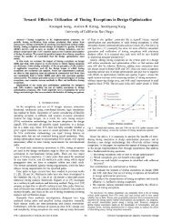
C. Static Power Density ModelWe use <strong>the</strong> same transistor constituent assumption (β) in calculatinglogic static <strong>power</strong> density.D static,logic =0.5D tr,logicV HP× (βI off,HP +(1− β)I off,LST P ) (16)where <strong>the</strong> constant factor 0.5 represents that ei<strong>the</strong>r NMOS or PMOStransistors in a logic cell are off-state at any given time.For SRAM static <strong>power</strong> density, we again assume that multi-Vthtechnique is used, so that bitcell array uses LSTP transistors, andonly β amount of transistors in <strong>the</strong> periphery are HP transistors.D static,SRAM =0.5D tr,SRAM V HP×{ OSRAM − 1 (βI off,HP +(1− β) I off,LST P )O SRAM1+ I off,LST P } (17)O SRAMD. Total <strong>MPU</strong> Power ModelFinally, total <strong>MPU</strong> <strong>power</strong> is given byP total =(D dynamic,logic + D static,logic ) S logic+(D dynamic,SRAM + D static,SRAM ) S SRAM (18)V. POWER-CONSTRAINED <strong>MPU</strong> FREQUENCY MODELBased on <strong>the</strong> area, density and <strong>power</strong> models, o<strong>the</strong>r <strong>MPU</strong> designparameters, e.g., chip size, integration level and operating frequency,must be considered carefully to not exceed a permitted <strong>power</strong> limit. 8To keep up with Moore’s Law, <strong>the</strong> transistor count scaling needsto follow <strong>the</strong> <strong>MPU</strong> design integration trends described in SectionII. We evaluate integration overhead values, which is <strong>the</strong> ratio of<strong>the</strong> remaining area to <strong>the</strong> total die area after subtracting logic andmemory transistors area, using <strong>the</strong> proposed new A-factor modelsand <strong>the</strong> transistor count scaling trends. With <strong>the</strong> old 310mm 2 diearea, <strong>the</strong> integration overhead grows to an unreasonable 41% over <strong>the</strong>course of <strong>the</strong> <strong>roadmap</strong>. To maintain reasonable integration overhead,we reduce die size to 260mm 2 , which matches recently reported<strong>MPU</strong> products 9 and leads to 29.5% of integration overhead.For <strong>MPU</strong> <strong>power</strong> <strong>roadmap</strong> with fixed die size and transistor countscaling, key levers at <strong>the</strong> design stage are frequency and switchingactivity factor. Figure 4 shows <strong>the</strong> dynamic and static <strong>power</strong> predictionsbased on our <strong>power</strong> model, using <strong>the</strong> PIDS device CV/I scalingfactor (13% per year) as a frequency scaling factor. Due to aggressivestandby <strong>power</strong> reduction techniques, such as multi-Vth, multi-Lgate,<strong>power</strong>-gating, etc., and development of low-leakage transistors, static<strong>power</strong> does not increase rapidly. However, dynamic <strong>power</strong> increasesand exceeds 200W in 2015.7006005004003002001000Dynamic Power (W)Static Power (W)2009201020112012201320142015201620172018201920202021202220232024Fig. 4. Dynamic and static <strong>power</strong> prediction <strong>for</strong> <strong>MPU</strong>s. Frequency scalingfactor is 13% per year and switching ration is fixed at 15%.To mitigate this rapid dynamic <strong>power</strong> scaling, we introduces adesign factor which is used to reduce switching activity, into dynamic<strong>power</strong> estimation. Initial switching activity in 2007 is assumed to be0.15, and we introduce a 5% reduction of switching activity per year(α N =0.95α N−1). This implies that low-<strong>power</strong> techniques to reduce<strong>the</strong> switching activity of a design must be developed to continue8 The <strong>power</strong> limit <strong>for</strong> a plat<strong>for</strong>m, e.g., desktop PC, is viewed as having a130-150W limit due to market <strong>for</strong>ces.9 The die size of 45nm CPUs, i.e., Intel R○Core TM i7 (Bloomfield) [7] andAMD Opteron TM (Shanghai) [8] are 263mm 2 and 258mm 2 , respectively.Moore’s Law scaling of <strong>the</strong> <strong>MPU</strong> product class. Using 5% switchingactivity reduction factor, we can reduce dynamic <strong>power</strong> due to <strong>the</strong>active capacitance density as shown in Figure 5.700 Dynamic Power (W)600 Active Capacitance Density (nF/mm^2)50040030020010002009201020112012201320142015201620172018201920202021202220232024(a)700Dynamic Power (W)600 Actiave Capacitance Density (nF/mm^2)50040030020010002009201020112012201320142015201620172018201920202021202220232024Fig. 5. (a) Power prediction with 13% per year CV/I scaling with fixed 0.15switching ratio. (b) Power prediction with 13% per year CV/I scaling with5% switching ratio reduction factor per year from an initial 0.15 switchingratio.However, <strong>power</strong> still increases rapidly, so that <strong>power</strong> exceeds 200Win year 2019. This is mainly due to <strong>the</strong> fast 13% per year device CV/Iscaling. To maintain a reasonable <strong>power</strong> value <strong>for</strong>ced by markets, <strong>the</strong>frequency scaling needs to slow down. At 8% improvement per yearof frequency scaling, <strong>the</strong> maximum <strong>MPU</strong> <strong>power</strong> is 132W throughout<strong>the</strong> <strong>roadmap</strong> years as shown in Figure 6.6050403020100Frequency (GHz) with 13% per year increaseFrequency (GHz) with 8% per year increaseTotal <strong>power</strong> (W) <strong>for</strong> 13% per year frequency scalingTotal <strong>power</strong> (W) <strong>for</strong> 8% per year frequency scaling2009201020112012201320142015201620172018201920202021202220232024Fig. 6. Power-<strong>constrained</strong> frequency scaling. 8% per year scaling offrequency can meet 200W <strong>power</strong> limit.The per<strong>for</strong>mance gap between <strong>the</strong> device and <strong>MPU</strong> can be utilized<strong>for</strong> fur<strong>the</strong>r improvement in design size and <strong>power</strong>, since fasttransistors will allow <strong>for</strong> use of smaller cell sizes during timingoptimization. We note that <strong>the</strong> 8% frequency scaling trajectory needsto be met only by <strong>the</strong> large-sized <strong>MPU</strong> as we assumed. If we donot increase #functions, and shrink and improve current-generationdesigns, when <strong>power</strong> per die is smaller than <strong>the</strong> plat<strong>for</strong>m limit we canuse <strong>the</strong> maximum device scaling factor (13%/year) as <strong>the</strong> frequencyscaling factor.VI. CONCLUSIONSWe describe a consistent, holistic modeling approach <strong>for</strong> <strong>MPU</strong>area, <strong>power</strong> and frequency <strong>roadmap</strong>ping that <strong>for</strong>ms <strong>the</strong> basis <strong>for</strong>planned updates in <strong>the</strong> 2009 edition of <strong>the</strong> ITRS. To maintain Moore’sLaw scaling under <strong>power</strong> constraints, we restrict <strong>MPU</strong> frequencyscaling within <strong>the</strong> envelope of transistor per<strong>for</strong>mance scaling. Inaddition, we highlight <strong>the</strong> looming challenge of improved dynamic<strong>power</strong> reduction, which has recently received less attention than static<strong>power</strong> reduction.REFERENCES[1] <strong>International</strong> <strong>Technology</strong> Roadmap <strong>for</strong> Semiconductors,http://public.itrs.net/.[2] Model <strong>for</strong> Assessment of CMOS <strong>Technology</strong> and Roadmaps(MASTAR), http://www.itrs.net/Links/2007ITRS/LinkedFiles/PIDS/MASTAR5/MASTARDownload.htm.[3] Process Integration, Devices and Structures (PIDS) Chapter in ITRS2007 Edition, http://www.itrs.net/Links/2007ITRS/2007 Chapters/2007 PIDS.pdf.[4] Process Integration, Devices and Structures (PIDS) Chapter in ITRS2008 Updates, http://www.itrs.net/Links/2008ITRS/Home2008.htm.[5] Interconnect Chapter in ITRS 2007 Edition, http://www.itrs.net/Links/2007ITRS/2007 Chapters/2007 Interconnect.pdf.[6] Interconnect Chapter in ITRS 2008 Updates, http://www.itrs.net/Links/2008ITRS/Home2008.htm.[7] Intel R○Core TM i7-920 Processor, Intel, http://ark.intel.com/Product.aspx?id=37147[8] AMD Opteron 2384 Review, http://www.techradar.com/reviews/pcmac/pc-components/processors/amd-opteron-2384-shanghai--484339/specification(b)4003503002502001501005001.210.80.60.40.20-52- ISOCC 2009