TDA7375 - 320Volt
TDA7375 - 320Volt
TDA7375 - 320Volt
- No tags were found...

You also want an ePaper? Increase the reach of your titles
YUMPU automatically turns print PDFs into web optimized ePapers that Google loves.
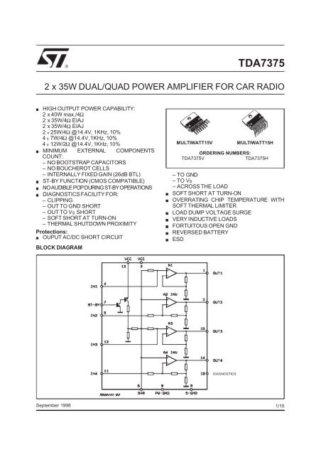
®<strong>TDA7375</strong>2 x 35W DUAL/QUAD POWER AMPLIFIER FOR CAR RADIOHIGH OUTPUT POWER CAPABILITY:2 x 40W max./4Ω2 x 35W/4Ω EIAJ2 x 35W/4Ω EIAJ2 x 25W/4Ω @14.4V, 1KHz, 10%4 x 7W/4Ω @14.4V,1KHz, 10%4 x 12W/2Ω @14.4V, 1KHz, 10%MINIMUM EXTERNAL COMPONENTSCOUNT:– NO BOOTSTRAP CAPACITORS– NO BOUCHEROT CELLS– INTERNALLY FIXED GAIN (26dB BTL)ST-BY FUNCTION (CMOS COMPATIBLE)NOAUDIBLE POPDURING ST-BYOPERATIONSDIAGNOSTICS FACILITY FOR:– CLIPPING– OUT TO GND SHORT– OUT TO VS SHORT– SOFT SHORT AT TURN-ON– THERMAL SHUTDOWN PROXIMITYProtections:OUPUT AC/DC SHORT CIRCUITBLOCK DIAGRAMMULTIWATT15VMULTIWATT15HORDERING NUMBERS:<strong>TDA7375</strong>V<strong>TDA7375</strong>H–TOGND–TOVS– ACROSS THE LOADSOFT SHORT AT TURN-ONOVERRATING CHIP TEMPERATURE WITHSOFT THERMAL LIMITERLOAD DUMP VOLTAGE SURGEVERY INDUCTIVE LOADSFORTUITOUS OPEN GNDREVERSED BATTERYESDDIAGNOSTICSSeptember 19981/15
<strong>TDA7375</strong>ELECTRICAL CHARACTERISTICS (Refer to the test circuit, VS = 14.4V; RL =4Ω; f = 1KHz;Tamb =25°C, unless otherwise specifiedSymbol Parameter Test Condition Min. Typ. Max. UnitV S Supply Voltage Range 8 18 VId Total Quiescent Drain Current RL = ∞ 150 mAV OS Output Offset Voltage 150 mVP O Output Power THD = 10%; R L =4ΩBridgeSingle EndedSingle Ended, R L =2ΩP O max Max. Output Power (***) VS = 14.4V, Bridge 36 40 WP O EIAJ EIAJ Output Power (***) V S = 13.7V, Bridge 32 35 WTHD Distortion R L =4ΩSingle Ended, P O = 0.1 to 4WBridge, P O = 0.1 to 10WCT Cross Talk f = 1KHz Single Endedf = 10KHz Single Endedf = 1KHz Bridgef = 10KHz BridgeR IN Input Impedance Single EndedBridgeGV Voltage Gain Single EndedBridge236.5257120.020.03 0.37060556020 3010 1519 20 2125 26 27G V Voltage Gain Match 0.5 dBE IN Input Noise Voltage R g = 0; ”A” weighted, S.E.Non Inverting ChannelsInverting ChannelsBridgeRg = 0; 22Hz to 22KHz 3.5 µVSVR Supply Voltage Rejection Rg = 0; f = 300Hz 50 dBA SB Stand-by Attenuation P O =1W 80 90 dBI SB ST-BY Current Consumption V ST-BY = 0 to 1.5V 100 µAV SB ST-BY In Threshold Voltage 1.5 VV SB ST-BY Out Threshold Voltage 3.5 VI pin7 ST-BY Pin Current Play Mode V pin7 =5V 50 µAMax Driving Current Under5 mAFault (*)I cd off Clipping Detectord = 1% (**) 90 µAOutput Average CurrentIcd on Clipping Detectord = 5% (**) 160 µAOutput Average CurrentV sat pin10 Voltage Saturation on pin 10 Sink Current at Pin 10 = 1mA 0.7 V(*) See built-in S/C protection description(**) Pin 10 Pulled-up to 5V with 10KΩ; RL=4Ω(***) Saturated square wave output.25WWW%%dBdBdBdBKΩKΩdBdBµVµV3/15
<strong>TDA7375</strong>STANDARD TEST AND APPLICATION CIRCUITFigure 1: Quad StereoST-BY10K R1C710µFC6100nFV SC51000µFIN FLC1 0.22µFIN FR 5IN RLC2 0.22µFC4 0.22µF4 7 13 31C10 2200µFIN RR 11C11 2200µFNote:C3 0.22µFC9, C10, C11, C12 could be146reduced if the 2Ω operation is not8 9 10 C12 2200µFrequired.C8 47µFDIAGNOSTICSD94AU063A12215C9 2200µFOUT FLOUT FROUT RLOUT RRFigure 2: Double BridgeST-BY10K R1C510µFC4100nFV SC31000µFIN L1331C1 0.47µF5OUT LIN RC2 0.47µF1211215OUT RC8 47µF4 7 D94AU064A68 9 1014DIAGNOSTICSFigure 3: Stereo/BridgeST-BY10K10µF100nFVS1000µF4 7 13 3IN L10.22µF2200µFIN L520.22µF2200µFIN BRIDGE 12150.47µF 116148 9 1047µFDIAGNOSTICSD94AU065AOUT LOUT ROUTBRIDGE4/15
<strong>TDA7375</strong>Figure 4: P.C. Board and Component Layout of the fig.1 (1:1 scale).Figure 5: P.C. Board and Component Layout of the fig.2 (1:1 scale).5/15
<strong>TDA7375</strong>High Application FlexibilityThe availability of 4 independent channels makesit possible to accomplish several kinds of applicationsranging from 4 speakers stereo (F/R) to 2speakers bridge solutions.In case of working in single ended conditions thepolarity of the speakers driven by the invertingamplifier must be reversed respect to those drivenby non inverting channels.This is to avoid phase inconveniences causingsound alterations especially during the reproductionof low frequencies.Easy Single Ended to Bridge TransitionThe change from single ended to bridge configurationsis made simply by means of a short circuitacross the inputs, that is no need of further externalcomponents.Gain Internally Fixed to 20dB in Single Ended,26dB in BridgeAdvantages of this design choice are in terms of:components and space savingoutput noise, supply voltage rejection and distortionoptimization.Silent Turn On/Off and Muting/Stand-by FunctionThe stand-by can be easily activated by means ofa CMOS level applied to pin 7 through a RC filter.Under stand-by condition the device is turned offcompletely (supply current = 1µA typ.; output attenuation=80dB min.).Every ON/OFF operation is virtually pop free.Furthemore, at turn-on the device stays in mutingcondition for a time determined by the value assignedto the SVR capacitor.While in muting the device outputs becomes insensitiveto any kinds of signal that may be presentat the input terminals. In other words everytransient coming from previous stages producesno unplesantacoustic effect to the speakers.STAND-BY DRIVING (pin 7)Some precautions have to be taken in the definitionof stand-by driving networks: pin 7 cannot bedirectly driven by a voltage source whose currentcapability is higher than 5mA. In practical casesa series resistance has always to be inserted,having it the double purpose of limiting the currentat pin 7 and to smooth down the stand-byON/OFF transitions - in combination with a capacitor- for output pop prevention.In any case, a capacitor of at least 100nF frompin 7 to S-GND, with no resistance in between, isnecessary to ensure correct turn-on.OUTPUT STAGEThe fully complementary output stage was madepossible by the development of a new component:the ST exclusive power ICV PNP.A novel design based upon the connection shownin fig. 20 has then allowed the full exploitation ofits possibilities.The clear advantagesthis new approach has overclassical output stages are as follows:Rail-to-Rail Output Voltage Swing With NoNeed of Bootstrap Capacitors.The output swing is limited only by the VCEsatof the output transistors, which is in the rangeof 0.3Ω (R sat ) each.Classical solutions adopting composite PNP-NPN for the upper output stage have highersaturation loss on the top side of the waveform.This unbalanced saturation causes a significantpower reduction. The only way to recoverpower consists of the addition of expensivebootstrap capacitors.Absolute Stability Without Any ExternalCompensation.Referring to the circuit of fig. 20 the gainVOut/VIn is greater than unity, approximately 1+R2/R1. The DC output (VCC/2) is fixed by anauxiliary amplifier common to all the channels.By controlling the amount of this local feedbackitis possible to force the loop gain (A*β) tolessthan unity at frequency for which the phase shiftis 180°. This means that the output buffer is intrinsicallystableand not prone to oscillation.Most remarkably, the above feature has beenachieved in spite of the very low closed loopgain of the amplifier.In contrast, with the classical PNP-NPN stage,the solution adopted for reducing the gain athigh frequencies makes use of external RCnetworks, namely the Boucherot cells.BUILT–IN SHORT CIRCUIT PROTECTIONFigure 20: The New Output Stage9/15
<strong>TDA7375</strong>Reliable and safe operation, in presence of allkinds of short circuit involving the outputs is assuredby BUILT-IN protectors. Additionally to theAC/DC short circuit to GND, to VS, across thespeaker, a SOFT SHORT condition is signalledout during the TURN-ON PHASE so assuring correctoperation for the device itself and for theloudspeaker.This particular kind of protection acts in a way toavoid that the device is turned on (by ST-BY)when a resistive path (less than 16 ohms) is presentbetween the output and GND. As the involvedcircuitry is normally disabled when a currenthigher than 5mA is flowing into the ST-BYpin, it is important, in order not to disable it, tohave the external current source driving the ST-BY pin limited to 5mA.This extra function becomes particularly attractivewhen, in the single ended configuration, one capacitoris shared between two outputs (see fig.21).Figure 22: Clipping Detection WaveformsFigure 21.A current sinking at pin 10 is triggered when acertain distortion level is reached at any of theoutputs. This function allows gain compressionpossibility whenever the amplifier is overdriven.Supposing that the output capacitor Cout for anyreason is shorted, the loudspeaker will not bedamaged being this soft short circuit condition revealed.Diagnostics FacilityThe <strong>TDA7375</strong> is equipped with a diagnostic circuitryable to detect the following events:Clipping in the output signalThermal shutdownOutput fault:– short to GND– short to VS– soft short at turn onThe information is available across an opencollector output (pin 10) through a current sinkingwhen the event is detectedThermal ShutdownIn this case the output 10 will signal the proximityof the junction temperature to the shutdownthreshold. Typically current sinking at pin 10 willstart ~10°C before the shutdown threshold isreached.HANDLING OF THE DIAGNOSTICS INFORMA-Figure 23: Output Fault Waveforms (see fig. 24)<strong>TDA7375</strong>10/15
<strong>TDA7375</strong>Figure 24: Fault WaveformsST-BY PINVOLTAGE2VOUT TO Vs SHORTtOUTPUTWAVEFORMSOFT SHORTOUT TO GND SHORTtVpin 10CORRECT TURN-ONFAULT DETECTIONtCHECK AT TURN-ON(TEST PHASE)D94AU149ASHORT TO GNDOR TO VsTIONAs various kinds of information is available at thesame pin (clipping detection, output fault, thermalproximity), this signal must be handled properly inorder to discriminate each event.This could be done by taking into account the differenttiming of the diagnostic output during eachcase.Figure 25: WaveformsST-BY PINVOLTAGEtVsOUTPUTWAVEFORMtVpin 10WAVEFORMD94AU150CLIPPINGSHORT TO GNDOR TO VsTHERMALPROXIMITYt11/15
<strong>TDA7375</strong>Normally the clip detector signalling produces alow level at pin 10 that is shorter than that presentunder faulty conditions; based on this assumptionFigure 26.an interface circuitry to differentiate the informationis represented in the schematic of fig. 26.<strong>TDA7375</strong>PCB-LAYOUT GROUNDING (general rules)The device has 2 distinct ground leads, P-GND(POWER GROUND) and S-GND (SIGNALGROUND) which are practically disconnectedfrom each other at chip level. Proper operation requiresthat P-GND and S-GND leads be connectedtogether on the PCB-layout by means ofreasonablylow-resistance tracks.As for the PCB-ground configuration, a star-likearrangement whose center is represented by thesupply-filtering electrolytic capacitor ground ishighly advisable. In such context, at least 2 separatepaths have to be provided, one for P-GNDand one for S-GND. The correct ground assignmentsare as follows:STANDBY CAPACITOR, pin 7 (or any otherstandby driving networks): on S-GNDSVR CAPACITOR (pin 6): on S-GND and to beplaced as close as possible to the device.INPUT SIGNAL GROUND (from active/passivesignal processor stages): on S-GND.SUPPLY FILTERING CAPACITORS (pins 3,13):on P-GND. The (-) terminal of the electrolytic capacitorhas to be directly tied to the battery (-) lineand this should represent the starting point for allthe ground paths.12/15