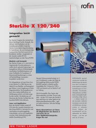
Download - Rofin
Download - Rofin
Download - Rofin

You also want an ePaper? Increase the reach of your titles
YUMPU automatically turns print PDFs into web optimized ePapers that Google loves.
PERFECT MARKS – SHARP CUTS■ SEMICONDUCTOR INDUSTRY ■ LASER ■ ROFINWE THINK LASER
High-precision semiconapplicationsHigh-speed marking ondifferent compoundsHigh-quality isolation cuton TFTL = 36,125 μmLeading Laser Solutions for theSemiconductor IndustryMarking solutions for mobile devicesComprehensive Laser SelectionBacked by many years of experience in laser material processing, ROFINoffers you a comprehensive product line for the semiconductor industry. Ourportfolio ranges from laser sources to turn-key solutions for micro andmarking applications such as LED processing, IC and wafer marking,leadframe marking, TFT cutting and IC decapping. Available laser technologiesreach from efficient fiber lasers, to compact end-pumped and transversallypumped lasers with different wavelengths, to disc lasers. Working closelywith our customers and partners, we have established considerable expertise incustomer-specific solutions.Worldwide Customer ServiceROFIN's first-class laser systems feature the company's own laser technologydesigned for low maintenance, cost-efficient and reliable operation. Whateveryou require, whether beam sources or high-precision all-in-one solutions,you will find it at ROFIN. With worldwide sales and service network andexperienced R&D, ROFIN has optimum, single-source solutions for a varietyof semicon applications.
LED production processesHybrid cutting of QFNWafer ID MarkingLCD PanelDiffusorLED BacklightBest Solutions for Well-Established andUpcoming MarketsPCB markingA Standard in Semiconductor ManufacturingLaser marking and laser material processing are well established in variousapplication fields in the semiconductor industry. In wafer production lasersare used for traceability marking and scribing. High-speed laser marking onmold compounds, metal housings or wafer backsides is an essential finalproduction step for any semiconductor device. Applications besides markinginclude cutting of leadframes and deflashing as well as processing ofcompound materials, such as hybrid cutting of QFN packages and separationof irregular shaped multimedia cards.Indispensable for Efficient Production of LCD PanelsWhether only a few centimeters big or screen sizes of over 50 inches – hardlyany electronic device can do without an LCD display these days. For the efficientproduction of TFT-LCD panels, rows and columns of the matrix are initiallyconnected. In a later production step this connection must be cut with the laser– accurately and absolutely reliably but with high speed as well.Reliable High Speed Marking – LED Processing with LasersLEDs are developing to one of the predominant light sources over the comingdecades. Among the most promising application areas are the LED displaybacklight technology and high-power LEDs in the automotive and mobile phoneindustry. Laser marking is an essential step in manufacturing high-powerLEDs as well as LEDs used for LCD panel backlighting. ROFIN's strengths arethe real-time compensation of position tolerances which is indispensable fora reliable production process.
End-pumpedLaser Beam SourceFiber Laser MarkerDisc LaserField-Tested Technology,Ready for 24/7 ProductionLaser marker / double head configurationTried and Tested Laser Sources for Any Type of ApplicationAll ROFIN lasers feature compact design, low operational cost, high availabilitywith low maintenance and easy integration with virtually any handlingconfiguration. They use state-of-the-art laser technology, comprising diodeend-pumped and side-pumped rod lasers as well as fiber and disc lasersand are available with different output powers. Depending on laser power,the systems are completely air-cooled or use air-to-water cooling. Withwavelengths of 1064 nm, 532 nm and 355 nm, virtually any material usedin semiconductor manufacturing such as mold compounds, silicon, epoxy,ceramics, etc. can be processed efficiently.Comprehensive Application KnowledgeROFIN offers a comprehensively equipped laser application lab. Customerapplications and lab studies can be carried out with the assistance ofexperienced engineers. Practically all of ROFIN's marking systems areavailable for application trials. Based on characteristic application data, thematerial to be processed, the desired marking geometry and constraints ofthe process environment, ROFIN presents all possible laser concepts forconsideration, with benefits and implications.
IC markingLED markingTraceabilitymarking of wafersMarking ApplicationsWaferlase ID 200IC MarkingROFIN's laser markers generate characters at sizes precisely in accordancewith the user's requirements. They still ensure best quality even at very smallcharacter sizes. Line widths are selectable with controlled material penetrationdepths. Integrated circuit packages – mold compound, epoxy or ceramics –can be processed with reliable and predictable results. For marking directly onsilicon or PCB, the use of 532 nm lasers is essential. These dedicated solutionsarchive high contrast with excellent performance at small character heights.LED MarkingNot only the automotive industry asks for complete traceability of everysingle high-power LED today. Fequency-doubled PowerLine lasers markleadframes during the LED production process with minuscule 2D matrixcodes. They also mark white ceramics used as substrate for LEDs, with verysmall character heights and line widths.Traceability Marking of WafersOur Waferlase systems produce traceability markings on transparent, semitransparentand opaque wafer materials used for IC and high-power LEDproduction. Two methods are used which differ in terms of process, depthand location of the mark. With the "hard" marking method, which producesdurable marking even after a large number of etching and polishing steps,the dots have a depth of up to 90 micrometers and are created throughmaterial ablation. Debris-free marking, which is set for clean-roomenvironments, is just 2.5 µm deep, and is achieved solely by melting ofthe silicon.
Package decappingLaser deflashingEnd-pumped laser markerCutting ApplicationsTFT CuttingThe columns and rows of a TFT pixel matrix are activated using transparentindium tin oxide (ITO) conductive paths. For efficient production of TFT displays,a conductive connection must be established between the columns and rowsof the matrix. In a later production step, the lasers will cut the ITO conductivepaths with a fine line and at high speed.Cutting of μSD cardsSeparation of QFN PackagesSeparation of QFN packages is a challenge in the production process so fardue to the need to cut a combination of soft and hard material. A newhybrid cutting technology, using the disc laser StarDisc and mechanicalsawing, increases the production output significantly. The process is twice asfast and saw blade lifetime is quintupled.Cutting of Multimedia CardsLaser technology used for isolating of MMC cards is in particular beneficialin its environmental and cost aspects. Water jet cutting, commonly used forcutting compound plastic materials, requires substantial ecological efforts ofpurifiying cutting water which is polluted with abrasive particles.DeflashingExcess encapsulation material on unmolded surfaces can have seriousnegative impact on proper contacting or optimum thermal conduction. Laserdeflashing systems use integrated pattern recognition to identify crucialareas and remove excess mold with a diode pumped solid state laser.DecappingDecapping is a precisely-controlled laser process which ablates layers of themolding compound and reveals the inner structures for failure analysis.Compared to chemical cauterizing or other procedures, the laser allowsselective ablation of certain areas and removing of the compoundunderneath the wiring.
Specially designedSemicon objects softwareSemicon SoftwareFunctionsIntegration in FactoryControl SystemsPowerful and Simple to Use SoftwareEasy OperationEach laser marker comes with a powerful, entirely customizable softwarepackage based on Windows XP. Text, logos or graphics can be created withdrag-and-drop functions or imported from existing files. VisualLaserMarker(VLM) is a sophisticated "what you see is what you get" type software andoffers the flexibility to be simple to use and yet powerful. VLM handles a widevariety of marking content e.g. matrix-codes, barcodes and serial numbers.Extremely small marks can be realized depending on the material. The softwarecontrols marking on flat and curved surfaces and even marking-on-the-flyapplications. A built-in wizard provides a variety of templates and assists insetting up marking layout quickly. A preview function helps to check programmingat a glance.Easy IntegrationVLM is able to fully integrate into any production software and is configuredto handle all common communication protocols from (TCP/IP) to SEMI standards(SECS/GEM). VisualLaserMarker functions can be controlled through ActiveXtechnology giving the user full control of the entire laser process.Semicon Key Features■■■■■■■■Matrix Object (for easy setup of Tray and Strip models)JEDEC Tray and Leadframe databaseDevice ID and BinCode Mapping2D codes like datamatrix, QR code and various barcodesSECS-GEM /Remote ControlXML Layout Import / Recipe Up & <strong>Download</strong>Autoteach Interface for Vision InspectionStatus /Data Logging and Unit-Level-Tracking
LASER MICROROFIN-BAASEL LasertechMedical DeviceTechnologyFlexible PackagingSemiconductorJewelrySolar PowerGmbH & Co. KGPetersbrunner Str. 1b82319 StarnbergPhone +49(0)8151-776-0Fax: +49(0)8151-776-4159Email: sales@baasel.deLASER MACROROFIN-SINAR Laser GmbHBerzeliusstraße 8722113 HamburgPhone:+49(0)40-733 63-0Fax: +49(0)40-733 63-4100Email: info@rofin-ham.deSOLUTIONS FROM A SINGLE SOURCE■ WWW.ROFIN.COMLASER MARKINGROFIN-SINAR Laser GmbHDieselstraße 1585232 Bergkirchen/GündingPhone:+49(0)8131-704-0Fax: +49(0)8131-704-4100Email: info@rofin-muc.deAustria: Phone: +49-(0)8151-776-0E-mail: sales@baasel.deBenelux: Phone: +31-(0)78-69310-37E-mail: info@rofin-baasel.nlCanada: Phone: +1-905-607-0400E-mail: info-canada@rofin-inc.comChina: Phone: +86-(0)21-68552216E-mail: info@rofin-baasel.com.cnFrance: Phone: +33-(0)-1-6911-3636E-mail: info@rofin.frGreat Britain:Phone: +44-(0)-1327-701-100E-mail: info@rofin-baasel.co.ukItaly: Phone: +39-039-2729-1E-mail: info@rofin.itJapan: Phone: +81-(0)46-229-8655E-mail: info@rofin-baasel.co.jpSingapore: Phone: +65-6482-1091E-mail: reception@rofin-baasel.com.sgSouth Korea:Phone: +82-(0)2837-1750E-mail: info@rofin-baasel.co.krSpain: Phone: +34-948-324-600E-mail: info@rofin-es.comSwitzerland:Phone: +41-(0)32--3221010E-mail: info@rofin-baasel.ch© ROFIN-SINAR/SEMICON/09.10/E/0.5/V2.0/ROBI-ORTMANN/LUXARTSILK200WE THINK LASERTaiwan:Phone: +886-(0)2-2790-1300E-mail: info@rofin-baasel.com.twUSA: Phone: +1-978 635 91 00E-mail: info@rofin-baasel.com