You also want an ePaper? Increase the reach of your titles
YUMPU automatically turns print PDFs into web optimized ePapers that Google loves.
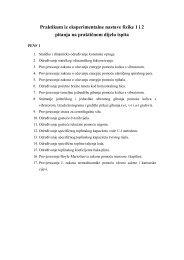
28.13 Energy Bands in Solids 927EnergyConduction electronselectronsholesConduction bandFigure 28.26 Movement ofcharges (holes and electrons) in asemiconductor. The electrons movein the direction opposite the directionof the external electric field, andthe holes move in the direction of thefield.Narrow forbidden gapValence bandApplied E fieldfigure, provide a few empty states called holes for valence band electrons to fill; sosome electrons in the valence band can gain energy and move towards a positiveelectrode and thus also carry the current. Since the valence band electrons that fillholes leave behind other holes, it is equally valid and more common to view theconduction process in the valence band as a flow of positive holes towards the negativeelectrode applied to a semiconductor. Thus, a pure semiconductor, such assilicon, can be viewed in a symmetric way: silicon has equal numbers of mobileelectrons in the conduction band and holes in the valence band. Furthermore,when an external voltage is applied to the semiconductor, electrons move towardthe positive electrode and holes move toward the negative electrode. In the nextsection we will look at the concepts of an electron and a hole in a simpler, moregraphic way as the presence or absence of an outer-shell electron at a particularlocation in a crystal lattice.When small amounts of impurities are added to a semiconductor such assilicon (about one impurity atom per 10 7 silicon atoms), both the band structureof the semiconductor and its resistivity are modified. The process of addingimpurities, called doping, is important in making devices having well-definedregions of different resistivity. For example, when an atom containing fiveouter-shell electrons, such as arsenic, is added to a semiconductor such as silicon,four of the arsenic electrons form shared bonds with atoms of the semiconductorand one is left over. This extra electron is nearly free of its parent atomand has an energy level that lies in the energy gap, just below the conductionband. Such a pentavalent atom in effect donates an electron to the structureand hence is referred to as a donor atom. Because the spacing between the energylevel of the electron of the donor atom and the bottom of the conductionband is very small (typically, about 0.05 eV), only a small amount of thermalenergy is needed to cause this electron to move into the conduction band.(Recall that the average thermal energy of an electron at room temperature is3k B T/2 0.04 eV). Semiconductors doped with donor atoms are called n-typesemiconductors, because the charge carriers are electrons, the charge of whichis negative.If a semiconductor is doped with atoms containing three outer-shell electrons,such as aluminum, the three electrons form shared bonds with neighboring semiconductoratoms, leaving an electron deficiency—a hole—where the fourth bondwould be if an impurity-atom electron was available to form it. The energy level ofthis hole lies in the energy gap, just above the valence band. An electron from thevalence band has enough energy at room temperature to fill that impurity level,leaving behind a hole in the valence band. Because a trivalent atom, in effect, acceptsan electron from the valence band, such impurities are referred to as acceptoratoms. A semiconductor doped with acceptor impurities is known as a p-typesemiconductor, because the majority of charge carriers are positively chargedholes.